

ST TL062, TL062A, TL062BERS User Manual
查询TL062供应商
LOW POWER J-FET DUALOPERATIONAL AMPLIFIERS
■
VERYLOW POWERCONSUMPTION : 200µA
■
WIDE COMMON-MODE (UP TO V
DIFFERENTIALVOLTAGERANGES
■
LOW INPUTBIAS AND OFFSETCURRENTS
■
OUTPUTSHORT-CIRCUIT PROTECTION
■
HIGH INPUT IMPEDANCE J-FET INPUT
STAGE
■
INTERNAL FREQUENCYCOMPENSATION
■
LATCHUP FREE OPERATION
■
HIGH SLEWRATE: 3.5V/µs
CC
+
) AND
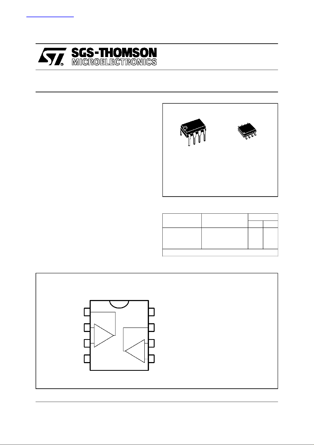
TL062A - TL062B
N
DIP8
(Plastic Package)
TL062
D
SO8
(Plastic Micropackage)
DESCRIPTION
The TL062, TL062A and TL062B are high speed
J-FETinput dualoperationalamplifier family. Each
of these J-FET input operational amplifiers incorporates well matched, high voltage J-FET and bipolar transistors in a monolithicintegratedcircuit.
The devicesfeature highslew rates, lowinput bias
and offsetcurrents,andlowoffsetvoltagetemperature coefficient.
PIN CONNECTIONS (top view)
1
2
3
45
-
+
-
+
ORDER CODES
Part Number Temperature Range
o
TL062M/AM/BM -55
TL062I/AI/BI -40oC, +105oC ●●
TL062C/AC/BC 0oC, +70oC ●●
Example : TL062IN
C, +125oC ●●
8
1 - Output 1
7
6
2 - Inverting input 1
3 - Non-inverting input1
-
4-V
CC
5 - Non-inverting input 2
6 - Inverting input 2
7 - Output 2
+
8-V
CC
Package
ND
October 1997
1/10
TL062 - TL062A - TL062B
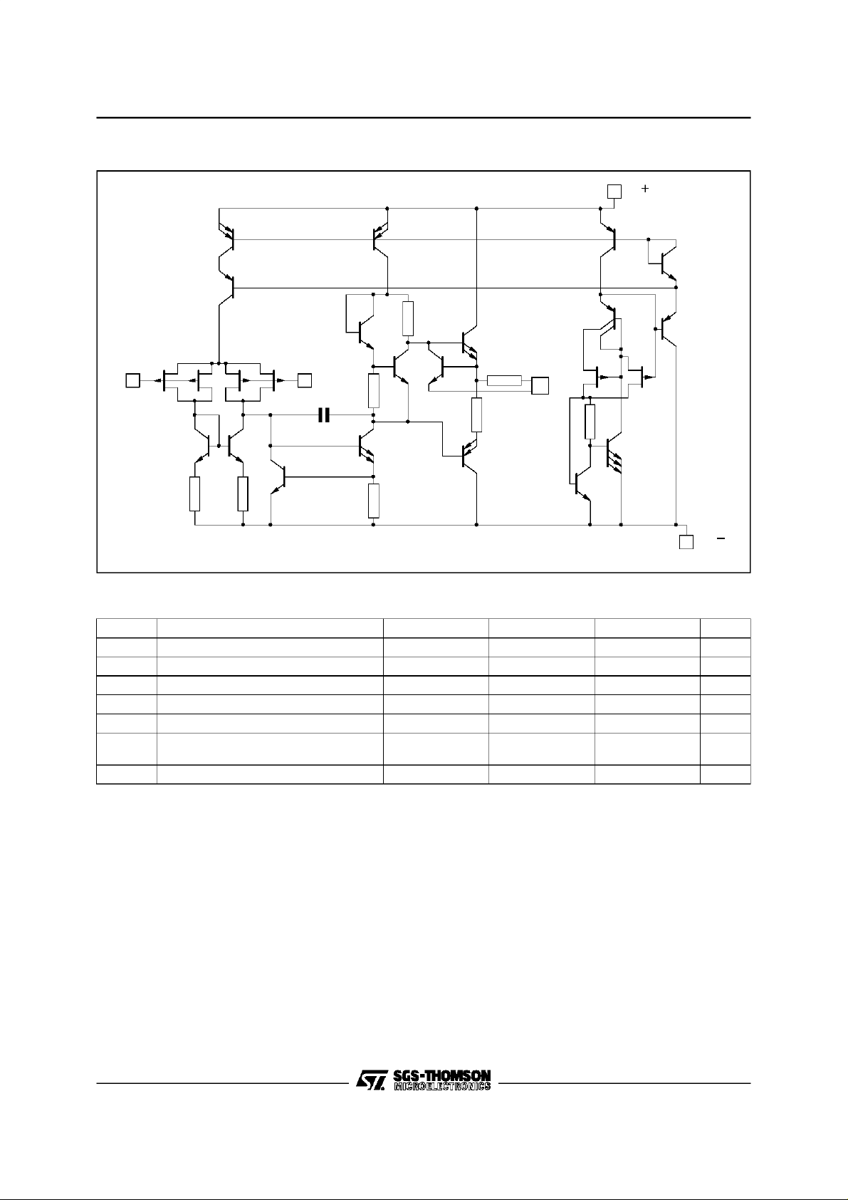
SCHEMATIC DIAGRAM
220
V
CC
Ω
Inverting
Input
4.2k
Ω
Non-inverting
Input
45k Ω
100 Ω
64Ω
270Ω
Output
3.2k
1/2 TL062
Ω
V
CC
MAXIMUMRATINGS
Symbol Parameter TL062M,AM,BM TL062I,AI,BI TL062C,AC,BC Unit
V
V
P
T
T
Notes : 1. All voltage values, except differential voltage, are withrespect to the zero reference level (ground) of the supply voltages where
Supply Voltage - (note1) ±18 ±18 ±18 V
CC
Input Voltage - (note3) ±15 ±15 ±15 V
V
i
Differential Input Voltage- (note 2) ±30 ±30 ±30 V
id
Power Dissipation 680 680 680 mW
tot
Output Short-Circuit Duration (Note 4) Infinite Infinite Infinite
Operating Free-Air Temperature
oper
Range
Storage Temperature Range - 65 to + 150 -65 to + 150 - 65 to + 150
stg
the zero reference level is the midpointbetween V
2. Differentialvoltagesare at the non-inverting input terminal with respect to the inverting input terminal.
3. The magnitude of the input voltage must never exceed the magnitude of the supply voltage or 15 volts, whichever is less.
4. The output may be shorted to ground or to either supply. Temperature and/or supply voltages must be limited to ensure that the
dissipation rating is not exceeded.
-55 to +125 -40 to +105 0 to +70
+
CC
and V
-
.
CC
o
C
o
C
2/10
TL062 - TL062A - TL062B
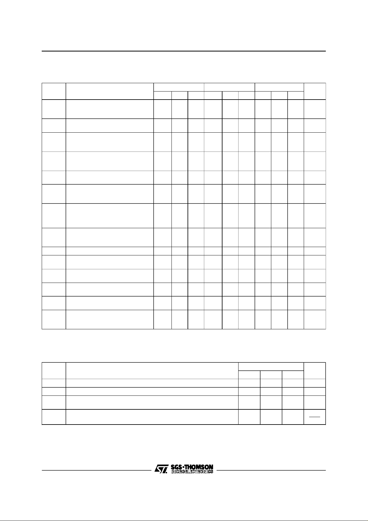
ELECTRICAL CHARACTERISTICS
=± 15V, T
V
CC
Symbol Parameter
V
DV
V
V
A
Input Offset Voltage (Rs=50Ω)
io
Temperature Coefficient of Input
io
Offset Voltage (R
I
Input Offset Current *
io
Input Bias Current *
I
ib
Input Common Mode Voltage
icm
Range
Output Voltage Swing (RL= 10kΩ)
OPP
Large Signal Voltage Gain
vd
(R
L
GBP Gain Bandwidth Product
(T
amb
= 100pF) 1 1 1
C
L
Input Resistance 10
R
i
CMR Common Mode Rejection Ratio
(R
s
SVR Supply Voltage Rejection Ratio
(R
s
I
Supply Current (Per Amplifier)
cc
(T
amb
V
O1/VO2
P
* Input bias currents of a FET-input operational amplifier are normal junction reverse currents, which are temperature sensitive.
Pulse techniques must be used that will maintain the junction temperature as closes to the ambient temperature as possible.
Channel Separation
(A
v
Total Power Consumption
D
(Each Amplifier)
(T
amb
=25oC (unless otherwisespecified)
amb
TL062M TL062I TL062C
Min. Typ. Max. Min. Typ. Max. Min. Typ. Max.
T
T
T
T
T
T
T
T
=25oC
amb
min
amb
min
amb
min.
. ≤ T
. ≤ T
≤ T
amb
max.
=50Ω)101010
s
=25oC
≤ T
amb
max.
=25oC
≤ T
≤ T
max
.
amb
±11.5 +15
=25oC
amb
min
. ≤ T
amb
≤ T
max
.
36
15
5 100
20
30 200
50
±11.5 +15
-12
36
9
5 100
10
30 200
20
-12
30 40010pA
±11 +15
-12
202027 202027 202027
315
5 2005pA
= 10kΩ,Vo=±10V)
T
T
amb
min
=25oC
. ≤ T
amb
≤ T
max
.
4
64
63
4
6
3
4
=25oC, RL= 10kΩ
12
10
12
10
12
= 50Ω) 8086 8086 7076
=50Ω) 8095 8095 7095
=25oC, no load, no signal) 200 250 200 250 200 250
= 100, T
=25oC) 120 120 120
amb
=25oC, no load, no signal) 6 7.5 6 7.5 6 7.5
20
Unit
mV
µV/
nA
nA
V
V
V/mV
MHz
Ω
dB
dB
µA
dB
mW
o
C
ELECTRICAL CHARACTERISTICS (continued)
=± 15V, T
V
CC
Symbol Parameter
SR Slew Rate (V
Rise Time (Vi= 20mV, RL= 10kΩ,CL= 100pF, AV= 1) 0.2 µs
t
r
K
Overshoot Factor (Vi= 20mV, RL= 10kΩ,CL= 100pF, AV=1)
OV
(see figure 1) 10
e
Equivalent Input Noise Voltage
n
(R
s
=25oC
amb
= 10V, RL= 10kΩ,CL= 100pF, AV= 1) 1.5 3.5 V/µs
i
= 100Ω, f = 1KHz) 42
TL062C,I,M
Min. Typ. Max.
Unit
%
nV
√Hz
3/10
 Loading...