

ST TDE1747 User Manual
Interface circuit - relay and lamp-driver
Features
■ Open ground protection
■ High output current
■ Adjustable short-circuit protection to ground
■ Thermal protection with hysteresis to avoid the
intermediate output levels
■ Large supply voltage range: + 8V to +45V
■ Short-circuit protection to V
Description
The TDE1747 is a monolithic comparator
designed for high current and high voltage
applications, specifically to drive lamps, relays,
stepping motors.
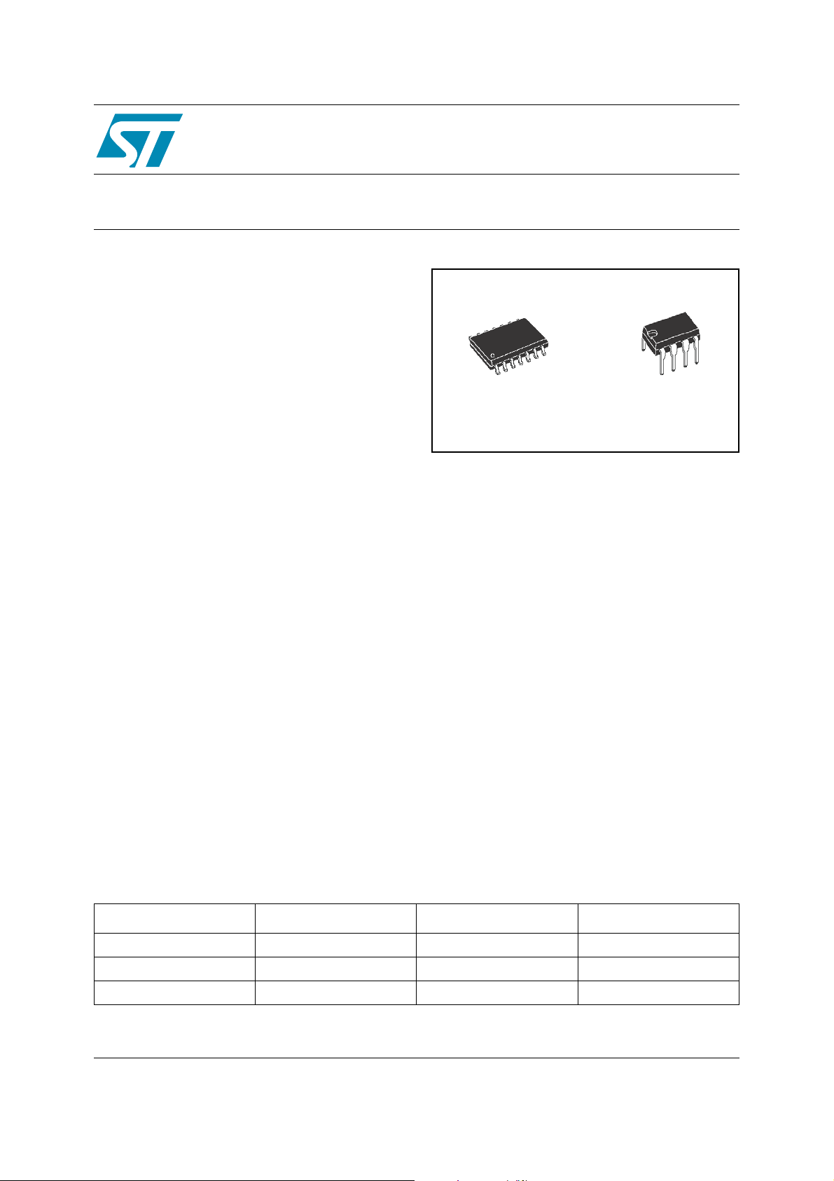
CC
SO14
TDE1747
DIP-8
This device is essentially blow-out proof. Current
limiting is available to limit the peak output current
to safe values.
Adjustment only requires one external resistor. In
addition, thermal shut down is provided to keep
the IC from overheating. If internal dissipation
becomes too high, the driver will shut down to
prevent excessive heating. TDE1747 has an open
ground protection. The output is also protected
from shortcircuits with the positive power supply.
The device operates over a wide range of supply
voltages from standard
± 15V operational
amplifier supplies down to the single +12V or
+24V used for industrial electronic systems.
Order codes
Part number Temp range, ° CPackage Packing
TDE1747DP -25°C to +85°C DIP-8 Tube
TDE1747FP -25°C to +85°C SO14 Tube
TDE1747FPT -25°C to +85°C SO14 Tape and reel
.
September 2006 Rev 1 1/17
www.st.com
17

Contents TDE1747
Contents
1 Maximum ratings . . . . . . . . . . . . . . . . . . . . . . . . . . . . . . . . . . . . . . . . . . . . . . 3
1.1 Absolute maximum ratings . . . . . . . . . . . . . . . . . . . . . . . . . . . . . . . . . . . . . . . 3
1.2 Thermal data . . . . . . . . . . . . . . . . . . . . . . . . . . . . . . . . . . . . . . . . . . . . . . . . . . 3
2 Electrical characteristics . . . . . . . . . . . . . . . . . . . . . . . . . . . . . . . . . . . . . . . 4
3 Pin connections and schematic diagrams . . . . . . . . . . . . . . . . . . . . . . . . . 5
4 Typical characteristics . . . . . . . . . . . . . . . . . . . . . . . . . . . . . . . . . . . . . . . . . 7
5 Typical applications . . . . . . . . . . . . . . . . . . . . . . . . . . . . . . . . . . . . . . . . . . 10
6 Waveforms . . . . . . . . . . . . . . . . . . . . . . . . . . . . . . . . . . . . . . . . . . . . . . . . . . 12
7 Package mechanical data . . . . . . . . . . . . . . . . . . . . . . . . . . . . . . . . . . . . . . 13
8 Revision history . . . . . . . . . . . . . . . . . . . . . . . . . . . . . . . . . . . . . . . . . . . . . . 16
2/17
TDE1747 Maximum ratings
1 Maximum ratings
1.1 Absolute maximum ratings
Table 1. Absolute maximum ratings
Symbol Parameter Value Unit
V
V
P
T
oper
T
STG
1. 60V, t ≤ 10ms
Supply voltage
CC
VI
Input voltage 50 V
Differential input voltage 50 V
ID
I
Output current 1 A
O
Power dissipation (TA = +25°C)
tot
Operating Free–air Temperature Range – 25 to + 85 °C
Storage temperature range – 65 to + 150 °C
Internally Limited W
50
(1)
1.2 Thermal data
Table 2. Thermal data
Symbol Description Value Unit
R
R
thJA
thJC
R
R
Thermal Resistance Junction-ambient 120 °C/W
Thermal Resistance Junction-case 50 °C/W
Junction-ceramic Substrate (case glued to substrate) SO14 90 °C/W
th
Junction-ceramic Substrate (case glued to substrate, substrate
th
temperature maintained constant) SO14
65 °C/W
V
3/17
Electrical characteristics TDE1747
2 Electrical characteristics
TJ = −25 to +85°C, VCC = 8 to 45 V, unless otherwise specified (note 1)
Table 3. Electrical characteristics
Symbol Parameter Min Typ Max Unit
V
I
V
I(max)
Input offset voltage
IO
I
Input bias current – 0.1 1.5 mA
IB
Supply Current (V
High level
CC
Low level
Common–mode input voltage range 2 –
(1)(2)
= +24V, IO = 0)
CC
– 2 50 mV
4
–
–
2
6
4
VCC–2
mA
mA
Short–circuit Current Limit (TA = 25°C, VCC = +24V)
SC
R
SC
R
= ∞
SC
–
480
–
35
50
–
mA
mA
I
= 1.5Ω
Output saturation voltage (output low)
+
– V
I
= + 25°C
J
= + 25°C
A
-
≥ 50mV, R
I
CC
SC
= +24V, TA = + 25°C)
= 0, IO = 300mA, )
–
1.15
–
1.05
1.4
1.3
– 0.01 10 µA
(V
CC–VO
T
V
T
Output leakage current (output high)
I
OL
(VO = 0, V
1. For operating at high temperature, the TDE1747, must be derated based on a +150°C maximum junction temperature and
junction-ambient thermal resistance of 120°C/W for DIP-8 and 100°C/W for the SO14.
2. The offset voltage given is the maximum value of input voltage required to drive the output voltage within 2V of the ground
or the supply voltage.
V
V
V
4/17
TDE1747 Pin connections and schematic diagrams
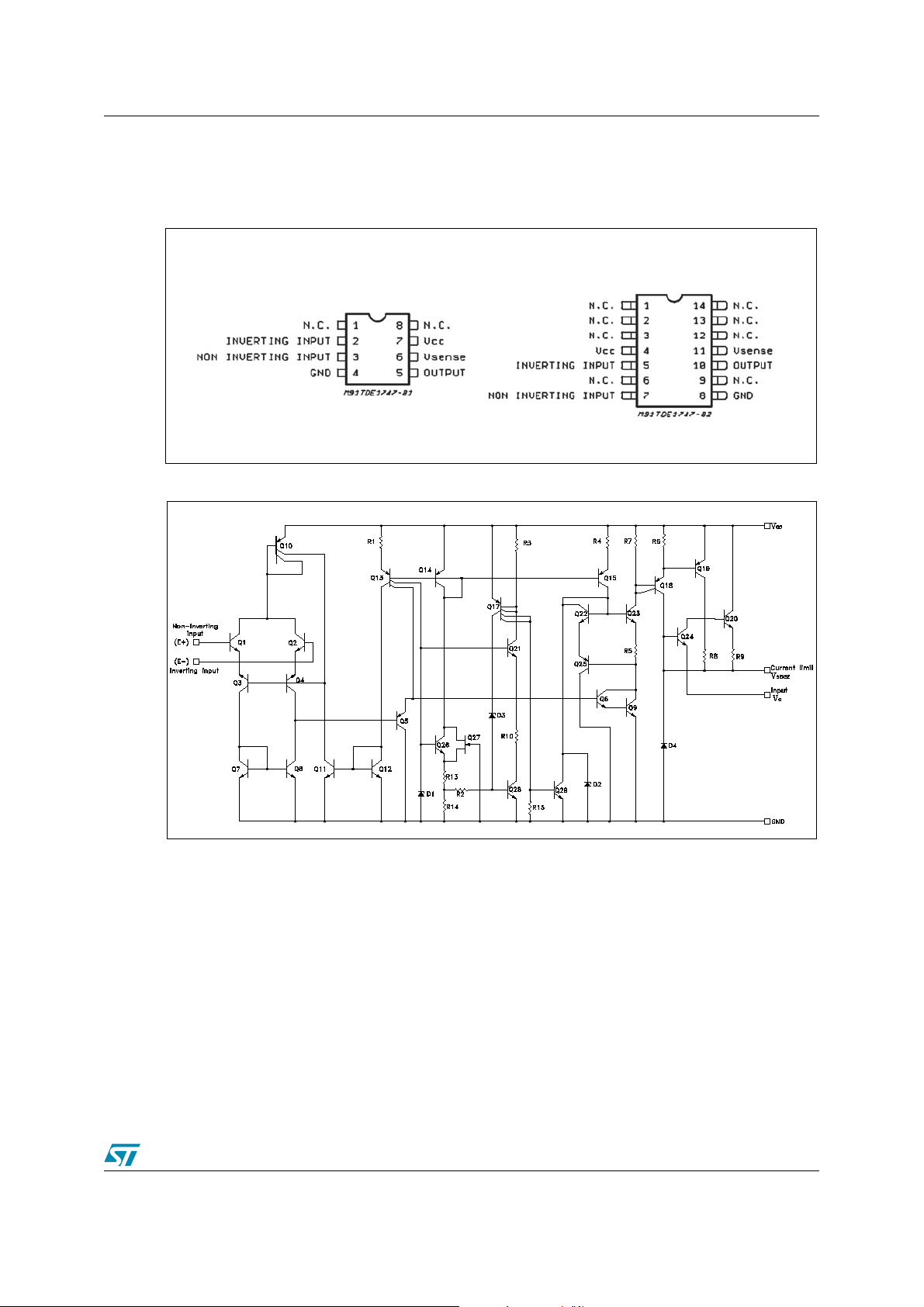
3 Pin connections and schematic diagrams
Figure 1. Pin connections (top views)
Figure 2. Schematic diagram
5/17
Pin connections and schematic diagrams TDE1747
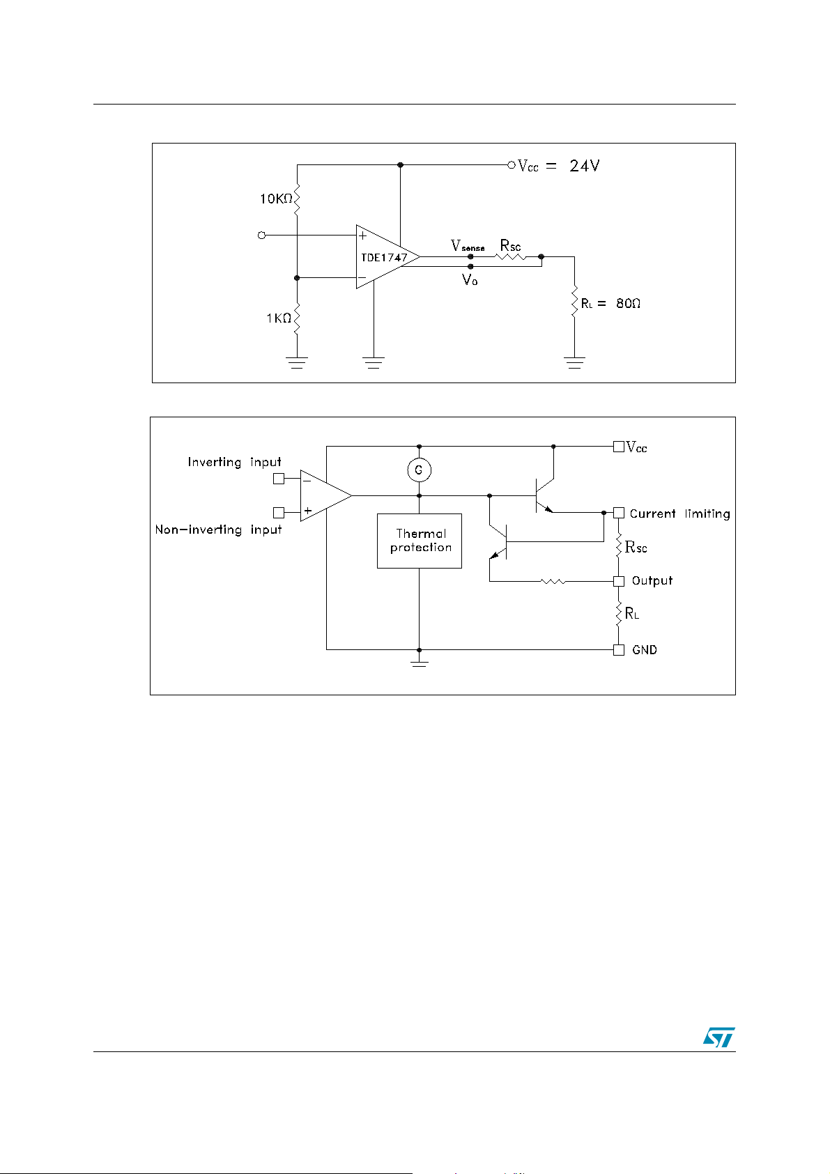
Figure 3. Test circuit
Figure 4. Simplified schematic
6/17
 Loading...