

Features
■ Low side or high side switch configuration
■ 6 V to 48 V supply voltage range
■ Overload and short circuit protections
■ Internal voltage clamping
■ Supply and output reversal protection
■ Thermal shutdown
■ GND and V
■ Adjustable delay at switch on
■ Indicator status led driver
■ +5 V regulated aux. voltage
■ High burst immunity
open wire protection
S
Description
The TDE1708DFT is an integrated power switch
with up to 48 V power supply capability. Two
output configurations are possible:
Load to GND (high side mode)
Load to V
Especially dedicated to proximity detectors, its
internal +5 V supply can be used to supply
external circuits (See also AN495).
(low side mode)
S
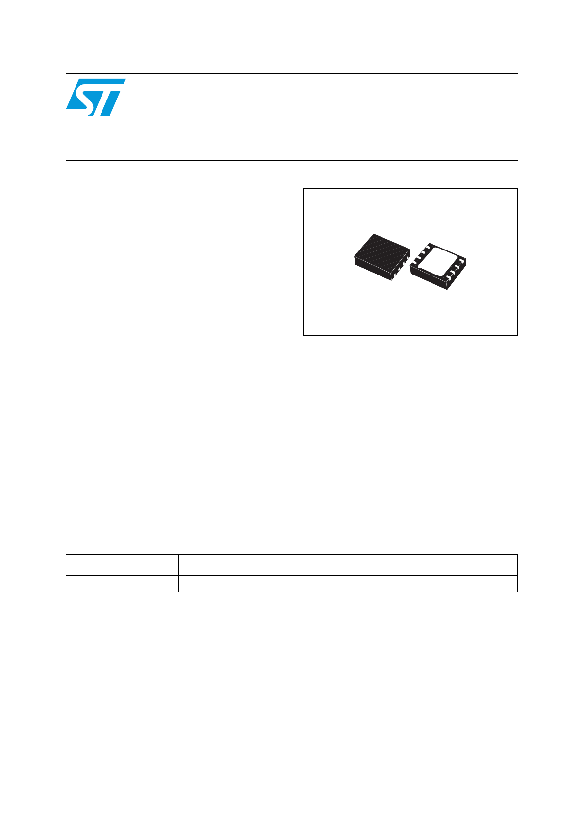
TDE1708DFT
Intelligent power switch
DFN (4x4)
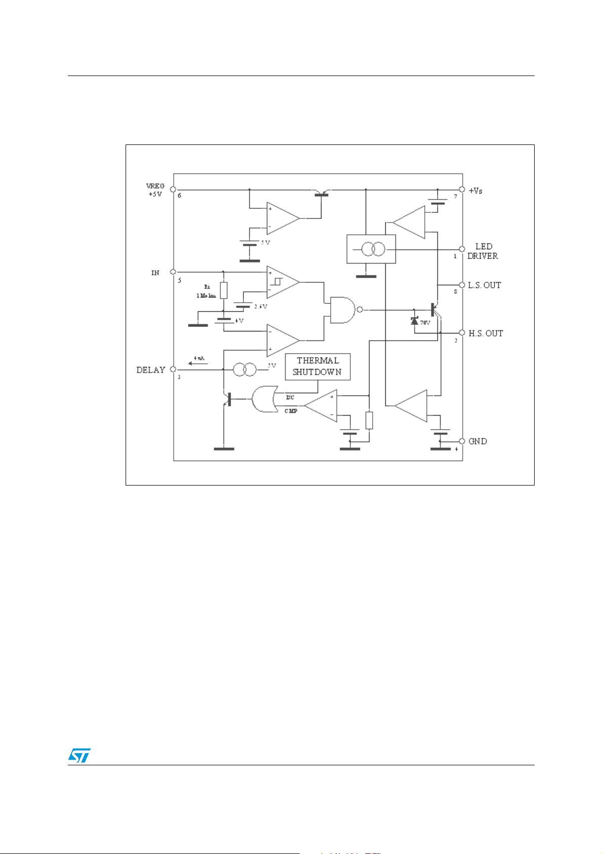
A signal is internally generated to block the In
signal, and prevent activation of the output switch,
as long as an abnormal condition is detected. The
power-on transition, as well as the chip over
temperature and the output overcurrent, concur to
the generation of such signal. A minimum delay of
25 ms (Typ. value) is added to the trailing edge of
such signal to ensure that a stable normal
situation is present when the signal disappears.
The delay (of the disappearance of the block
signal; no delay at its on set) can be further
increased connecting a capacitor between pin3
and ground. It can drive resistive or inductive
loads.
Table 1. Device summary
Order code Temp. range, °CPackage Packing
TDE1708DFT -25 °C to +85 °C DFN (4x4) Tape and reel
February 2009 Rev 4 1/14
www.st.com
14

Contents TDE1708DFT
Contents
1 Block and pin connection diagrams . . . . . . . . . . . . . . . . . . . . . . . . . . . . 3
2 Electrical specifications . . . . . . . . . . . . . . . . . . . . . . . . . . . . . . . . . . . . . . 5
2.1 Thermal data . . . . . . . . . . . . . . . . . . . . . . . . . . . . . . . . . . . . . . . . . . . . . . . 5
2.2 Absolute maximum ratings . . . . . . . . . . . . . . . . . . . . . . . . . . . . . . . . . . . . . 5
2.3 Electrical characteristics . . . . . . . . . . . . . . . . . . . . . . . . . . . . . . . . . . . . . . . 6
2.4 Dynamic information . . . . . . . . . . . . . . . . . . . . . . . . . . . . . . . . . . . . . . . . . . 7
3 Application information . . . . . . . . . . . . . . . . . . . . . . . . . . . . . . . . . . . . . . 8
3.1 Adjustable input hysteresis circuit . . . . . . . . . . . . . . . . . . . . . . . . . . . . . . . 9
4 Package mechanical data . . . . . . . . . . . . . . . . . . . . . . . . . . . . . . . . . . . . 10
4.1 Foot print recommended . . . . . . . . . . . . . . . . . . . . . . . . . . . . . . . . . . . . . 10
4.2 DFN (4x4) mechanical data and package dimensions . . . . . . . . . . . . . . . 11
5 Revision history . . . . . . . . . . . . . . . . . . . . . . . . . . . . . . . . . . . . . . . . . . . 13
2/14
TDE1708DFT Block and pin connection diagrams
1 Block and pin connection diagrams
Figure 1. Block diagram
3/14
Block and pin connection diagrams TDE1708DFT
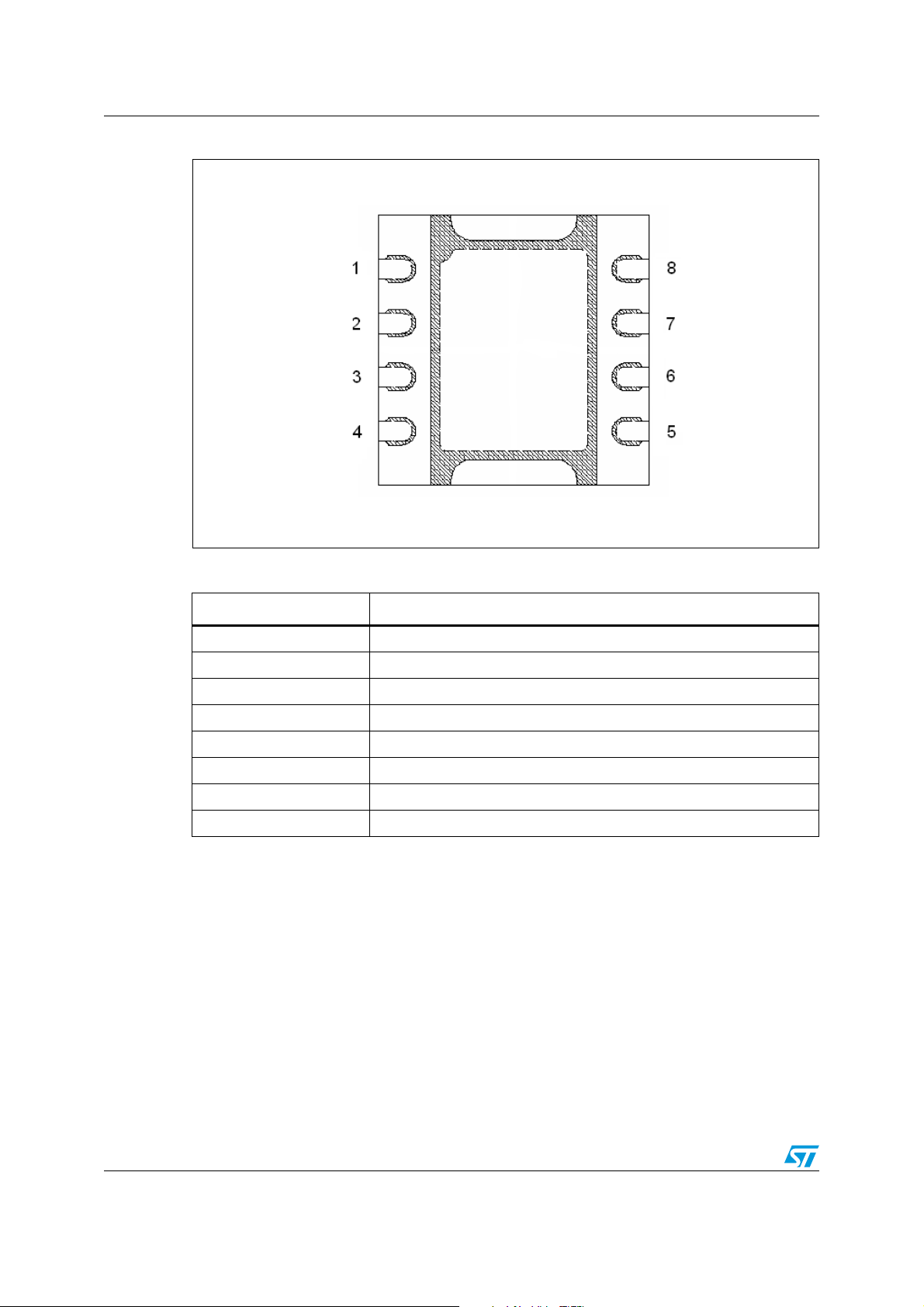
Figure 2. Pin connection diagram (top view)
Table 2. Pin functions
o
Pin N
1 Led driver
2 High side output
3 Delay capacitance source
4Ground
5 Input
6 Reg. voltage source
7 Supply voltage
8 Low side output
Note: Lead frame can be connected to ground.
Function
4/14
TDE1708DFT Electrical specifications
2 Electrical specifications
2.1 Thermal data
Table 3. Thermal data
Symbol Description Value Unit
R
thJA
R
thJC
1. Soldered to a 4 layer board with 4 vias in the pad.
Thermal resistance junction-ambient. (max) 32
Thermal resistance junction-case. (max) 1.2 °C/W
2.2 Absolute maximum ratings
Table 4. Absolute maximum ratings
Symbol Parameter Value Unit
(1)
°C/W
Supply voltage 50 V
S
Supply reverse voltage 50 V
S
Output current internally limited A
Regulated voltage pin 0 to 7 V
Delay cap. source pin 0 to 5 V
Output dif. voltage 55 V
o
Input voltage -10 to 50 V
i
Junction operating temperature Internally limited °C
J
Storage temperature range -55 to 150 °C
Power dissipation internally limited mW
Energy inductive load 100 mJ
i
V
V
V
I
V
reg
delay
V
V
T
T
stg
P
E
o
tot
5/14
 Loading...