

Page 1

AN1290
Obsolete Product(s) - Obsolete Product(s)
®
Application Note
How to Use the TDA911X and Improve Performances
TDA911x Deflection Processors at a Glance
The TDA911x is a family of deflection processors f o r multisync monitors, incorporating horizontal
and vertical processing, geometry correction, dynamic corrections (focus and/or brightness etc.),
DC/DC conversi on and various safety and auxiliary functions. They are entirely controlled through
an I²C interface.
The TDA9112 was designed as an upgrade of the TDA9109/9111, using the same 32-pin shrink
DIP package. The pin-out remains nearly the same in order to simplify new layouts; howe ver some
minor changes were necessary, mainly to pack more functions inside. Those already f amiliar with
TDA9109/9111 will recognize all the functions and operation styles they are accustomed to use.
For low- and medium-range applications where certain sophisticated features are not required,
several different economical versions of the TDA9112 are available: TDA9113, TDA9115 and
TDA9116. Table 1 summarizes their respective features. All versions are pin- and software-
compatible, with minor exceptions
1
.
Recently, the most complete ver sion of the TDA9112 has been upgraded into the higher
performance TDA9112A. Improvements concern mainly geometry and focus corrections, but also
jitter behavior, B+ function, safety and I²C control. The design guidelines provide that the
TDA9112A should operate at once when fi tted in the place of an existing TDA9112 (even if the
ideal I²C register settings may differ slightly).
Section 2: Special Features of the TDA9112A summarizes the improv ements incorporated in
TDA9112A. For a detailed description of each, please ref er to the relevant chapter s.
1. Hard-wired H Moire function of the TDA9115/9116 replaces the Focus/Brightness functions.
16 Septembre 2002 Revision 1.1 1/62
This is preliminary information on a new product now in development or undergoing evaluation. Details are subject to change without notice.
Page 2

Obsolete Product(s) - Obsolete Product(s)
AN1290
Table of Contents
Chapter 1 Main Characteristics of the TDA9112 Deflection Processor Family . . . . . . . . .5
Chapter 2 Special Features of the TDA9112A . . . . . . . . . . . . . . . . . . . . . . . . . . . . . . . . . . . .7
Chapter 3 TDA9112 Family Pin Review . . . . . . . . . . . . . . . . . . . . . . . . . . . . . . . . . . . . . . . . .9
Chapter 4 Horizontal Section . . . . . . . . . . . . . . . . . . . . . . . . . . . . . . . . . . . . . . . . . . . . . . . .11
4.1 Theory of Operation ...........................................................................................................11
4.1.1 Horizon tal Sect ion Structure ................................. ...... ..... ................................................. .................11
4.1.2 Digital Sync Detec tio n .......................... ...... ...... ..... ................................................... ..... .....................12
4.1.3 Composite Sync .................................................................................................................................12
4.1.4 Voltage-controlled Oscillator ..............................................................................................................12
4.1.5 PLL1 ..................................................................................................................................................13
4.1.6 Free-running Frequency and Range ..................................................................................................13
4.1.7 Frequency Precision ..........................................................................................................................14
4.1.8 PLL1 Inhibition ...................................................................................................................................15
4.1.9 Frequency Change Speed Limitation .................................................................................................16
4.1.10 PLL2, Duty Factor, ON/OFF ...............................................................................................................16
4.1.11 Soft-start ............................................................................................................................................17
4.1.12 Output Stage ......................................................................................................................................17
4.1.13 X-ray Protection .................................................................................................................................17
4.1.14 Lock-Unlock Detection .......................................................................................................................17
4.1.15 H Moire Cancellation ............................................ ...... ..... ............................................. .....................18
4.2 Application Hints ................................................................................................................19
4.2.1 Minimizing Jitter .................................................................................................................................19
4.2.2 Output Stage ......................................................................................................................................20
4.2.3 Enlarging the Frequency Range ........................................................................................................21
4.2.4 X-Ray Protection ................................................................................................................................22
Chapter 5 Vertical Section . . . . . . . . . . . . . . . . . . . . . . . . . . . . . . . . . . . . . . . . . . . . . . . . . .23
5.1 Theory of Operation ...........................................................................................................23
5.1.1 Structure of V Section ........................................................................................................................23
5.1.2 Ramp Generator and AGC Loop .......................................................................................................23
5.1.3 Frequency Range and Precision ........................................................................................................24
5.1.4 Sync Detection ...................................................................................................................................25
5.1.5 A G C Loop Stability ................................................ ...... ..... ...... ...... ......................................................26
5.1.6 S and C Correction (TDA9112 to TDA9116) ......................................................................................26
5.1.7 Output Stage and Vertical Shift ..........................................................................................................28
5.1.8 Vertical Signal Management in the TDA9112A ..................................................................................29
5.1.9 ON/OFF Function ..............................................................................................................................30
5.1.10 V Lock/Unlock ....................................................................................................................................30
5.1.11 V Moire ..............................................................................................................................................31
5.1.12 V ertical Breathing Functi on (EHT Compens ation) .................................. ...........................................31
5.1.13 Implementing the Breathing Function ................................................................................................31
2/62 STMicroelectronics Confidential
Page 3

Obsolete Product(s) - Obsolete Product(s)
AN1290
5.1.14 Breathing Functions in the TDA9112A ..................................................................................... ..........33
5.2 Application Hints ................................................................................................................33
5.2.1 Coupling to Booster ...........................................................................................................................33
5.2.2 Ripple Rejection .................................................................................................................................34
5.2.3 Vertical Vibration ................................................................................................................................35
5.2.4 Leakage on Cs ...................................................................................................................................36
Chapter 6 Geometry and Focus Control Section . . . . . . . . . . . . . . . . . . . . . . . . . . . . . . . .37
6.1 Theory of Operation ...........................................................................................................37
6.1.1 Geometry Corrections through E/W (PCC) Output ............................................................................37
6.1.2 Tracking with Horizontal Size .............................................................................................................39
6.1.3 Tracking with Horizontal Frequency ...................................................................................................39
6.1.4 Geometry Corrections through HPhase Control ................................................................................39
6.1.5 Tracking with Vertical .........................................................................................................................39
6.1.6 Dynamic Corrections .........................................................................................................................40
6.1.7 Horizon tal Dyna mi c Focus/Brightness ................................... ...... ..... ........................................ .........40
6.1.8 Vertical Dynamic Focus/Brightness ...................................................................................................41
6.1.9 Vertical Dynamic Focus .....................................................................................................................41
6.2 Application Hints ................................................................................................................42
6.2.1 E/W Output Stage ..............................................................................................................................42
Chapter 7 DC/DC Converter Section . . . . . . . . . . . . . . . . . . . . . . . . . . . . . . . . . . . . . . . . . .44
7.1 Structure of the DC/DC Converter and B+ Loop ................... ....................... ......................44
7.1.1 Structure of the Converter Section ....................................................................................................44
7.1.2 External or Internal Sawtooth Configuration ......................................................................................44
7.1.3 B+ Output Polarity ..............................................................................................................................45
7.1.4 Soft-start ............................................................................................................................................45
7.1.5 Selecting the Trigger Tim in g ............................................................. ...... ..... ...... ................................46
7.1.6 Structure of the Regulation Loop (Step-up, Current mode) ...............................................................46
7.1.7 Structure of the Regulation Loop (Step-down, Current Mode) ..........................................................47
7.1.8 Structure of the Regulation Loop (Step-down, Voltage mode) ...........................................................48
7.1.9 Structure of the DC/DC Converter (Open Loop) ................................................................................49
7.2 Application Hints ................................................................................................................50
7.2.1 Parasites induced by DC/DC Converter (Timing Selection) ...............................................................50
7.2.2 Frame-top Distortion related to Keystone Correction .........................................................................51
Chapter 8 Miscellaneous . . . . . . . . . . . . . . . . . . . . . . . . . . . . . . . . . . . . . . . . . . . . . . . . . . . .52
8.1 Summary of Safety Functions ............................................................................................52
8.2 Early V Blanking and Lock/Unlock .....................................................................................53
8.3 Application Hints ................................................................................................................53
8.3.1 Using Inhibition Properly ....................................................................................................................53
Chapter 9 I²C Control Section . . . . . . . . . . . . . . . . . . . . . . . . . . . . . . . . . . . . . . . . . . . . . . . .55
9.1 I²C Bus Reminder ...............................................................................................................55
STMicroelectronics Confidential 3/62
Page 4

Obsolete Product(s) - Obsolete Product(s)
AN1290
9.2 TDA9112 Family as I²C Bus Device ........... ........................................................................55
9.3 Receiving Data ...................................................................................................................55
9.4 Sending Data ............................ ...................... ...................... .............................................56
9.5 Register Organization ........................ ........................ ....................... .................................56
9.6 Management of Status Register and Sync Priority ............................................................58
Chapter 10 I²C Bus Control Register Map . . . . . . . . . . . . . . . . . . . . . . . . . . . . . . . . . . . . . . .60
4/62 STMicroelectronics Confidential
Page 5

Obsolete Product(s) - Obsolete Product(s)
AN1290 Main Characteristics of the TDA9112 Deflection Processor Family
1 Main Characteristics of the TDA9112 Deflection
Processor Family
Control
● Control of all functions and status reading through I²C interface (status reading is no t available
with the TDA9115).
● I²C settings take effect during the Vertical Oscillator Retrace for an improved screen aspect.
These parameters can be sent at any moment.
Horizontal
● Dual PLL structure
● Maximum frequency of 150 kHz
● Self-adaptable f requency range from 1 to 4.5 or more
● Improved ji tter control functions
● X-ray protection with digital filtering
● Lock/Unlock output; data also available on I²C bus (except for the TDA9115)
● ON/OFF Output function for Power Management
● I²C control of duty cycle, H-position and H-amplitude values with frequency tracking if required
● Smooth frequency transitions
● Internal soft-start
Vertical
● Constant amplitude, self-adaptive vertical ramp generator
● 50 to 185 Hz frequency range
● ON/OFF Output function for Power Management
● I²C control of V-amplitude, V-position, S- and C-correction amplitudes
● S-correction adapted to normal or super-flat tubes
● Lock/Unlock data by I²C (except for the TDA9115)
● Signal for early V Blanking.
East/West Pincushion Correction and Advanced Geometry Corrections
● Pincushion Parabola generator, with DC coupling possible for H-Size control
● I²C control of Pincushion, H-amplitude, Keystone and Corner corrections
● Corner correction, top and bottom independent, symmetric and asymmetric
— No symmetric corner correction for the TDA9115; no asymmetric corner correction for t he
TDA9113, the TDA9115 and the TDA9116
● H and V compensations of EHV variations (breathing inputs)
● Auto-tr acking of all the corrections above with H-frequency (if required) and H-amplitude
● I²C control of parallelogram and side-pin balance correction
● Auto-tr acking of all geometry corrections with V-amplitude and V-position
STMicroelectronics Confidential 5/62
Page 6

Obsolete Product(s) - Obsolete Product(s)
Main Characteristics of the TDA9112 Deflection Processor Family AN1290
Dynamic Correction
● Auto tracking with V-position and V-amplitude
● Composite Dynamic output (e.g. focus or brightness) providing:
— Horizontal Parabola with I²C control of amplitude and symmetry (except for the
TDA9115/9116)
— Vertical parabola with I²C control of amplitude (TDA9112 only).
● Extra dynamic output with programmable polarity (e.g. separate V focus)
DC/DC Converter
● Control section for DC/DC converter, based on UC 3842 architecture
● Programmable for step-up or step-down configurations
● In step-down mode, control of power P-MOS transistor without tr ansformer, or N-MOS
transistor through tr ansformer.
● Internal soft-start
● Can operate as open-loop converter.
Miscellaneous
● Accepts positive and negative H and V sync signals
● Accepts Composite sync signals with the automatic management of serration pulses
● Sync on Green is not extr acted (this function is avail a ble in ST Video preamps)
● Vertical Moire compensation controlled by I²C programming
● Horizontal Moire compensation (I²C prog ramming), ma y be optimiz ed for combi ned or separate
structure (EHV/Scanning).
— TDA9112/9113/9116: self-contained
— TDA9115/9116: hardwired
● I²C bus can read Sync polarity and status, Lock/Unlock status and X-ray status (except the
TDA9115).
● I²C can reset X-ray status.
Table 1 summarizes the differences between the various family versions.
T a ble 1: Family Differences
Description 9112 - 9113 - 9115 - 9116 -
I²C Status reading (sync status, Lock/Unlock, X-ray) Yes Yes No Yes
Symmetrical Corner Correction Yes Yes No Yes
Asymmetric Corner Correction Yes No No No
Pin 11 function Comp DyCor Hor DyCor Moire Moire/DAC
DC/DC converter with internal sawtooth Yes No No No
I²C programmable DC/DC converter reference Yes Yes No Yes
Internal/Hardwired Moire Int Int Ext Int/Ext
6/62 STMicroelectronics Confidential
Page 7

Obsolete Product(s) - Obsolete Product(s)
AN1290 Special Features of the TDA9112A
2 Special Features of the TDA9112A
The TDA9112A provides features and performances at least equal to those of the TDA9112, with
one exception: the DC/DC converter configuration using an internal oscillator has not been
continued because very few customers used it. Software compatibility is maintained.
The new or improved functions are listed below and details may be found in the relevant chapters.
The most important improvements concern geometry and focus correction.
Control
● 8-bit control of the H-size and H-position. Compatibility with the rest of the family is maintained
since only the LSB is affected.
● A dedicated bit enables the MCU to automatical ly detect whether the circuit present is the
TDA9112 or the TDA9112A.
Horizontal
● In PLL1, now there is a choice betw een 4 values of the charge-pump current , to better opti mize
jitter in relation to the horizon tal frequency.
● The indication of H-freque ncy Unlock can be made twice as fast as pre viously.
Vertical
● The block diagram of S and C linearity corrections has been modified to fit in the “tracking”
feature. As a result, it is possible to adjust amplitude or to switch between the VGA modes
without impairing linearity.
● The law of S correction has been modified, all owing perfect fitting to various types of tubes.
● Further to regular amplitude and centring settings (which maintain ideal linearity and
pincushion correction thanks to the “tracking” feature), the new prescale settings (wit hout
tracking feature) provide better flexibility, for instance to adapt one chassis to va rious tubes.
● New EHT compensation has a two-quadrant sensitivity adjustment (i.e. you can choose the
compensation sign as well). This allows perfect compensation throughout the H-frequency
range.
East/We st Pin Cushio n Correcti on and Advanced Geometry Corrections
● Two new controls of E/W are provided, namely S and W control. Their action is symmetrical
versus center. They leave top, bottom and middle of the screen unaffected:
— S correction inflates th e top 1/4 and defl ates the bottom 3/4 or the opposite,
— W correction inflates top 1/4 and bottom 3/4, or deflates both.
These corrections may help prevent certain distortions related to the DC/DC converter.
● A control bit can disable the tracking of E/W corrections versus H-amplitude.
● New EHT compensation has a two-qua dr ant sensi tiv it y adjust ment, in dependent of t he one for
the Vertical section.
STMicroelectronics Confidential 7/62
Page 8

Obsolete Product(s) - Obsolete Product(s)
Special Features of the TDA9112A AN1290
Dynamic Correction (Focus/Brightness)
● The new composite H/V output can pro vide any signal polarity (concavity up or down; same
polarity for H and V).
● The signal at horizontal frequency, previously parabolic, may be set to any power index from 2
to 4. Indeed the useful range is f rom 2 t o 2.5, to adapt t o v a rious tube s a vailable on the market.
● Because the combination of high power index and phase setting may lead to high transients
during H flyback, means are provided to limit transients.
DC/DC Converter
As previously mentioned, the “Internal sawtooth” configurat ion is no l onger av ail able . Impro vement s
include:
● Choice of the maximum current threshold using pin 16 (Isense): previous 2V is convenient
when implementing a sawtooth oscillator, but the new value 1.2V (same as in UC 384x family)
is better adapted for Isense, as in current-mode step-up converters.
● A new control bit performs the ON/OFF function, independently of Horizontal and with soft-
start.
● In addition to the three possible phases for the DC/DC converter (HOut Up, HOut Down, after
HFlyback), a new option is: triggered with top of H sawtooth, with frequency divided by 2. It
may extend the range of step-up conv erters to higher frequencies. Nevertheless, caref u l
filtering and parasitic suppression will be necessary.
Miscellaneous
● B+ Safety: If the control bit is selected, the DC/DC converter will stop whenever HLock is lost.
Restart will take place in a soft way.
● Internal current sinks: E/W and Dynamic correction outputs (pins 11, 24 and 32) now have an
internal current sink which in most cases makes an external resistor unnecessary.
8/62 STMicroelectronics Confidential
Page 9

Obsolete Product(s) - Obsolete Product(s)
AN1290 TDA911x Family Pin Review
3 TD A911x F amily Pin Review
The main features of the TDA9112, TDA9113, TDA9115 and TDA9116 are described in Table 2.
The additional feat ures for the TDA9112A are given in Section 2: Special Featur es of the
TDA9112A.
Table 2: TDA911x Pin Descriptions (Sheet 1 of 2)
Pin No. Pin Description
1 Receives Horizontal or Composite sync signals (TTL compatible, threshold approximately 1.4V, any polarity).
2 Receives separate V sync signals (same level as pin 1, any polarity).
Warning! The functionality of pins 1 and 2 may be affected by I²C.
3 Provides an early V blanking signal (amplitude 1V, High = Blank) to be ORed with V retrace ; combined with an H
Lock/Unlock signal (amplitude 5V, High = Unlocked).
Warning! Blanking and H Lock/Unlock functions are programmable through I²C.
4 Should be filtered to HGND, it improves H Jitter by filtering the H oscillator peak level.
5 (PLL2 filter) should be filtered to HGND (typical value 22nF), it improves jitter by filtering the level at which the
scanning is triggered.
6 The oscillator capacitor Co (typically 820pF) is connected between Pin 6 and HGND. A sawtooth at H frequency will
appear on this pin.
7 HGND; to be connected to General Ground pin 27 and to the components of H section only.
8 The oscillator resistor Ro (typically 5.2kΩ) is connected between Pin 8 and HGND. Co·Ro sets the free-running
frequency as Fo = 0.1215 / (Co·Ro). Voltage on pin 8 is always the same as on Pin 9.
9 The PLL1 loop filter is connected between pin 9 and HGND: 10nF to HGND, and in parallel: 1.8kΩ in series to 4.7µF
electrolytic. The electrolytic sets the speed of H-frequency change when sending a new video mode; the other
components are critical for H jitter characteristics. Voltage on pin 9 is proportional to H Oscillator frequency.
10 Should be filtered to HGND, it improves H jitter by filtering the DC level for H position. Capacitor on pin 10 also sets
the time constant for soft-start.
11 Output pin for composite dynamic H/V Focus (or Brightness). The waveform on this pin is the sum of two parabolas,
one at horizontal frequency, one at vertical frequency. The internal structure is NPN emitter-follower; a pull-down
resistor (10kΩ) is recommended.
The TDA9113 has an H-frequency parabola only.
On the TDA911 5 and the TDA9116, dyna mi c focus is absent, H-Moire c om pen sation is available in the place. To use
it, connect pin 11 to HGND through a resistor divider with ratio of 1000 to 2000, connect the low side of PLL2
capacitor to the middle point (rather than to HGND).
Warning! In the TDA9116, H Moire is I²C-programmable as either external (available on pin 11) or internal; in latter
case, pin 11 is a DAC with a voltage range between 0 and 5V.
12 H Flyback input, a v oltage compara tor (the base of a NP N transis tor with emitter ground ed). It should be connecte d to
a positive H flyb ac k p ulse; a r esist or con nected in s eries is nece ssary to li mit th e inpu t curre nt to less than 5 mA while
the pulse is positive.
13 Reference voltage, 8V nominal, to be filtered versus HGND. Since there is no reference voltage dedicated to the
14 Output of the op-amp that amp lifies the error si gnal of the D C/DC con ve rter feedbac k loop . Its v oltage sets the curre nt
15 Inverting input of the same op-amp.The feedback elements (typically 1MΩ parallel to 10nF) should be connected
Vertical section, pin 13 should also be used for biasing the non-inverting input of vertical booster through a suitable
resistor bridge.
level (represented by voltage on pin 16) at which the power MOS transistor will switch OFF.
between pins 14 and 15. The op-amp non-inverting input is not available; it is internally biased by a 4.8V reference
voltage, adjustable through I²C (e x ce pt the TDA9115).
STMicroelectronics Confidential 9/62
Page 10

Obsolete Product(s) - Obsolete Product(s)
TDA911x Family Pin Review AN1290
Table 2: TDA911x Pin Descriptions (Sheet 2 of 2)
Pin No. Pin Description
16 When the DC/DC converter is used in the External sawtooth configuration, Pin 16 should receive a sawtooth (less
than 2V peak), either represen tativ e of the curre nt in the switch (current mode) or prov ided b y a n R/C oscil lator (op en
loop). In both cases, the po w er MOS tr ansist or is s wi tched O FF when pin 16 v o ltage e x ceed s one-thi rd of the v olta ge
on pin 14. Biasing Pin 16 with more than 6V will set the so-called “internal sawtooth”, in voltage mode configuration
(TDA9112 only).
17 & 18 High-impedance inputs which control H and V amplitude respectively. Each one should receive an image of the EHT
(for instance, a fraction of the Automatic Beam Limiter voltage) for size compensation versus EHT variations. Both
have the sa me act ive range: 1 to 8V, and sign: amplitude increases when pin voltage increases. The gains of the two
channels have to be separately set to the correct values by external resistive dividers.
19 Presents a DC level equal to Vertical sawtooth negative peak, it should be filtered to VGND to improve vertical jitter.
20 The capacitor on pin 20 s tores the AGC value to maint ain the c on sta nt Vertical Sawtooth amplitude regardle ss of th e
frequency. It should be a 0.47µF non-electrolytic capacitor.
21 Vertical ground. In addition to the main GND on pin 27, it should be only connected to Vertical section components.
22 A 0.15µF film capacitor shou ld be conne cted betwe en Pin 22 and V GND to obtain the Vertical Sawtooth with constant
amplitude (between 2 and 5V).
23 The same sawto oth is available on pi n 23 , buffered and wit h ad jus ta b l e a mpl itu de and offset for the control of vertical
size and position. The middle value of this signal is (3.5/8) of the reference voltage (pin 13). An equal voltage should
be derived from pin 13 through a resistive divider, to bias the Vertical booster positive input.
24 Provides the complete waveform to control Horizontal amplitude, including DC (for H Size, with EHV compensation),
Pincushion, K e yston e and s ymm etric Corner. It has the structure of an Em itter follower; a pull-down resistor (10k Ω) is
necessary. Voltage range is 2 V to 8.5V. The TDA9115 does not have corner correction.
25 High-impedance comparator input for X-ray detection, with 8V threshold. It should be filtered to GND (VGND is
recommended).
26 HOut: open-collector NPN with more than 30mA capability. The NPN is switched OFF (pin 26 High) when the
scanning transistor is to be switched OFF (“Reverse control”). An external pull-up resistor connected to pin 29 is
necessary. Direct control of a bipolar NPN driver is possible.
27 General GND. The general GND track should enter the IC area by this pin, then be connected only to the special H
and V ground tracks.
28 BOut: open-collector NPN, with more than 10mA capability. An external pull-up resistor connected to pin 29 will be
necessary to make the power switch conductive.
Warning! The polarit y should be selec ted b y I²C. By default: High level (NPN OFF) is meant to make the power switch
conductive (adapted for N-type power switches).
29 General supply (10.8 V to 13.2 V, 70 mA). It should be filtered to pin 27.
30 & 31 SCL and SDA for the high-speed I²C bus. Threshold voltage is 2.2V typically.
32 Extra V Focus output, to allow separate H Focus and V Focus channels. It provides a parabola at Vertical frequency.
It presents the structure of an emitter follower and requires a 10kΩ pull-down resistor to GND. Quiescent voltage is
4V.
Warning! The signal polarity may be selected through I²C (Default is: Downwards Concavity ∩).
10/62 STMicroelectronics Confidential
Page 11
Obsolete Product(s) - Obsolete Product(s)
AN1290 Horizontal Section
4 Horizontal Section
4.1 Theory of Operation
4.1.1 Horizontal Section Structure
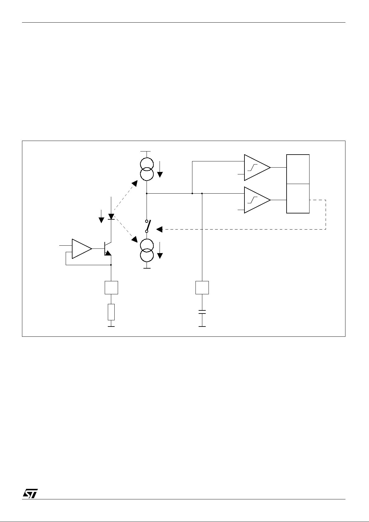
The TDA9112 horiz onta l sectio n is s imilar t o the T DA9109/9111. It includes a sa wtoo th osci llator, a
sync detector, two phase-locked loops (PLLs) and an output st age. Moreover, X-ray protection and
PLL1 lock/unlock detection are provided.
Figure 1: H Oscillator
V9
I8
0.5 x I8
4 x I8
8 6
R0
S
6.4V
R
1.6V
C0
PLL1 locks the oscillator frequency to the HSync frequency, then adjusts its phase, until the sync
pulse coincides with an adjustab le level on the sawtooth. Changing the le v el is us ed to adjust the Hposition.
PLL2 adjusts the phase of the output stage (compensating for the storage time of the H scanning
transistor), until the middle of the H flyback pulse coincides with a predetermined level on the
sawtooth.
The horizontal phase and duty f actor may be adjusted b y I²C programming ( Registers 00h and 01h) .
All voltage values meaningful for the H section (like comparator and oscillator thresholds) are
derived from a common reference voltage (between 7.4V to 8.6V with 8V typical) and keep a
constant ratio with this reference.
STMicroelectronics Confidential 11/62
Page 12

Obsolete Product(s) - Obsolete Product(s)
Horizontal Section AN1290
4.1.2 Digital Sync Detection
The H/HV sync pulse is detected on pin 1 by a comparator with hysteresis, compatibl e with the
standard TTL. It is intended for digital sync only (separate or composite). The IC synchronizes on
the pulse front edge. A pull-down resistor (200 k
Ω) is included.
Sync polarity recognition is performed as follows: The comparator output controls the charge or
discharge of an internal 50pF capacitor with ±0.1µA current . Depending on the polarity of the sync
signal, the capacitor voltage will either drift towards the ground or the 8V supply. A comparison of
capacitor voltage with a 4V threshold indicates the sync polarity. The recognition delay is
approximately 2ms (typi cal) with a minim um value of 0. 75 ms. This w a y, in the event of a Composite
sync signal, vertical sync pulses up to 0.75ms will not be unduly int erpreted as a change in HSync
polarity.
Þ Serration pulses: When they are missing, the inhibition of PLL1 during Vertical sync pulse
(described later) prevents any disturbance of the Horizontal oscil lator. F o r this purpose, the
composite V pulse must be recogniz ed within one horizontal half-period (see Section
4.1.3: Composite Sync).
4.1.3 Composite Sync
In order to extra ct the VSync pulse from the composite signal, the duration of each sync pulse is
compared with the horizontal period. As soon as the durati on of a pulse e xceeds 21% (minimum) of
the horizontal period (30% typical), this pulse is recognized as a VSync pulse.
The VSync duration measurement uses an internal capacitor and a current source that keeps a
constant ratio with Horizontal oscillator current source. Consequently, the system will work as
indicated only if the recommended va lue of 820 pF for oscillator capacitor Co is applied.
Otherwise for instance , when using a higher val ue, at the same frequency, all charge currents will be
higher and therefore the rec ogni tion delay will decrease possibly to less than 21% of the horizontal
period. This would lead to the incorrect detection of the Vertical Sync signal.
See Section 9: I²C Control Section for more information about sync management through I²C
programming.
4.1.4 Voltage-controlled Oscillator
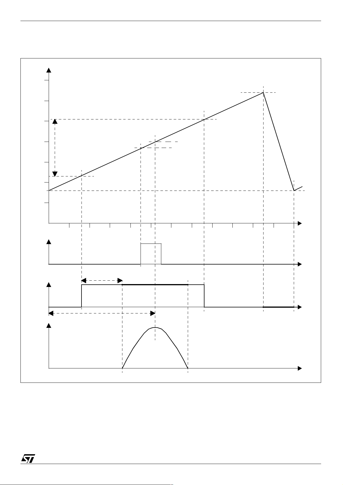
The H oscillator is similar to the one in the TDA9109/9111. See Figure 1 for the schematic diagram
and Figure 2 for w a veforms.
A voltage-follower stage imposes the same voltage on pin 8 as on pin 9, which is the PLL1 output.
The current in pin 8 is then fixed to:
V
8
I
-------=
8
R
0
Current mirroring provides two current sources, with values of 0.5 x I
(“source”) and 4 x I8 (“sink”).
8
Two comparators with thresholds of respec tivel y 1.6V and 6.4V control a toggle that s wit ches ON or
OFF the 4 x I
Supposing this latter source is initially OFF, capacitor C
until the 6.4V threshold is reached. At that moment, the 4 x I
establishing a global discharge current equal to 3.5 x I
12/62 STMicroelectronics Confidential
current source.
8
dV
------dt
dV
-------
dt
0.5xI
---------------- -=
C
3.5xI
---------------- -=
C
will charge at a rate:
0
8
0
current source is switched ON,
8
. Discharge will continue at a rate:
8
8
0
Page 13

Obsolete Product(s) - Obsolete Product(s)
AN1290 Horizontal Section
until the 1.6V threshold is reached; then a new charge phase starts. As a result, the voltage on pin
6 will be a sawtooth with a (6.4-1.6 )V ampli tude and a period of:
∆ThC0x ∆V
Replacing I
exceeds 1.5 mA, the oscillator compon ents will not work in the optimal conditions; mor eover, if
If I
8
at the same time V
by its val ue and taking the reverse , one obtains the theoretical formula:
8
is higher than 6.2 V, there is a risk of saturation of internal circui try. These two
8
æö
---------------- -
èø
èø
0.5xI
f
-----------------------------------------------------------
h
2.286x R0xC0x∆V()()
1
æö
reasons combined led to recommend R
8
V
8
0
1
---------------- -+
3.5xI
8
>4.2kΩ.
with∆V6.41.6
------------------------------------------ -==
10.97x R0xC
– 4.8===
V
8
()
0
Note: All details relative to the oscillator waveform are represented in Figure 2 with: Period = 12 µs,
Flyback duration = 3.2 µs, Duty factor = 50%, Sync pulse duration = 1 µs, Storage time = 2 µs.
4.1.5 PLL1
The aim of PLL1 is to control the osc illator 's fr equency and phase , until the fr ont edge of the H sync
pulse just coincides with a determined (and adjustable) voltage (V
Two current generators (one “source” and one “sink”) are connected to the PL L1 output (pin 9). This
pin is connected to an external low-pass filter, it controls pin 8 voltage through a voltage follower.
● If the front edge of the HSync pulse arrives before the V
φ
current is activated in the interval: this will increase the voltage and the oscillation frequency.
) on the sawtooth.
φ
point on sawtooth, the “source”
● If the V
point on sawtooth arrives before the HSync pulse front edge, the “sink” current is
φ
activated in the interv al, this will decrease the oscillation frequency;
● when PLL1 is locked, there i s a very narrow “source” current pulse just before the V
point and
φ
a very narrow “sink” pulse just after; therefore the voltage on pin 9 remains stable.
may be adjusted by ±0.6V around the a v erage v alue of 3.4V, through I²C programming ( Register
V
φ
01), allowing a cont r ol of t he horizont al phase, up to ±10% of a period. F or an opt im um ji tter, pin 10
should be filtered to GND (no limit on the capacitor value. It also sets the soft-start time constant).
The PLL1 capture range is large enough to synchronize with all incoming sync frequencies.
Normally, both “sink” and “source” currents should be set to 1mA, and the recommended
components in PLL filter are optimized accordingly. Nevertheless, the current value may be
switched to 0.3 mA by I²C programming (Sad16h/d3:2). Jitter may be improved by switching to
0.3 mA at low frequencies and to 1 mA at high frequencies. The default value is 0.3 mA.
In the TDA9112A there are four values for the current that can be selected by I²C programming
(Sad16h/d3:2).
4.1.6 Free-running Frequency and Range
When HSync pulses are absent or at low frequency, the PLL1 output will clamp to 1.33 V, which
corresponds to the free-run frequency (f
f
------------------------------------------ -
0
10.97x R0xC
). From the formula for frequency, we get:
0
1.33
()
0.1215
------------------ -==
R0xC
0
0
STMicroelectronics Confidential 13/62
Page 14

Obsolete Product(s) - Obsolete Product(s)
Horizontal Section AN1290
When HSync pulses are receiv ed, the v oltage on pin 9 will i ncrease until the loc al oscillator mat ches
the incoming frequency. Since the range for pin 9 voltage is between 1.3V and 6.2V, the relative
capture frequency range (ratio of maximum to minimum frequency) is:
6.2
------- -4.77=
1.3
4.1.7 Frequency P recision
All the terms in the f0 equation have a spread. Both voltages are derived from the same reference,
their ratio will remain quit e accurate. In regards to the other v a riables, we have to consider a
tolerance of ±1% for R, ±5 or 10% for C and ±6% for the numerical fact or which incorporates a
current ratio.
Consequently the free-running frequency can vary from ±12 or 17% of the designed value, using
safety marg ins can reduce the usab le relati ve frequency r ange b y 2 x 12% or 2 x 17%; or ±9% if y ou
can afford a ±2% capacitor.
An other consequence of the free-running f requency spread is to mak e the design of a B+ conv erter
more difficult, because in free-running mode, the B+ converter may have to follow the oscillator
frequency down to l o w values. (This may be av oided if fake HSync pulses are sent by t he MCU a t a
convenient frequency, as soon as there is no sync coming through the input plugs.)
14/62 STMicroelectronics Confidential
Page 15
Obsolete Product(s) - Obsolete Product(s)
AN1290 Horizontal Section
Figure 2: H Oscillator Waveform
V
6.4V
5
4V
V
φ
Duty factor
setting voltage
PLL2 Threshold
0
Sync
pulse
V26
Fly
back
t
st
Range for PLL2
5
Forced OFF
1.6V
10 12µs
Forced ON
4.1.8 PLL1 Inhibition
The PLL1 operation remains undisturbed if one (an d only one) sync pulse front edge arriv es in each
horizontal period, in phase with the V
sync pulse, this condition is no longer fulfilled during Vsync, when there are no serration pulses.
point on each sawtooth. In the event of a composite digital
φ
STMicroelectronics Confidential 15/62
Page 16

Obsolete Product(s) - Obsolete Product(s)
Horizontal Section AN1290
When PLL1 endures this sev ere di sturbance , it requires some time to reco v er the proper phase. As
this could entail a visible distortion on top of the screen, the TDA9112 has been provided with a
PLL1 inhibition fe ature: th e two current sour ces of PLL1 will be turned OFF during the Vsync pulse
and 2 complete lines later. Internal inhibition is activated only by the Vsync pulse extracted from
composite sync.
This features may be disabled through I²C programming (Sad16h/d1).
4.1.9 Frequency Change Speed Limitation
It is well-known that when receiving a new horizontal frequency, PLL1 should not synchronize
immediately with the new frequency, especially when it is lower than the former one. Otherwise the
horizontal scanning tr ansistor w ould conduct for a longer period of time, while the v alue of B+ w ould
not have ti me to de crease to its newly assigned lower value. This would lead to excessive current
and voltage and possibly destroy the transistor.
In the TDA9112, the PLL1 changing speed has been limited to a safe value.
Warning! This limitation is ineffective when imposing a frequency jump by switching Ro or Co.
4.1.10 PLL2, Duty Factor, ON/OFF
Supposing the oscillator is loc ked to the Hsync pulse, then PLL2 controls the H scanning tra nsi stor
so that the flyback takes place at a definite point on the sawtooth. (Refer to Figure 2.)
For this purpose, a positive flyback signal must be sent to pin 12, which is connected to a voltage
comparator with a thr eshold of one V
other possibilities, pin 12 may be connected to a secondary of the scanning transformer through a
current-limiting resistor. In order to allow lower values of the limiting resistor, and therefore faster
transmission of the flyback data, the maximum input current into this pin has been increased to
5mA.
The reference point for PLL2 is the middle of the flyback pulse (as seen on pin 12). PLL2 will
manage to make it coincide with the 4V point on the sawtooth.
PLL2 is a classical charge pump PLL. Its output (pin 5) must be connected to a capacitor as a lowpass filter. For the entire fl ybac k puls e durat i on, one of th e tw o 0. 15-mA internal curr ent gen erat ors
connected to pin 5 will be activated:
● the source current, when the ramp voltage is lower than 4 V,
● the sink current, when the ramp voltage is higher than 4 V.
With the flyback pulse centr ed on the 4V point, the capacitor will receive a null global charge for
each period.
The capacitor value is not critical (22nF for good jitter). With a low capacitor value, PLL2 will more
rapidly recover of any change in the H transistor storage time caused by a black/white video
transition. This will mini mize the corresponding distortion of vertical lines.
, and to the Ground through a 20kΩ (typical ) resistor . Among
BE
The Pin 5 voltage directly controls which point on the sawtooth will trigger the scanning transistor
switching OFF. The possible range for pin 5 is between 1.6V and 4V, allowing a transistor storage
time between 0 and:
t
Similarly, the scanning transistor ON state is triggered when the oscillator sawtooth reaches a
determined voltage; the offset between OFF and ON voltages is constant (adjustable by I²C). As a
result, the TDA9112 will maintain constant duty factor, regardless of PLL2 voltage variations . The
typical Duty factor range is between 30% and 65% and is selected through I²C programming
(Register 00). This is the OFF duty factor, i.e. the ratio of the OFF drive time to the total period.
16/62 STMicroelectronics Confidential
æö
0.438x T
èø
æö
èø
–
h
flyback
---------------------2
Page 17

Obsolete Product(s) - Obsolete Product(s)
AN1290 Horizontal Section
Hex code 00 corresponds to a 65% duty factor. This is the default value at start-up, in order to
minimize the stress on the scanning transistor.
4.1.11 Soft-start
The TDA9112 is equipped with a self-contained soft-start. When switching ON, HOut will remain
inhibited until the supply voltage ramps up to more than 8.5V. Afterwards, the initial duty factor will
progressiv ely d ecrea se f rom 85 % to 65 % (t he scannin g t r ansist or wil l be contr olle d OFF for 65% of
the period), then to the v al ue that has bee n set through I²C progra mming. The same ev ents will take
place in the reverse order when the supply ramps down through a 6.5V threshold (t hresholds for
TDA9112A: 8.0V and 6.8V).
The time constant that controls the soft-start is the charge rate of H-positi on capacitor on pin 10.
The soft-start is effectiv e when swit ching ON and when resett ing the HOut inhib ition. It als o controls
the duty factor of the DC/DC converter (except in the so-called “internal sawtooth, voltage mode
configuration”). For more information, refer to Se ction 7: D C/D C Converter Se ction.
4.1.12 Output Stage
The drive signal f or the H scanning transistor is available on pin 26, which is connected to the
collector of the output NPN transi stor. The transistor is conductive (pin 26 LOW) when the H
scanning transistor is t o be ON and vice-v er sa. Pin 26 sh ould be connected t o the supply th rough a
pull-up resistor . Of cour se, some ki nd of driver st age is mandatory to control the scanning tr ansistor
base.
The saturation v oltage on pin 26 (less than 0. 4V f or 30 mA) is lo w enough to all ow d irect control of a
bipolar driver . Ne v ertheless and for ot her reasons we recomme nd keeping an A C coupling bet ween
pin 26 and the driver. For more information, refer to Section 4.2.2: Output Stage.
The output transistor is forced ON during the negative slope part of the sawtooth. It is forced OFF
during flyback (as seen on pin 12), and this safety function has the priority over any other control.
The goal is to prevent the scanning transistor from turning ON again, while it still sustains the high
flyback voltage.
4.1.13 X-ray Protection
Pin 25 is a comparator with 8V (typical) threshold for X-ray detection. A voltage higher than 8V on
pin 25 will stop H scanning (and the DC/DC converter as well). This situation will last until some
Reset takes place, for instance by switching the supply voltage on pin 29, OFF and ON again
(resetting threshold: 6.5V typ at supply fall-down).
In fact, once the voltage on pin 25 exceeds 8V, it must remain at this value for 2 lines befor e the Xray safety is triggered. This digital filtering provides a protection against very short parasitic
voltage, affecting pin 25, due for instance, to an arcing of the tube.
It is possible to read the current state of X-ray protection through the I²C bus. It is also possible to
reset it in the same way (Sad16h/d7).
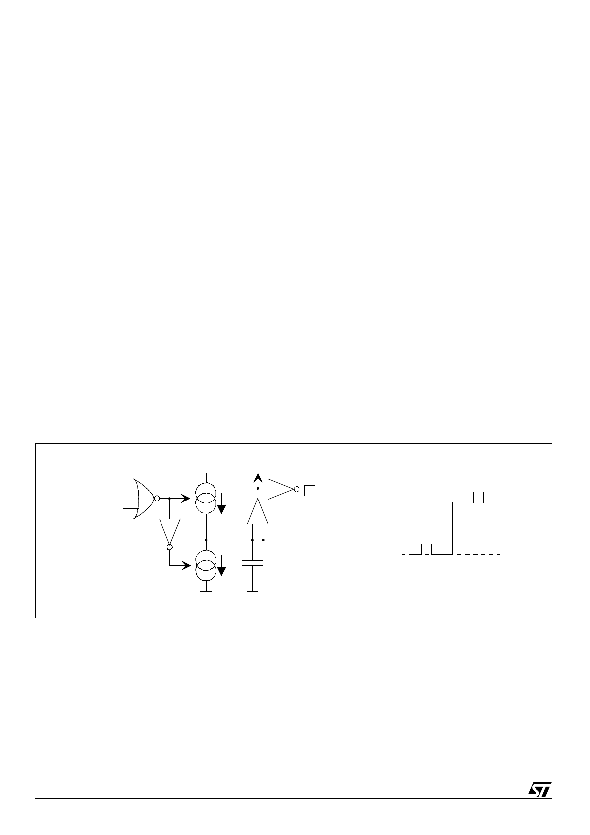
4.1.14 Lock-Unlock Detect ion
Remembering how the PLL1 works with two current generators (one sink and one source), it
appears that when PLL1 is loc k ed bot h genera tors ar e OFF almost al l t he time; when out of phase,
one generator will be ON f or part of the period. When frequencies differ, one gen erat or or the other
will be ON for approximately half the time (mean value).
This is used to build a lock- unloc k detector (Figure 3) where a gate output is LOW whenever one of
the current sources is ON. It controls very low charge and discharge currents to an internal
capacitor. The capacitor voltage will take a value of approximately 8V when PLL1 is locked, and
STMicroelectronics Confidential 17/62
Page 18
Obsolete Product(s) - Obsolete Product(s)
Horizontal Section AN1290
approximately 4V when it is unlocked. The last elements are an internal comparator referenced to
6.25V (with hysteresis) and a CMOS inverter ; you will find on its output pin 3 a HIGH state when
PLL1 is unlocke d. The same data can also be read in the IC through the I²C bus. Nevertheless, a
Read request is necessar y in this case.
There may be an ill-defined state and erratic pulses may appear during Lock
↔ Unlock transitions,
mainly when oscillator f requency approaches Loc k state . The reasons f or this are basic and cannot
be avoided. To pre vent malfunctions, provide an external supplementary delay. Since the delay is
external, it can be made longer f o r the Unlocked
pulses), while being kept very short for the opposite Locked
→ Locked transiti on (thus avoiding the parasitic
→ Unlocked transition, when
emergency measures should be triggered in a short time.
Because some customers asked for a shorter reaction time to transition Locked
→ Unlocked, the
TDA9112A pro vides an option through I²C progr amming (Sad1Fh/d2) for a dela y divided b y two . Be
aware that as a conseque nce, a very long composite VSync signal wit hout serration pulses could be
unduly interpreted as a loss of locking.
Further to this indication, as soon as an Unlock state is detected, the oscillator frequency change
rate is decreased. When switching from High to Low frequency, the B+ regulation loop will have
enough time to decrease the B+ value accordingly, thus preventing th e destruction of the scanning
transistor by overcurrent and overvoltage. According to the typical application schematic, the
frequency will be reduced by approximately 0.1 kHz/ms.
Since pin 3 is also used for V b lanking, levels on pin 3 are defined as follows:
● approximately 0V: locked, not blanked
● higher than 5V: unlocked
● the blanking signal adds to Lock/Unlock level (+1V if Blanked).
The Lock/Unlock signal is availab le only if selected through I²C programming (Sad16h/d0).
Figure 3: Lock/Unlock
To I²C
6.25V
3
1V = Lock, Blank
0V = Lock
6V = Unlock, Blank
5V = Unlock
I
SINK
I
SOURCE
8V
4.1.15 H Moire Cancellation
The Moire phenomenon only takes plac e on color screens and when dis playi ng grey areas resulting
from an alternation of black and white dots.
It may happen that the succession of black and white dots presents a pitch which is very close to
that of the TV screen. If in an are a of t he sc reen, th e whit e dots fall exactly on the tube pi xels, then,
at some further distance, they will fall exactly between the pixels. The result will be a succession of
bright and dark stripes with an approximately v e rtical direction. The nearer t he dot pi tch to t he tube
18/62 STMicroelectronics Confidential
Page 19

Obsolete Product(s) - Obsolete Product(s)
AN1290 Horizontal Section
pitch, the wider the stripes (however, if the dot arra y is not uniform, the basi cally vertical stripes will
be strongly distorted).
Please notice that if the succession of dots is shifted horizontal ly b y half a pix el, the dark and bright
stripes will be exchanged. This pro vides a way to compensat e the H Moire: by artificially introducing
an horizontal jitter with an amplitude of half a pixel, any point on the screen will be successively on
a dark then bright stripe. As a result the eye will see medium brightness everywhere.
Since Moire can also appear with other less simple combinations of dots and pixels, the setting of
the Moire cancellation must be left to the end user for optimum results.
A self-contained H-Moire cancellation system is available on the TDA9112: an internal logic circuit
provides a series of pulses related to H freque ncy with an adjustable amplitude through I²C
(Register 02). After a co nvenient attenuation, this pulsed v oltage wil l modul ate the voltage on PLL2
capacitor , introducing the r equired artificial H jitter . The phase of this jitter is re vers ed for e v ery other
frame, in orde r to make it less noticeable.
This Moire cancellation sy stem can b e used f or any t ype of monitor ( be it common or se parat e EHV
and H scanning). Two modes can be selected through I²C programming (Sad02h/d7). In the event
of a “common” structure, better results will be obtained when set to 0, while 1 is mandatory with a
“separate” structure. If Moire is not needed, the level must be set to 0 through I²C programming.
On the low-cost TD A9115 version, the Moire compensation is av ailable on pin 11 rather than being
applied internally. First, the pulse amplitude of pin 11 must be divided in a ratio of 1000 to 2000 with
a resistor bridge referenced to HGND. Then connect the low-side end of PLL2 capacitor (formerly
grounded) to the medium point of res istor bridge. This wa y, the compensation pulses will be applied
to pin 5 through the capacitor.
The TDA9116 provides either internal or external compensation which is selected by I²C
programming (Sad16h/d3:2). When internal compensation i s selected, pin 11 becomes a 7-bit D A C
with a span between 0 and 5 V.
4.2 Application Hints
4.2.1 Minimizing Jitter
The TDA9112 provides low intrinsic horizontal jitter, but some care must be taken not to spoil its
naturally good performances. Since all horizontal timings are based on the comparison of the
oscillator sawtooth with various DC levels, all these voltages should be kept perfectly clean. Let us
make a “rule-of-thumb” calculation: if the oscillator sawtooth amplitude: 4.8V, corresponds to 7/8 of
the period, then a 1mV parasitic voltage on either the sawtooth or one of the DC levels will induce:
31778 x (7/8)/4800 = 5.8 ns of jitter in VGA, which is an unacceptable value.
Here are some basic precautions to obtain the best ji tter value:
● First, care should be taken not to corrupt the incoming sync pulse. Typically, it will have some
20ns transition time and an 5V amplitude. In these conditions, adding a 0.25 V amplitude
parasitic voltage (ground ripple for instance) will cause 1ns of jit ter on the incoming sync.
Similar considerations apply to Hfly pulse, which is not very fast.
More precisely, we can consider that the components of the PLL1 fil ter hav e been optimiz ed f or
jitter. If jitter is found to decrease when using other values than the ones indicated for theses
components, usually the reason is that the input HSync is already jittered; suppressing this
jitter on the HSync input will lead to a jitter performance unattainable before.
● A separate ground connection, tied to pin 7, should be devoted to all horizontal-related
components, i.e. those connected to pins 4, 5, 6, 8, 9, 10, 12 and 13. This connection must be
tied to pins 21 and 27, but it should not carry any other current, especially those not
STMicroelectronics Confidential 19/62
Page 20

Obsolete Product(s) - Obsolete Product(s)
Horizontal Section AN1290
synchronized to horizontal comp onents in frequency and phase, like those in SMPS, B+
DC/DC converters, PWM DACs, etc.
— The ground tr ack should enter the IC area through pi n 27, then go to the v arious gro und pins
(7, 21, which are not connected internally) and to the H- and V-related components and to
no other place.
● A monitor chassis normally includes several switching circuits, like SMPS, B+ DC/DC
converter . ... The high dI/dt value in some wirings of these circuits will induce para siti c v ol tages
in all neighboring loops. Do not neglect some medium power circuits, like B+ converter gate
drive: even with a low current, the dI/dt value may be high. This will result in a local ized jitter
(i.e. only taking place with certain specific settings of the H-position, H-size, brightness, etc.).
● A decoupling capacitor and its connecting tracks constitute a loop where the high dI/dt value
induces voltages. Same for oscillator capacitor Co. These parasitic voltages appear in series
with the capacitor and induce jitter; they wil l be mini mized if the loop (IC pin-capacitor-IC
ground) presents the smallest possi ble area. The loops that include resistors are less critical.
(Nevertheless, it is advisable to keep the connection to R
minimize parasitic capacitance on pin 8).
● The loops emitting parasites obviously should be as small and remote as possible. (SMPS,
DC/DC converter, etc.)
as short and small as possible to
0
A standard filter f or PLL1 (pin 9) includes:
● 10nF to ground;
● in parallel, the series combination of 1.8kΩ and 4.7µF electrolytic.
4.2.2 Output Stage
The output stage is a NPN transistor, the collector of which is available on pin 26. It becomes
conductive when the H scanning transistor is to be switched ON. Pin 26 must be tied to the supply
through a pull-up resistor. With a 30mA sink capability, it can control a bipolar driver.
Most often, “reverse” control is used, with a driver stage as shown in Figure 4.
IC supply
Figure 4: Driver Stage with MOSFET
Driver supply
Transformer
supply
H scanning
transistor
26
27
(A MOS driver is shown. For an application with a bipolar driver, refer to Evaluation Board booklet) .
The followi ng po ints have to be considered:
20/62 STMicroelectronics Confidential
Page 21

Obsolete Product(s) - Obsolete Product(s)
AN1290 Horizontal Section
● Any ripple, non synchronous to horizontal, on the transformer supply capacitor will influence
the H-scanning transistor stor age time and cause supplementary jitter.
● If a MOS transistor is used as driver, its Gate-Source capacitance must be char ged or
discharged at each transition. This gives rise to large current spikes. The corresponding dI/dt
may induce electromagnetic voltages in the H circuitry and disturb H sync or the oscillator; the
effect will be a local ized jitter (taking place f or one precise setting of Horizontal position or one
precise amplitude etc.). In or der to avoid this prob lem, the d istur bing loop s mu st be minimized:
— charging loop: supply capacitor
capacitor.
— discharging loop: gate/source capacitance
● Be aware that during f a st t rans it io ns, th e base c urrent may be high because the transist or ga in
may fall to low values. A series resistor connected to the bases will help to limit the current
spike in pin 26.
● Since very fast tran sitions take place on pin 26, any capacitance tied to this pin should be
avoided because it would give rise to high current spik es which may cause localized jitter.
By the wa y, please notice in this schematic the A C coupling betwe en IC output and driv er stage . The
reason for this is that when the H output is inhibited (for instance, when the X-ray protection is
activated), t he driver stage is supposed to remain fully co nductiv e. This would l ead to high current in
the driver transformer and resistor. AC coupling prevents remaining in this dangerous state: if a
permanent inhibition takes pla ce, t he driver s tage will soon be OFF and the scanning tr ansistor also
remains OFF because of the transformer coupling.
4.2.3 Enlarging the Frequency Range
If the frequency range is considered too tight, a very simple modification can enlarge it.
In a given application, the frequency is proportional to the voltage across Ro. Voltage on pin 8 may
vary between 1.33V and 6.2V.
If Ro is ref erenced to a Vext v oltage source inst ead of GND, the relative frequency range, pre viously
(6.2 / 1.33), becomes (6.2-Vext) / (1.33-Vext), which might prove mu ch higher.
→ NPN → gate/source capacitance and back to supply
→ PNP and back to source.
For practical implementation, just follow the schematic diagram shown in Figure 5, and use the
equivalent res ist ance and voltage values to determine the frequency range.
Figure 5: Enlarging the Frequency Range
Proposed Schematic
8
R
Ra
Rb
13
Ra Rb
Equivalent Circuit
R
Vext
Vext = Href x Rb/(Ra+Rb)
8
STMicroelectronics Confidential 21/62
Page 22

Obsolete Product(s) - Obsolete Product(s)
Horizontal Section AN1290
4.2.4 X-Ray Protection
The X-ra y protect ion is lat ched; once t riggered b y a v ol tage higher than 8V, it stops t he IC operati on
until it is reset by switching the monitor OFF and ON again, or through I²C programming
(Sad16h/d7).
The voltage on pin 25 is always filtered, which makes it rather insensitive to parasitic voltage.
Neve rtheless, an arcing inside the display tube neck may happen to trigger the protection and stop
monitor operation, which is most unpleasant to the user.
In the TDA9112, the risk has been minimized, since the latch will be triggered not earlier than two
lines after an overvoltage has been detected. Nevertheless, it is preferable to maintain the layout
rules:
● connect the filter capacitor very close to the IC; do not create a loop which may be influenced
by a huge dI/dt,
● establish a path for the arcing current that does not cross the main chassis. A well-accepted
disposition is as follows:
— The ground connecti on fr om th e oute r conduct ive paint of the displa y tube shoul d only g o to
the ground near the tube socket: this way, the charges stored inside the tube will not flow
through the main chassis.
— From there, a ground connection should rea ch the chassi s g round, pr eferably near the EHV
transformer, because this transformer usually includes an EHV capacitor, which will also
discharge during arcing.
Warning! If the X-ray filtering capacitor has a high value, when switching OFF the monitor it can
keep a high voltage while Vref decreases. This will unduly trigger and latch the X-ray protection if
not reset by Vsupply (in case of fast ON-OFF-ON).
This problem is not present in the TDA9112A, where the X-ray protection is disabled as soon as
Vcc drops below 10.4 V (typical).
22/62 STMicroelectronics Confidential
Page 23

Obsolete Product(s) - Obsolete Product(s)
AN1290 Vertical Section
5 Vertical Section
5.1 Theory of Operation
5.1.1 Structure of V Section
The vertical section of the TDA9112 remains basically the same as in the TDA9111. It incl udes a
sync detector, a V ramp generator with Free-running and Synchronized modes, an AGC system to
maintain the amplitude of the V ramp constant, and S- and C-corr ection generators.
V e rtical amplitude and position as well as S- and C-corr ection are control led through I²C (Registers
07 to 0A). All important voltages for the Vertical section are deriv ed from the 8V reference voltage
(same as for the Horizontal section), and are defined as fractions of this voltage.
5.1.2 Ramp Generator and AGC Loop
The structure of the complete ramp generator is represent ed in Figure 6.
Figure 6: Vertical Oscillator and AGC
Io-I'o
5V
5V or
7V
2V
1.6V
Vsync
processor
222
VSync
Co
5V
R2
(A)
NoS
R1
V
A
Rs
S
20
Cs
R
I'o
Io
There are two different operating modes, depending on whether a sync pulse is present:
When there is no sync pulse, switch NoS (= No Sync) is closed, and switch S ( = Sample) is open.
Comparison voltage for discharging C
is set to 5V (or more precisely to 5/8 of reference voltage).
o
Because 5V are forced on C
oscillator capacitor C
.
o
, current I'o is null or very small, and only current Io is mirrored to
s
Combined with an “end of discharge” comparator wi th a 2V threshold, this circuitry pro vides a linear
sawtooth, taking place between the 2V and 5V levels. Dis charge takes place through a 500
Ω
resistor switched to ground, and a simple calculation provides:
V
æö
1
-------
ç÷
V
èø
2
With C
Discharge Time =
= 0.15 µF, V1 = 5 V and V2 = 2 V, the discharge time is 69 µs.
o
RxCxLog
STMicroelectronics Confidential 23/62
Page 24

Obsolete Product(s) - Obsolete Product(s)
Vertical Section AN1290
For the calculation of vertical frequency, we can neglect this discharge time and find:
I
F
0
--------------- -=
v
Cx VD
= 100 Hz (typical)
with I
= 45 µA (typical).
0
Neve rtheless, there is a ±20% spread on this current, so that th e same spread must be expect ed on
the free-running frequency (not taking into account the capacitor spread).
When a sync pulse is received, the system switches to synchronized mode. In this mode, the
vertical sawtooth amplitude is maintained constant in relation to the frequency by an AGC loop, as
described below.
The front edge of the first Vsync pulse opens switch NoS and closes switch S for a 13µs sampling
duration. C
The discharge of C
will then charge to the voltage present at that moment on the amplifier output.
s
is only triggered at that moment. At the same time, the discharge threshold
o
switches from 5V to 7V.
Every subsequent sync edge will trigger the sampling and then the discharge of C
always stores the previous sawto oth peak value. V(C
) is then converted to current I'0 by a high-
s
, so that Cs
0
impedance converter using the following formula:
VC
()5–()
I’0 =
s
-----------------------------R
with R = 18 kΩ.
Since C
is charged by I0-I'0, there is a feedbac k effect. If the last sampled voltage was higher than
o
5V, the charge current will decrease, and con v ersel y, so that next peak v alue will be closer to 5V. At
the end of the process, the voltage on C
5V Rx I
will be 5V + (R x I'0), and the sawtooth peak v oltage:
s
'x
--------------------- -
0
R1R2+
R
2
æö
–
ç÷
èø
with R
= 19 x R2.
1
5.1.3 Frequency Range and Precision
V alue I'o may v ary between -3xIo/4 and +2xIo, so that the to tal char ge current presents a tot al r ange
/4 to 3xIo.
of: I
o
Therefore, the frequency range ma y reach a r atio of 12. Ne v ertheless, the upper and lo wer limits ar e
subject to spread and to thermal drift, which considerably reduces the really usable range.
Therefore the guaranteed autosync frequency range is only 50 to 185Hz, with C
includes a ±5% spread for C
.
o
= 150 nF. This
o
24/62 STMicroelectronics Confidential
Page 25

Obsolete Product(s) - Obsolete Product(s)
AN1290 Vertical Section
5.1.4 Sync Detection
This part is best explained after the oscillator section since the sawtooth is used for polarity
recognition as shown in Figure 7 .
Figure 7: Sync Detection
Positive or
Negative sync
6µs 6µs Edge detector
Sampling pulse13µs
Internal sync pulse
Oscillator capacitor (not at scale)
2.8V
2V
Incoming sync pulses are detected by a comparator with 1.6V threshold, which makes it TTL
compatible. Alternately, they may come from the Composit e sync signal via the sync extractor.
Each transition on the Vsync input (posit ive or negative) triggers a very short (6 µs) pulse. The first
short pulse triggers the sampling, then the discharge of C
pulse will be ignored until the sawtooth exceeds the 2.5V threshold (defining a “dead zone” of
0.5 / 3 = 16.7% of the period).
In case the first detected edge proved incorrect (i.e. a sync pulse back edge instead of the front
edge), the ne xt discharge is triggered b y t he fron t edge , regardl ess of the pol arity of the s ync pulse .
This mechanism fails if the sync pulse duration is too long; hence the limit of 15% fo r V sync duty
factor.
2.5V
Reset pulse
, as explained above. Later, any short
o
End of Vsync
When the Vsync pulse disappears, the oscillator capacitor charges up to 7V (with a decreasing
slope of above 5.4V). When the capacit or reaches the 7V lev el, there are no longer any sync pulses ,
switches S and NoS revert to their initial position and the frequency reverts to free-running mode.
STMicroelectronics Confidential 25/62
Page 26

Obsolete Product(s) - Obsolete Product(s)
Vertical Section AN1290
5.1.5 AGC Loop Stability
Like all sampled feedback systems, the AGC loop has a particular instability mode, which require
special attention:
At a first sampling time, the vertical sawtooth peak voltage is compared to the pre-set 5V value. A
corrective current proportional to the difference is added to the charge current of the oscillator
capacitor with the appropriate sign to decrease the voltage difference at the next sampling time.
Nevertheless, if the correcti on is too large, the next voltage difference may pr esent a higher value
with the opposite sign, this will lead to instability.
Referring to Fig. 3, let
causes a voltage change
(t
is the sampling time; charge current is almost cons tant during ts because ts = 13 µs ≤ Rs x Cs)
s
This entails a change -
∆V
be the initial voltage error on capacitor Co, ∆Vo amplified by gain A
o
∆V
on the sampling capacitor:
s
Ax∆V
∆V
∆V
/ R in total charge current, so that the next sampled voltage will be
s
s
------------------ -x
R
t
0
s
-------=
C
s
s
changed by:
∆V
–
---------- -x
R
s
T
------C
Ax∆V0xtsxT
æö
------------------------------------- -
=
–
ç÷
RsxCsxRxC
èø
0
0
where T = vertical period.
If this value is higher than the initial
∆V
, there will be permanent amplitude oscillation. The
0
condition for stability is then:
Ax tsxT()
With internal values A = 20, t
and C
= 150 nF, this leads to T ≤ 29.3 ms (34.6 Hz).
0
------------------------------------- RsxCsxRxC
= 13µs, Rs = 6kΩ, R = 18kΩ, and recommended values Cs = 470 nF
s
1<
0
Although this seems a comfortable safety margin compared to the usual 50 or 60Hz in display
appliances, one must remember that all parameters (excluding T) in the formula possibly have a
spread. For stability, it is better to stick to the recommended component values.
5.1.6 S and C Correction (TDA9112 to TDA9116)
In the TDA9112, S and C corrections are independent. The circuits are similar to the ones in the
TDA9111 and are controlled by I²C programming (Registers 09 and 0A).
The same control principle is used for S and C corrections. Considering the V-oscillator schematic
diagram shown in Figure 6, capacitor C
receives curr ents I0 and I'0 and also two e xtra curr ents: one
0
for S correction, one for C correction.
26/62 STMicroelectronics Confidential
Page 27

Obsolete Product(s) - Obsolete Product(s)
AN1290 Vertical Section
Let us consider C correction as an ex amp le (Figure 8 and Figure 9). Instead of a ramp with a
constant slope (obtained by charging C
increasing slope. For that purpose, we can add a current with constant positive slope to I
5V
2V
0V
Supplementary current to Co for C correction
with constant current), we want to obtain a continuously
0
Figure 8: C Correction
Effect on Co waveform
- I’0.
0
0
Furthermore, if the supplementary current has a null mean value, it will bring a null charge to C
o
within one period. As a result, the C amplitude adjustment will not modify the amplitude and will
have no interaction with the AGC loop.
Furthermore, the supplementary current for C correction is kep t proportional to the oscillator charge
current I
-I'0. This way, for a giv en C-cor rec tion set ting, the relat ive amount of C correction remains
0
constant, regardless of the vertical frequency.
Figure 9 includes two multipli ers. First, the vertical sawtooth (referenced to its medium value 3.5V)
is converted to a current sawtoo th wit h a null mean v al ue and mul tipl ied b y the cont rol curr ent f rom
the C-correction I²C D A C. The control current may ha v e positive as well as negative v alues in order
to allow C correction in both directions. Then the product is multiplied by a current proportional to
charge current (I
obtain the global charging current for C
-I'o) this, in order to ensure frequency independence. Finally (Io-I'o) is added to
o
.
o
The circuit for S correction is very similar , except that:
● the additional current has a bell-shaped waveform, with positive and negativ e slopes
successively (and still with null mean value);
● the S correction is in one direction only.
Thanks to the bell-shaped waveform, the S correction is well adapted to super-flat as well as
normal display tubes.
STMicroelectronics Confidential 27/62
Page 28

Obsolete Product(s) - Obsolete Product(s)
Vertical Section AN1290
In the TDA9112A only, the S and C corrections are very different (see description below).
Figure 9: C Correction Circuit
3.5V
5.1.7 Output Stage and Vertical Shift
The vertical sawtooth undergoes c ertain modifications bef ore r eaching the v ertical output on pin 23:
To begin with, a high-impedance voltage follower transmits the signal without disturbing the
oscillator.
Considering the oscillator, the exponential shape of discharge waveform is ideal for detecti ng the
end-of-discharge threshold because its slope is not too steep. Nevertheless, the following sta ges
have different requirements:
k(Io-I'o)
I²C
Io-I'o
22
Co
● a steep edge is needed on vertical booster input in order to safely trigger the flyback,
● the vertical sawtooth is also used to generate the E/W corr ection waveforms. If no precautions
were taken, an E/W parabola would be generated during the oscillator discharge period. It
would cause a f ast tr ansient at the beg inning of the ne xt v ertical scanning and disturb the top of
the screen.
For these reasons and before transmission to the following stages, the exponential discharge
waveform is removed from vertical sawtooth and replaced by a steep edge. The signal is then
maintained at a constant value until the rising of the positive slope as shown in Figure 10.
After this operati on, the signal is sent to a variable gain amplifier with a typical adjustment range of
4.4dB. The signal with adjustable amplitude is sent to pin 23 for vertical scanning and to the
geometry control stages.
The mean value of the sawtooth on pin 23 is 3.5V. In order to allow vertical position adjustments, it
can be offset by ±0.3V through I²C bus (Register 08). Obviously, this only can work if the booster
inputs and output are DC coupled. In the section referring to “Geometry corrections”, we will
examine how this is used for geometry tracking. For detai ls on coupl ing to Booster, see Application
Hints below.
The TDA9112A offers more sophisticated settings.
28/62 STMicroelectronics Confidential
Page 29

Obsolete Product(s) - Obsolete Product(s)
AN1290 Vertical Section
Figure 10: Vertical Waveform
Waveform on pin 22
Waveform for following stages
5.1.8 Vertical Signal Management in the TDA9112A
The block diagram of the ver tical signal has been greatly modified in the TDA9112A in order to
obtain the following improvements:
● “Tracking” of S and C linearity corrections: linearity of the display will remain unaffected when
changing V size and position;
● Perfect fit of S correction to all tube types;
● No influence of linearity corrections on the E/W corrections;
● Adaptation to various tubes b y I²C only.
The block diagram is represented in Figure 11.
The signal from r amp generator, modified for the suppress ion of par asiti c E/W parabol a, is f irst sen t
to a variable g ain ampli fier (for vertical amplitude setting), then a v ariab le of fset is added f or v ertical
position control.
The resulting Vramp is used to generate the S and C correction signals, and, further, the E/W
corrections. Since t he correcti ons depend only on t he present v al ue of the ra mp (i.e . on the pre sent
value of scanning current), they will remain fixed on the screen while amplitude and position are
adjusted. This is the “tracking” feature.
Adjusting S compensation will not influence the display amplitude if the amplitude setting is
medium, for other settings there will be some influence.
STMicroelectronics Confidential 29/62
Page 30

Obsolete Product(s) - Obsolete Product(s)
Vertical Section AN1290
In the next stage, the ramp and the S and C corrections are added, then a variable gain is applied
together with EHT compensation, which has its own sensi tivity setting. A second offset v oltage and
the Moire compensation are added, and a buffer transmits the signal to the output on pin 23.
Figure 11: Variable Gain and EHT Compensation
3
SCOR
CCOR
VCoGain
VSAG
4V
VMoire
Buffer 23
VPOF
18
22
3.5V
VSIZE
VPOS
One-quadrant
variable gain
Two-quadrant
variable gain
( )²
(Vramp)
To E/W corrections
(Vramp)
x
2
Notice that this section does not have the “tracking” feature. Adjusting amplitude with “After Gain”
VSAG (1D), or position VPOF (1E), linearity as well as E/W will not follow, and the display aspect
will be changed. Therefo re, the correct adjustment process is as follows:
● Set VPOS to medium value, VSIZE to medium value or the preset value found convenient for
end-user commodity;
● Set VSAG and VPOF for t he raster to fill in the screen conv eni ently (f or instance , if se v eral t ube
types are used with same chassis, the settings wi ll be different depending on tube type); set
linearity and E/W corrections.
The aim is that the center of the sawtooth (d ifferent from center of video!) correspond to the
center of the screen and end of the sa wtooth to bottom of the screen. At top of the screen ther e
should be a black stripe corresponding to video blanking!
● From that moment, to preserve good linearity and geometr y, use only VPOS and VSIZE for
final adjustments (including for the various VGA modes).
5.1.9 ON/OFF Function
A condition that disab les H output ( namely suppl ying less than 8. 5 V when ramping up or su pplying
less than 6.5 V when ramping do wn) will also disable the V output . Thresholds are 8 V and 6.8 V for
the TDA9112A. With a normal supply , the Disab le and Enable f unctions can al so be obtained b y I²C
programming (Sad17h/d1).
5.1.10 V Lock/Unlock
The “Vertical Lock/Unloc k” data is avai lable thr ough the I²C b us in Read mode. St rictly speaking and
as already explained, the vertical oscillator immediately locks with the incoming frequency; what
requires a delay is the est ablishment of the correct amplitude. Vertical locking is indicated as
completed when the peak amplitude is within
±50 mV of the assigned 5 V voltage.
30/62 STMicroelectronics Confidential
Page 31

Obsolete Product(s) - Obsolete Product(s)
AN1290 Vertical Section
5.1.11 V Moire
Depending on the definition mode, v ertical amplitude etc ., the v ertical line step ma y be v ery close to
the tube vertical pitch. This will create an arr ay of interference fringes, just as for the Horizontal
section, and a succession of more or less horizontal stripes, successively brighter and darker.
“Vertical Moire causes horizontal stripes” (which may be strongly distorted).
This unpleasant aspect wil l disappear if e very other frame is slightl y v ertically shifted . The to tal shif t
must be approxi mately 1/2 line step. This very small quantity must be set by the user because it
depends on the mode and the amplitude settings.
If the V-Moire control of the TDA9112 is activated, every other frame will be vertically shifted by an
amount that can be set through I²C bus (0Bh), allowing V-Moir e cancellation.
5.1.12 Vertical Breathing Function (EHT Compensation)
In electron tube displays, and especially in monitors, the display amplitude tends to increase when
beam current increases. This ef fect is most ly noticeabl e when there is a common stage f or EHT and
scanning, it depends on how the f eedback voltage is performed:
● EHT may be directly regulated (through a special bleeder inside the EHT transformer). In this
case, when the beam current increases , B+ has to increase to provide the beam energy, and
consequently H width will increase. On the other hand, display height will have an almost
negligible variation.
● Another possibility is to regulate the peak voltage on a secondary of the EHT transformer. In
this case, because of the internal impedance of the EHT generator, EHT will decrease when
beam current increases. This , in turn, increases the scanning efficiency and the display
dimensions (both horizontal and vertical).
In all cases, f or a same scanning current, display amplitude will increase almost proportionally to
the beam current increase. On the Vertical components, the effect is much more visible in the
second case than in the first one . It has been named “breathing” because the whole display se ems
to inflate or deflate.
Since the beam current data is normally availab le from the A utomatic Beam Limiter (ABL), it ma y be
used to compensate the siz e (v ertical and horizontal, as needed). Alt ernatively, the variation of EHT
(avail ab le th rough t he bl eeder) may be used for the same purpose: a description of this system will
be provided later.
Here we describe the Vertical compensation. A similar system is available f or Horizontal (See
Geometry and Focus control).
5.1.13 Implementing the Breathin g Func t ion
In a multi-frequency monitor, there is no direct w ay to change the V sawtooth amplitude by a
constant amount at various f requencies. In the TDA9112 family, pin 18 has been designed for this
purpose (Figure 12).
Usually, in order to make the beam current data available, the low end of the EHT winding of the
flyback transformer is connected, not to Ground, but to a constant voltage (5V or 12V) through a
resistor. When the beam current increases, the voltage drop across the resistor increases, and the
voltage on the connect ion point goes down. Normally, this point is filtered to GND, and its voltage is
representative of the mean beam current .
In the TDA9112, applying a more negativ e v oltage on pin 18 will cause the amplitude of the v ertical
sawtooth to decrease . Thi s w a y, the breathing eff e ct ma y be compensated if a proper f ract ion of t he
ABL voltage va riation is applied to pin 18.
The “breathing” input is active below 8V (like other characteristic voltages in the data sheet, this
value is derived f rom the internal voltage reference and has the same spread) and should not be
STMicroelectronics Confidential 31/62
Page 32

Obsolete Product(s) - Obsolete Product(s)
Vertical Section AN1290
driven lower than 1V. In this area, decreasi ng the voltage by 1V will cause a 2.5% decrease of the
vertical sawtooth amplitude, which normally should be more than enough for compensation.
A resistive network should be introduced between ABL point and pin 18, with a twofold purpose:
● set the bias voltage in the active area between 1 and 8V,
● apply to pin 18 the ABL voltage variat ions with convenient attenuation.
The simplest schematic diagram (but sufficient in most cases) is represented in Figure 12.
Since Pin 18 has a very high input impedance, the attenuation of ABL voltage variations is set by
the resistive divider (R2 with the parallel combination of R3 and R4). In this case, gain is equal to:
||
R3 R4
----------------------------------------
R2 R3 R4
Since the voltage variation on pin 18 is in the range of 1V, the bias of pin 18 mainl y depends on the
R3/R4 ratio and on the voltag e reference (you can use the one on pin 13, or any other st able and
well filtered reference). Choose R3 and R4 to bias pin 18 in the active range, then adjust R2 for
optimal breathing compensation. Manage to have R2 much higher than R1, in order not to disturb
ABL operation: for that purpose you can multiply R2, R3 and R4 by a same factor without affecting
compensation. Finally, verify that pin 18 will always remain in the active range between 1 and 8V.
||
+
()
Figure 12: Principle of Breathing Compensation
EHT DC 5...12V
EHT Transformer
C1
R1
To ABL
C2
R2
R6
R3
R5
R4
Vref
TDA9112
Breathing
Here the ABL voltage appears at the common point of R1 and C1, the time con stant for ABL is
R1 x C1. Other circuitry, like C2, R6, may be added to improve transient operation.
Usually, the optimal compensation amount is not constant in relation to the H frequency. For
instance, if less compensation is needed abov e a certain frequency, switch S may connect an e xtra
resistor R5 in parall el to R4. As a resul t, the gain and bi as v oltage wil l be reduced in th e same ratio.
After R2, R3 and R4 have been tuned for low-frequency compensation, set the value of R5 for
proper compensation in the high frequency range. Because R5 decreases not only the gain, but
also the amplitude, y ou will ha v e to compensate b y increasing t he Vertical Amplitude setting. Chec k
that pin 18 always remains higher than 1V; for that purpose, it is advisable to set the initial bias
(R3/R4)xVref to approximately 8V. Switch S may be a transistor or a diode, controlled by the MCU.
The control of pin 17 for H breathing is similar, but may require a different value of gain and time
constants. Voltage variations on pin 17 may be as high as 2V, check that they remain in the range
between 1 and 8V!
32/62 STMicroelectronics Confidential
Page 33

Obsolete Product(s) - Obsolete Product(s)
AN1290 Vertical Section
5.1.14 Breathing Functions in the TDA9112A
In the TDA9112A, the “gain” of each breathing compensation channel (H and V) may be adjusted
through I²C parameters HEHTG and VEHTG (Regi sters 1B and 1C). The optimization of breathing
compensation is made much easier , since the MCU is ab le to program the “gain” f or each frequenc y
or frequency range.
The gain span is f our times higher th an the fix ed gain of the TD A9112 f amily: twi ce the pre vious gain
with the same sign, and as much with the opposite sign. (The interest of the opposite sign is when
most of the compensation is done insi de the EHT tran sf ormer itself , t he residue may have an y sign,
and still the TDA9112A is able to perform fine tuning).
Two separate inputs (pin 17 for horiz ontal, pi n 18 for v ertical) hav e been retained for the sake of pin
compatibility. You can connect them together and use a single biasing network if distinct time
constants are not needed f or the V and H sections.
Nevertheless, biasing should be modified, since the active range is now between 1 and 6 V. The
neutral point is 4 V (when input is at 4 V, changing the gain does not modify the amplitude). For
instance you can estab lish the resi stive network to obtain 4 V for bl ac k dis play, then adjust the gain
only once to compensate the breathing with the white display. Even if the 4 V bias is not accurate,
the number of necessary adjustment trials and errors will be minimized.
Make sure the 6 V threshold ( including spread) is ne ver e xceeded! You can see in Figure 13 that the
effect would be unacceptable. (The behavior of H breathi ng is si milar).
Figure 13: V Breathing Transfer Characteristics
Relative V Amp Relative V Amp
1
Undefined area
810
TDA9112 Family TDA9112A
1
Undefined area
V18 V18
01 4 6
Undefined area
5.2 Application Hints
5.2.1 Coupling to Booster
We will e xamine a DC-coupled, double-supply voltage application, used for the DC control of the
vertical position (Figure 14).
The booster is one IC from the TD A8172 f amily, which also includes the TD A 8177 or -F, STV 9379A
or -FA and the STV 9302A. For calculation, the IC is considered as an op-amp. (This means that
voltages on pins 1 and 7 always remain equal because of feedback).
STMicroelectronics Confidential 33/62
Page 34

Obsolete Product(s) - Obsolete Product(s)
Vertical Section AN1290
A first design constraint is centering: no current should flow in R4 when the voltage on pin 23
corresponds to the middle of sa wtooth and when Vertical position setting is in middle position (i.e . V
= Vmid = 3.5V on pin 23).
This easily provides the condition:
or,
(Rf is negligible)
--------------------------------------------------
V
⋅
13
R
40aR40bR2
R
40aR40b
----------------------------------- -
R
2
++
+
R
2
4.5
------- -
3.5
V
=
mid
8
------- -
+=
3.5
--------------------- -
⋅
R1R5+
R
1
-------
⋅
R
5
R
5
A second condition is that peak-peak current in R
or,
where V
In practice, R
varies between 2 and 4V, depending on the Vertical Amplitude setting.
23pp
is between 0.5 and 1Ω, this sets the value of R5/R1. The value of (R
4
follo w s. Select the resistors other than R4 in the range of 10k
limit out of pins 13 and 23. (As a compensation f or increased output range, this limitati on is more
stringent with the TDA9112A!)
The eval uation board incorporates the following values which are considered typical:
R
1
For all resistors except R4, preferably adopt 1% precision to have good centering. If centering is
defective and compensated by offset control, linearity will suffer.
5.2.2 Ripple Rejection
V
23pp
----------------- -
=
R
1
R
5
-------
=
R
1
= 12kΩ, R5=R2=5.6kΩ, R
is controlled by peak-pe a k voltage on pin 23:
f
R
4
-------
⋅
I
pp
R
5
IppR
⋅
V
23pp
4
40a+R40b
-------------------- -
Ω, to respect the maximum current
40a
+ R
= 34.8kΩ, R4=1Ω
40b
)/R2
With an improper la yout, the supply current of some othe r stage may cr eate ripple between the loc al
grounds and add parasites to the ra mp signal. As a result, the scanning current may become
distorted. For instance, let us consider the ground side of R4 as the reference and suppose that
ripple affects the local ground of the TDA9112 (represented with a different symbol). The same
ripple will affect pins 13 and 23.
To provide ripple rejection, the r esistor from pin 13 to booster's positi ve input has been divided into
R
40a
and R
. If their common point is filtered to the local ground, the same ripple will affect it.
40b
Therefore a conditi on exists to apply the same ripple amount to both booster inputs and cancel its
effect: the condition is:
R
40b
34/62 STMicroelectronics Confidential
--------------
R
R
1
-------
=
R
2
5
Page 35

Obsolete Product(s) - Obsolete Product(s)
AN1290 Vertical Section
Take care to connect R2directly to R4, without any othe r intermediate connections (like supplies or
filtering capacitors).
Figure 14: Coupling to VBooster
+ Supply
13
Scanning
Processor
23
7, 21, 27
- Supply
5.2.3 Vertical Vibration
In completed chassis, some designers have noticed a vertical vibration of the display, usually for
precise (but not stable) settings of Horizontal position.
R40a
R1
R40b
R2
R5
7
2
3
6
5
4
1
Yoke
R4
This is another effect of parasitic dI/dt's, as already mentioned in the paragraph about jitter
improvement.
Considering the discharge phase of the V oscillator capacitor, the capacitor discharge is triggered
by the pulse, and it stops when the capacitor v oltage reaches the 2V low er threshold. It ma y happen
that the strong dI/dt from a s witching circuit, loc ated near the TD A9112, induces parasitic v oltages in
the loop constituted by the oscillator capacitor, the IC and their connecting tracks . In most cases,
these voltages, which appear in series to the capacitor, will have the shape of very short pulses at
horizontal frequency. If one of these pulses is negative and takes place just before the lower
threshold switching, it may trigger an early end of the discharge and will result in vertical vibration
(see Figure 15).
STMicroelectronics Confidential 35/62
Page 36

Obsolete Product(s) - Obsolete Product(s)
Vertical Section AN1290
Since the discharge time has some spread, and since the parasi ti c frequency may be any of the
horizontal frequenci es in the range , there is no hope to choose such capacitor, to avoid coincidence
between the parasitic pulses and the critical point. The only way is:
● to give minimal area to the receiving loop “capacitor/IC”,
● to maintain minimal area and maximum distance for the loop which emits parasitic voltages.
Figure 15: Vertical Vibration
70µs
><
~5V
2V
5.2.4 Leakage on C
Considering again the schematic of the AGC system and supposi ng that Cs has some leakage
current I
through R
where V
If V
, the charges lost all along period T must be compensated during the sampling time t,
l
:
s
is the voltage on Rs (provided by the amplifier with gain A = (R1 + R2) / R1.
A
is the peak sawtooth voltage, we have ∆VA = Ax∆Vp, and combining the two equations:
p
Early switching
Vsync
s
V
s
VpI
×
IlT
------------ -
C
s
=∆
==∆
×
l
VAt×∆
-------------------- -
RsC
×
R
s
T
---
-------
×
A
t
Ramp with early switching
Normal ramp
s
For instance, at 50 Hz, a 1% variation of output amplitude will result if I
=80nA
l
For that reason, it is recommended to use a good quality film capacitor (rather than an electrolytic)
as sampling capacitor.
36/62 STMicroelectronics Confidential
Page 37

Obsolete Product(s) - Obsolete Product(s)
AN1290 Geometry and Focus Control Section
6 Geometry and Focus Control Section
6.1 Theory of Operation
The input signal f or this entire sect ion (Figure 16) is the vertical sawtooth vol tage , i.e . the diff erence
between the V
amplitude fact or and added t o a shift factor. The w ay this structure allows f ull tr acking of the display
versus amplitude and posit ion settings will be examined later.
Multipliers convert this linear waveform into parabolic and 4th order waveforms. Then, several
variable gain amplifiers build up various combinations of these waveforms. During oscillator
discharge, the sa wtooth on pin 23 immediately assumes the value corresponding to the beginning
of the next scanning, and so also do all waveforms deriving from it. This way, the wav eforms
corresponding to discharge (the so-call ed “parasitic parabola” and the like) will have a very short
duration, and the correspon ding tr an sie nt, whic h other wise wo uld c ause visi b le ef fects in the upper
part of the screen, will benefit from a maximum damping time.
6.1.1 Geometry Corrections through E/W (PCC) Output
(buff ered) voltage and the internal 3.5V voltage reference, multiplied by an
23
Pin 24 provides a signal for all corrections affecting the horizontal amplitude of the display:
● Horizontal size with EHT compensation,
● E/W (Pincushion) correction (a parabola at V frequency with upwards concavity ∪),
● Keystone (or Trapezoid) (a sawtooth with positive or negative slope),
● Symmetric Corner (not in the TDA9115): a 4th degree parabola, positive or negative, which
will affect the corners of the display much more than the medium area. The Corner correction
may be adjusted independently at top and bottom of the display.
The TDA9112A provides additional features (not represented on the block-diagram):
● The sensitivity (and sign) of EHT compensation may be adjusted through I²C programming
(Register 1C)
● Two more signals are provided for symmetrical E/W correction. Both leave amplitude
unmodified at top, middl e and bottom. S correction can inf late le v el 1/4 and defl ate le v el 3/4, or
the rev erse; W correction can inflate levels 1/4 and 3/4, or deflate both (Registers 19 and 1A).
In monitors provided with separate scanning and EHV, the E/W signal should modulate the B+ of
scanning, in those with a combined structure , it should be sent to an inverting amplifier controlling
the diode modulator.
The structure of pin 24 is NPN Emitter follower. It shoul d be loaded by 10k
Ω (minimum) pull-down.
(the TDA9112A has internal pull-down).
All correction wa v eforms (including the DC for HSiz e) are stac ked abo v e a plateau equal to 2V. This
voltage is stable with temperature to allow DC coupling (mandatory if using amplitude adjustment).
Of course, all these corrections are to be set through I²C (Registers 0C to 10). The maximum
ranges are as follows (value is for maximum H frequency if frequency tracking selected):
● H Size: 2.5V range,
● EHT compensation: 0.5V range,
● Pincushion: 0 to 1.5V for minimum HSize voltage, maximum VSize and me dium VPos,
● Keystone: ±0.5V for minimum HSize voltage, maximum VSize and medium VPos,
● Symmetric Corner: ±1.5V for minimum HSize voltage, maximum VSize and medium VPos.
STMicroelectronics Confidential 37/62
Page 38

Obsolete Product(s) - Obsolete Product(s)
Geometry and Focus Control Section AN1290
The designer is responsible in deciding how much the total voltage will affect the B+ or the diode
modulator voltage. Nevertheless, the va rious corrections will always remain in the same rat io to
each other. For information, the design goal is that total HSize variation corresponding to the total
variation of DC component be
( )²
3.35V
Horizontal
Ramp
Figure 16: Geometry and Focus (TDA9112)
±17% of medium size.
H Focus/Brig ht ne ss
Amplitude
V Focus/Brightness
Amplitude
11
Dynamic
Focus/Brightness
( )²
V Focus
Amplitude
E/W
Amp
Top
Symmetric Corner
Bottom
Keystone
HAmpl
H EHV
Comp
(V9)/5
or 1
32
HAmpl
24
Dynamic
Focus
E/W out
Vdc
23
38/62 STMicroelectronics Confidential
Vertical Ramp with
amplitude control
One-quadrant
gain control
Two-quadrant
gain control
Bottom
Top
Asymmetric Corner
Side
pincushion
Parallelogram
Side Pin Bal.
Out
To Horizontal
Phase
Page 39

Obsolete Product(s) - Obsolete Product(s)
AN1290 Geometry and Focus Control Section
6.1.2 Tracking with Horizontal Size
Since pincushion distortion increases with the distance fro m th e centre, it is a natural requirement
that E/W correction increase with HSize. For that purpose, the amplitude of all cor rections should
decrease when the DC component (HSize) increases.
Because the IC is not informed, either of the true value of B+ or of the amount of compensation
required, it was only possible to specify a typical compensation: the Pincushion, symmetrical
Corner and Keystone corrections will increase by 34% when HSize is driven from minimum size to
maximum size (DC component passing from 2.5V to 0V).
With the TDA9112A, the H-amplitude tracking may be disabled through I²C progr amming
(Sad1Fh/d4).
6.1.3 Tracking with Horizontal Frequency
In monitors provided with a “separate” structure (H scanning separated from EHV), H size is
regulated by a feedback loop which maintains constant the ampl itude of the H fly bac k pul se v e rsus
frequency. In this system, just injecting the signal from pin 24 into the feedback loop will provide
adjustments independent of frequenc y.
On the other side, in monit ors pro vided wit h “common” H scanning and EHV, what is needed on the
middle point of the diode modulator, is an adjustment voltage roughly proportional to frequency.
With the TDA9112 family, through I²C programming (Sad08h/d7) you can select corrections on pin
24 to be either constant or proportional to H frequency. In the latter case, the ranges ind icated
above are v al id when V
Under 5V they will remain proportional to V
Þ The voltage on pin 24 corresponding to maximum amplitude (minimum HSize voltage, centre of
the frame, 8V on pin 17) is alwa ys the 2V plate au. When F requency tr acking is selected (when usi ng
a diode modulator), the global E/W signal (including HSize, pincushion, Ke ystone, Corners, EHT
compensation) has a span proportional to (V9/5), as already explained, above the 2V level.
Therefore, the amplifier which controls the diode modulator must be referenced also to 2V. See
Application Hints f or a detailed analysis.
≥ 5V (tracking is not purs ued abo ve 5V t o a vo id a satur ation of t he output).
9
/5. (Remember that V9 is proportional to H frequency).
9
6.1.4 Geometry Corrections through HPhase Control
These corrections, which affect the H position - rather than the amplitude - of the horizontal lines,
are obtained by modulating the assigned position of the H Flyback pulse (approximately a 4V level
on H sawtooth; see PLL2 and Figure 2). Based on the ramp, parabolic and 4th order signals already
mentioned in E/W section, the TDA9112 elaborates an internal modulation signal to obtain:
● parallelogram cor rect ion
● side pin balance
● Asymmetric Corner (top / bottom independent)
(Asymmetric Corner is also availab le on the TDA9112A , but not on the TD A9113, the TD A9115
or the TDA9116)
Of course, adjustment is made through I²C (Registers 11 to 14) .
● Horizontal position is adjusted thr ough PLL1, as already mentioned (01).
6.1.5 Tracking with Vertical
The structure of the TDA9112 family has been established to allow full tracking of all geometry
controls versus vertical position and amplitude adjustments.
Referring to Section 5.2.1:Coupling to Booster, one can easily check that the vertical scanning
current is proportional to V
-3.5V and that it is null if V23 = 3.5V (centre of the screen).
23
STMicroelectronics Confidential 39/62
Page 40

Obsolete Product(s) - Obsolete Product(s)
Geometry and Focus Control Section AN1290
All corrections (Pincushion, Corner (symmetric and asymmetric), K eystone , P arallelogr am, Side pin
balance) are also computed as functions of V
- 3.5V. This means that for a given point on the
23
screen, constant corrections will correspond when changing vertical amplitude and position.
Consequently, the outlook of the display vertical border will remain unchanged when modifying
these adjustments. This is the “tracking with Ver tical” function.
In the TDA9112A, the “tracking” feature also applies to S and C corrections of t he v ertical sawtooth.
6.1.6 Dynam ic Corrections
The TDA9112 provides the following dynamic corrections (e.g. Focus and/or Brightness):
● On pin 11 a composite waveform HVDyCor for Dynamic Focus or Dynamic Brightness
compensation. It corresponds to the sum of two parabolic waveforms with upwards concavity
∪, one at vertical frequency, one at horizontal frequency. Through I²C, you can adjust both
amplitudes (V Focus (Register 06) can be set to 0, but not H Focus (Register 04)) as well as
the symmetry of H parabola (Register 05).
● On pin 32, a parabolic waveform at vertical VDyCor frequency, with selectable polarity through
I²C programming (Register 15).
This flexible architecture allows various combinations, like:
● separate V Focus (positive or negative) and H Focus,
● composite Focus,
● V Focus (positive or negative) and composite Dynamic Brightness.
The TDA9113 has only a Horizontal parabola on pin 11; TDA9115 and TDA9116 provide only the
vertical parabola on pin 32, while pin 11 is devoted to Breathing compensation.
The TDA9112A provides all the features of the TDA9112 and, in addition to these features, on pin
11:
● Both signal polarities may be selected (1Fd1): either upwards concavity ∪ of the composite
waveform with the apex at 2.1V, or downwards concavity
● In order to best compl y with the focus requi rements of modern flat screens, the shape of the H
“parabola” may be continuously varied through a 7-bit I²C register (Register 18), from true
parabola (power index 2) to power index 4, while its amplitude remains basically unaffected.
6.1.7 Horizontal Dynamic Focus/Brightness
The Horizontal Dynamic Focus/Brightness features are available on the HVDyCor pin (pin 11).
In order to provid e a parabolic v oltage synchronous wit h the Horizontal component s, a synchronous
sawtooth voltage is first internally generated with a current source that charges a capacitor. An
internal AGC system maintains a constant amplitude of the sawtooth.
The capacitor discharge takes place inside flyback, through a 500
but not negligible discharge time of 500 ns (typical).
∩ with the apex at 7V;
Ω resistor, which leads to small
The ramp voltage (referenced to its mean value) is then squared to finally provide on pin 11 a
parabolic voltage with upwards concavity
∪ and an amplitude between 1V and 3.5V which is
adjustable through I²C programming (Register 04).
Usually, the amplitude of the HFocus parabola should increase when the HSize increases. For this
purpose, you can select the “Amplitude Tracking” feature through I²C programming (Sad04h/d7).
Because the parabola is obtained by squaring an internal sawtooth, its amplitude will vary to the
squared value of the amplitude setting.
40/62 STMicroelectronics Confidential
Page 41

Obsolete Product(s) - Obsolete Product(s)
AN1290 Geometry and Focus Control Section
During the discharge period, the level of the H Focus signal is maintained to the value
corresponding to the beginning of the ne xt scanning period. This allo ws a maximum amount of ti me
for the damping of the transients which appear during flyback.
At first glance, the HFocus parabola should be symmetric in comparison with the middle of the
displays. Nevertheless, the Dynamic Focus amplifier is normally a Class A amplifier with a highvalue resistive load, and the effect of the parasitic capacitance shunting the load, if not
compensated in the input circuitry, may be approximated by a constant delay. This delay may be
roughly compensated if the HFoc us parabola is shifted in advance, ta king an unsymmetrical
outlook.
The TDA9112 offers two ways to implement this phase shift:
● First, you can choose, through I²C progr amming, the point where sawtooth discharge begins:
either the start or the middle of flyback (Sad05h/d7).
● Second, you can progr am th rough I²C (Register 05) the dissymmetry of the parabola, i.e.
manage to shift its minimum forward or backward by
seeking constant time adv ance, the phase setting will have to be frequency-dependent.
In the TDA9112A, the available output range for H “parabola” has been improved as follows:
Usually the “parabola” is shifted in adv ance to compensate for the dela y in the external class-A
amplifier, this means that maximum amplitude will be reached at the end of H period, which entails
two drawbacks:
● high dynamic range is needed (and the more so because the TDA9112A allows a “parabola”
with degree higher than 2),
● a high-amplitude transient m ust take place to reach the low amplitude at beginning of next
period.
±22% of H period. Of course, if you are
This is a waste when it takes place during flyback, i.e. while video is blanked. For this reason, the
TDA9112A has an I²C bit (Sad1Fh/d0) that pulls down the H signal ahead of normal time, i.e. as
soon as flyback begins. This means that the flat signal at beginning of the H period may be
extended to begin with fl yback.
6.1.8 Vertical Dynamic Focus/Brightness
A parabola at Vertical frequency is built up from the Vertical sawtooth, as already indicated. It has
the same polarity as the Horizontal parabola, a programmable amplitude from 0 to 1V (for typical
VAmp and VPos values) and it will track VAmp and VPos signals.
The sum of H and V parabolas is available on the HVDyCor pin (pin 11). The apex value is
temperature-stable to allow DC coupling to the focus amplifier. The structure is emitter-follower
(requires a 10k
TDA9112A).
Ω pull-down resistor for the TDA9112 family; pull-down is internal on the
6.1.9 Vertical Dynamic Focus
In addition to the pre vious out put, a separ ate VF ocus output is av ailab le on the VDyCor pin (pin 32).
It also has the tracking feature versus VAmp and VPos values. Its amplitude is programmable
through I²C (Register 15) from 0 to 1V (VAmp and VPos typ); polarity is also prog rammable
(Sad15h/d7). The plateau level is 4V. The structure is NPN Emitter-follower, a 10k
resistor is necessary (except for the TDA9112A).
Ω pull-down
STMicroelectronics Confidential 41/62
Page 42

Obsolete Product(s) - Obsolete Product(s)
Geometry and Focus Control Section AN1290
6.2 Application Hints
6.2.1 E/W Output Stage
An output inverting amplifier has been designed to ensure the interface with an E/W diode
modulator (see Figure 17).
Figure 17: E/W Amplifier
Vs=12V
470k
To sub-HSize DAC
3819
To diode
modulator
220p
TIP 122
24
33
Vi
9
1715
18
Here are some explanations on its design.
This is a simplified pow er op-amp with high, sink-only current capability.
Design data: R
If V
is the input voltage and sinc e we have an op-amp, the following relation holds:
i
= 1kΩ, R9 = 470Ω, R38=2.2Ω (negligible)
15
–
19
i
+
VsV
–
-----------------R
17
i
---------- -=
R
VdV
æö
------------------ -
ç÷
R
èø
V
i
18
Vd
or,
V
d
---------- R
19
1
19
1
---------- R
æö
V
---------- -
×
i
èø
R
17
1
---------- -++
R
18
–=
V
---------- R
17
s
On pin 24, a parabolic v olta ge with minim um v alue approximately 2V is available . The pe ak va lue is
approximately 8.5V wit h V Amp , Breathing, Pincushi on, Ke ystone and Corner corrections set to their
maximum value. We must choose the various resis tors so that the output voltage will be
approximately 0V when the input is 2V, and will be at the maximum v a lue when the input is 8.5V.
The maximum output is estimated at 40V for the maximum frequency (to be compared with
approximately 200V of B+) ; less is needed at lower frequencies.
42/62 STMicroelectronics Confidential
The output must be able to go down to near ground when V
æö
0V
=
ç÷
èø
1
æö
---------- -
×
i
èø
R
1
---------- -
++
R
19
17
1
---------- -
R
18
= 2V, therefore:
i
V
s
---------- -
–
R
17
Page 43

Obsolete Product(s) - Obsolete Product(s)
AN1290 Geometry and Focus Control Section
or,
V
s
------ -
R
=
2
The output must go to 40 V when input is 8.5 V, therefore:
40
---------- -
R
19
8.5
×
Combining both equations:
40
---------- -
R
19
or,
R
17
---------- -
R
19
1
æö
---------- -
⋅
17
èø
R
1
æö
---------- -
èø
R
19
×
8.5
V
⋅
S
1
---------- -
++
R
19
17
1
17
---------- -
R
s
–=
17
1–
1
18
---------- -
R
0.975==
---------- -
++
R
V
------------------ -
⋅
2R
8.5
------- -
8.5
--------
2
----------------- -
40
1
---------- -
R
18
V
s
17
–=
V
s
---------- -
R
17
Returning to first equation:
V
s
------ -
= 1
2
æö
R
---------- -
⋅
17
èø
R
1
1
---------- -
++
R
17
19
1
---------- -
R
++= 1
18
R
17
---------- -
R
18
R
17
---------- -
R
19
R
17
---------- -
R
18
0.975++=
We determine:
R
17
---------- -
R
4.025=
18
Now we must choose the value of one resistor out of R17, R18 and R19, the others follow:
Choosing R17 = 270 k
Ω entails R18 = 68 kΩ, R19 = 270 kΩ (nearest normalized values).
ÞPlease notice that the R17/R18 divider applies a bias voltage of 2.4 V to the feedback input ,
which is slightly hi gher than the “plateau” volt age which corr espon ds to the maxim um H-amplit ude .
R
18
----------------------------
12
⋅
R
17R18
+
2.4V=
This is mandatory to ensure that the amplifier output voltage will be approximately 0 regardless of
the frequency when the H-size is set for maximum amplitude.
ÞSince this bias vol tage and the voltage from the IC derive from different s ources, there may exist
some offset between these voltages. This offset might be non- negligi b l e compare d to the tot al E/W
voltage from IC (mai nly at a lo w H frequenc y, when frequency tracking is used). As a consequenc e,
it might be impossible to properly adjust the horizontal amplitude at a low frequency. A convenient
countermeasure is to implement a bias adjustment (sub-HSize) with a DAC and a resistor (470k
Ω
should be convenient). The adjustment is shown in Figure 17.
ÞTake care to provide a pull-down resistor to always keep the output transistor conductive on pin
24! (Not needed with the TDA9112A)
ÞYou will find on the ST Ev aluati on Board a simila r application; e xcept that t he signal f rom pin 24 to
the input passes through an attenuator (R
in gain has been more than compensated by increasing the value of R
constitutes a resistive divider with R33//R37). The loss
34
. This leads to a set of
19
values (to be adapted to specific applications):
= 1 kΩ, R33 = 4.7 kΩ, R37 = 27 kΩ, R17 = 270 kΩ, R18 = 39 kΩ, R19 = 270 kΩ
R
34
STMicroelectronics Confidential 43/62
Page 44

Obsolete Product(s) - Obsolete Product(s)
DC/DC Converter Section AN1290
7 DC/DC Converter Section
7.1 Structure of the DC/DC Converter and B+ Loop
7.1.1 Structure of the Converter Section
The DC/DC converter section has a basic structure very similar to the well-known UC 3842 family,
i.e. current-mode PWM converters. (You can refer to the corresponding datasheet). It includes:
● An oscillator to swit ch the pow er MOS transi stor ON. In fact the horizontal oscillator is used f or
this purpose, ensuring correct synchronization. Triggering can take place at various points of
the period selected through I²C programming (Sad07h/d7 and Sad17h/d3), in order to
minimize the disturbance by switching parasitic voltages.
● An error amplifier, which compares a fraction of the voltage to be regulated with an internal
voltage reference, and amplifies the difference.
The internal reference is approximately 4.8 V (rather than 2.5V as in UC 3842). It may be
adjusted by ±20% through I²C (Register 03), except on th e TDA9115.
● An (Isense) pin (pin 16) which meas ures the c urrent in t he s witch, or rather t he v oltage dr op on
a low-valued series current-sense resistor
● A comparator to switch OFF the power transistor when (Isense) voltage reaches a fixed
fraction (1/3) of the amplified error voltage. For safety, switching OFF will take place anyway if
the voltage on the Isense pin reaches 2V. With the TDA9112A, you can choose by I²C
programming (Sad01Fh/d7) between 2V and 1.2V for switching OFF. (1.2V is best suited for
normal applications, 2V for open-loop converters.)
The duty factor is not li mited and can almost reach 100%. (Nevertheless, after switching OFF, the
power MOS transistor will remain OFF for approximately 300 ns.)
Compared to older circuits lik e the TD A9111, the DC/DC section has been slightly modified to allo w
new applications, like Open-loop control.
7.1.2 External or Internal Sawtooth Configuration
The above description co rresponds to the Current mode, step-up configuration (or to the related
configuration: Current mode, Step-down) and makes use of the external sawtooth of pin 16.
It has distinctive advantages:
● very simple control of the power MOS transistor,
● pulse-by-pul se current lim itation,
● loop stability is easily guaranteed because the converter itself has a first-order frequency
response (as long as operation is i n discont in uous cond ucti on mode , i .e . cu rrent i n the rect ifi er
falls to 0 at each period),
● parasitic voltages generated only at switch-OFF (in discontinuous mode).
On the other hand, remembering that switchi ng is synchronized to the Horizontal section (i.e. a
complete cycle must tak e place within one H period), a lar ge frequency r ange ma y be obtained only
at the expense of higher peak current. This means a larger power MOS transistor.
With the same circuit, it is also possible to implement a step-down, continuous conducti on
converter. In this case, a high-side switch is used. Continuous conduct ion converters are generally
not current-mode, but voltage-mode. The error amplifier output is no longer compared to an image
of the current, but to any sawtooth.
44/62 STMicroelectronics Confidential
Page 45

Obsolete Product(s) - Obsolete Product(s)
AN1290 DC/DC Converter Section
The step-down, continuous conduction converter does not have the advantages of a step-up
configuration, but it is easily adapted to a large frequency range, since the ratio of the regulated to
unregulated voltage is just equal to the duty factor.
Neve rtheless, the slo w f requency res ponse of the step-down voltage mode makes it ill-adapted to
direct modulation by the E/W signal. It may be used with a diode modulator for E/W.
When a voltage-mode structure is adopted, “Isense” input bec omes useless . In t he TDA9112 only,
(I sense) pin (pin 16) is used for programming:
● When its voltage is below 6V, it has a standard operation (Isense),
● When it is higher than 6V (for instance, connecting pins 16 and 13 together), the internal H-
Focus sawtooth is automatically used for the comparison in place of the Isense pin.
7.1.3 B+ Output Polarity
In step-up configuration, with a low-side N-type switch, a positive pulse applied on the gate entails
conduction. The duration of the positive pulse is modulated according to the power requirements.
In step-down, two kinds of high-side switches may be used:
● either a N-type: in this case the same contro l pulse is needed, but referenced to the floating
MOS source; it will be transmitted through a transformer for isolation purposes,
● or a P-type: in this case, direct capacitive coupling of the gate to B+ pulse is possible, which
eliminates the need for a coupling transformer. Still, a negativ e-going pulse is needed to make
the MOS conductive.
For that reason, B+ output pulse polarity may be programmed through I²C (Sad06h/d7).
Of course, the converter Disable function will function regardless of the polarity, i.e. it will either
force output to LOW state if polarity is positive or to HIGH if the polarity is negative.
7.1.4 Soft-start
When switching the supply ON, or whenever quitting the Disable state, the duty factor of BOut will
increase progressively until its normal value is reached. The soft-start controller is the same as for
HDuty, based on the charge of the HPos capacitor. No extra component is needed. The v alue of the
HPos capacitor sets the soft-start time constant.
From the moment the soft- start is triggered, with 0V on HPos capacitor:
● nothing happens until the voltage reaches 1V;
● then HDuty progressiv ely decreas es fro m 85% to 6 5%, with B+ still OFF, unti l the HPos voltage
is 1.7V;
● then B+ duty factor begins t o increase (starting from 0); both duty factors continue to chan ge
until they reach their programmed value.
When the HPos voltage reaches 2.8V, both duty factors are normal. The HPos voltage still has to
reach its steady-state value.
Þ By the way, it is still possible to implement a soft-start circuit with external components, as with
the TDA9111.
Þ The Soft-Start feature is not active in the Internal sawtooth configuration.
Þ The TDA9112A only has a special I²C instruction (Sad1Fh/d6) to enable/disable B+ alone, it is
fitted with its own independent soft-start (with internal time constant) and no soft-stop.
STMicroelectronics Confidential 45/62
Page 46

Obsolete Product(s) - Obsolete Product(s)
DC/DC Converter Section AN1290
7.1.5 Selecting the Trigger Timing
In Internal sawtooth configuration, since the HFocus sawtooth is used for comparison purpose,
conduction of the power MOS tr ansistor is triggered at t he same time as the sawtoot h, i.e. inside th e
flyback pulse (See Section 6.1. 7: Horizontal Dynamic Focus/Brightness for more details).
In External sawtooth mode, depending on the architecture (details below) it may be advantageous
to select the proper trigger point. the TDA9112 family offers three possible trigger points which
may be selected through I²C (Sad07h/d7 and Sad17h/d3):
● when HOut goes LOW in order to control the scanning transistor ON,
● When HOut goes High
● or just after the end of the flyback pulse.
In order not to depend on the effective presence of the flyback pulse, conduction is triggered
when the H sawtoot h reach es a predet ermined le v el. Thi s le vel was calculated for the t rigger to
take place 2µS after the centre of flyback, at 80kHz. With all normal yokes, the delay is
sufficient f o r retrace completion. Since this delay is a constant fraction of the H period,
conduction will take pla ce f or a longer period of time after the flyba ck at lo wer f requencies . This
is not critical since also a low e r duty factor is needed at lower frequencies.
In addition, the TD A9112A only ma y provi de a contro l signal at half H fr equency ( synchroni ze d o n
the top of H sawtooth; control through I²C programming (S ad17h/d3). The purpose is to extend the
frequency range of step-up converters beyond a r atio of three. However, an application has not yet
been developed.
7.1.6 Structure of the Regulation Loop (Step-up, Current mode)
The voltage to be sensed may come either of the following sources (Figure 18):
● from the EHV directly: in this case a resistive divider is made with a bleeder resistor (value
approximately 500M
This provides a feedback voltage approximately 4.8V.
● or from a secondary of the scanni ng tr an sformer. In this case, the peak value c orrespondi ng to
the flyback voltage (usually between 30 and 50 V) is first rectified, then a resistive divider
brings the feedback voltage down to the 4.8V level.
The regulation loop includes:
● a DC voltage source (Vdc = 40 to 60V), a con v erter inductor (L = 100 to 25 0µH, typ 150µH; the
value of L is a critical design parameter), a power MOS switch and a storage capacit or (Cb)
which stores the B+ value (Vb),
● the H scanning stage with the Ly yoke biased through the primary of transformer T. If the
scanning stage generates the EHV, T is the scanning transformer; if not, T is especially
intended to provide a flyback pulse representative of the scanni ng amplitude. The pulse is
rectified, then divided dow n to the 4.8V level by R1 and R2,
● an error amplifier in the TDA9112, with external components to fix its frequency response,
● a current comparator and driv er for the power MOS transis tor.
The following components, also represented, may be necessary: a filtering capacitor (10nF)
between pin 15 and GND; a 1µs RC filter (1k
spikes; a PNP/NPN push-pull buffer for faster drive of the gate.
Ω) from the EHV, and a fixed resistor (approximately 100kΩ) to ground.
Ω, 1nF) between Rs and pin 16, to reject parasitic
Ri has been represented just to remi nd that the gain of the op-amp depends on what r esi stor value
is seen from pin 15 (that is, Ri + R1//R2).
Select the positive puls e polarity. When selecting a trigger point, refer to Section 7.2: Application
Hints.
46/62 STMicroelectronics Confidential
Page 47

Obsolete Product(s) - Obsolete Product(s)
AN1290 DC/DC Converter Section
Figure 18: Regulation Loop in Step-up
Vdc
H Scanning
Transistor
L
TMOS
Vs
Rs
1k
Cb
1nF
29
28
16
Q
Ly
HOut
Vb
26
Set
Reset
FB
R1
Cr
R2
T
Zfb:
Cfb
14
Vo
1/3
+
-
Rc
Rfb
15
+
Vref
Ri
Vi
10nF
7.1.7 Structure of the Regulation Loop (Step-down, Current Mode)
Operating in a similar way as in a step-up configuration, this architecture maximizes the time
devoted to energy storage
Cb), it is especially well suited to obtain E/W correction by modulation of the B+ value.
As for all step-downs, the unregulated voltage must be higher than the highest B+ value
(approximately 200V).
To allow current measurement, all the components of the scanning st age (scanning transistor,
retrace diode, retrace capacitor, S capacitors, and the foot of the driver transformer) should be
referenced to the Isense resistor rather than to GND.
Here, the energy is entirely recovered during flyback, at a fast rate. The whole period of time
between two flybacks may be devoted to storing energy in the coil. For that purpose and at high
frequencies, conduction should be triggered just after the end of the flyback period and the
BoutPh value should be selected accordingly. At lower frequencies you may choose to trigger with
Hout down in order to avoid disturbance from parasitic voltages. Nevertheless, in this case,
dissipation in the power MOS transistor will tend to increase because switching will take place with
some current already present. To maintain an acceptable dissipation, switching must be fast.
If an N-MOS transistor is used, a coupling transf ormer is necessary to control its gate. Output pul se
polarity should be selected and tak e into account the transformer polarity so that the gate receives
positive pul ses.
In the described solution a P-MOS transistor is used. Its gate is coupled to B+Out via a capaci tor.
This save s a coupli ng transformer and compensates the higher price of the P-MOS transistor.
Select a negative polarity (adapted to the P-MOS transistor) for the output pulse.
(Figure 19). Also, si nce the load time constant is minimal (no capacitor
STMicroelectronics Confidential 47/62
Page 48

Obsolete Product(s) - Obsolete Product(s)
DC/DC Converter Section AN1290
The capacitor value shou ld be low enough not to switch the MOS transist or ON during a po wer
switch-ON. A Zener diod e pro tects t he gate at t his ti me . On t he ot her side, the surge current will be
sunk by one of the buffer transistors.
To obtain E/W modulation, a current carrying the E/W data should be injected into pin 15. Choose
the resistor value to obtain the correct amplitude. A DC current may have to be injected or sunk in
order to obtain the proper B+ val ue.
Figure 19: Regulation Loop in Step-down (Current mode, MOS type p)
H Scanning
Transistor
Vdc
TMOS
1k
Rs
Ly
29
28
16
1nF
T
+
-
FB
Zfb:
14
Vo
Vb
Reset
Set
Q
HOut
7.1.8 Structure of the Regulation Loop (Step-down, Voltage mode)
Cr
Cfb
Rfb
+
Vref
Rc
R1
R2
15
Ri
Vi
24
10nF
We will describe an implementation with an N-MOS transistor controlled through a transformer. Of
course, it is also possible to control a P-MOS transistor just as in the previous paragraph.
In the TDA9112 only, connecting pin 16 to a voltage higher than 6V (for instance pin 13)
automatically modifies the internal structure, allowing an application such as the one shown in
Figure 20.
The DC voltage source is now in the 200V r ange (higher than the highest needed B+ value).
A filtering cell [L- Cb] is not really necessary . Ne vertheless, because of the poor frequency response
of the voltage-mode loop, speed cannot be high. Consequently, this structure is not well suited to
modulating the B+ converter using the E/W signal. It can be used together with a diode modulator.
Choose the correct output polarity, taking into account the phase of the transformer, to apply
convenient pulse polarity to the gate.
The triggering point is automatically the starting point of the HFocus ramp, inside the flyback pulse.
48/62 STMicroelectronics Confidential
Page 49
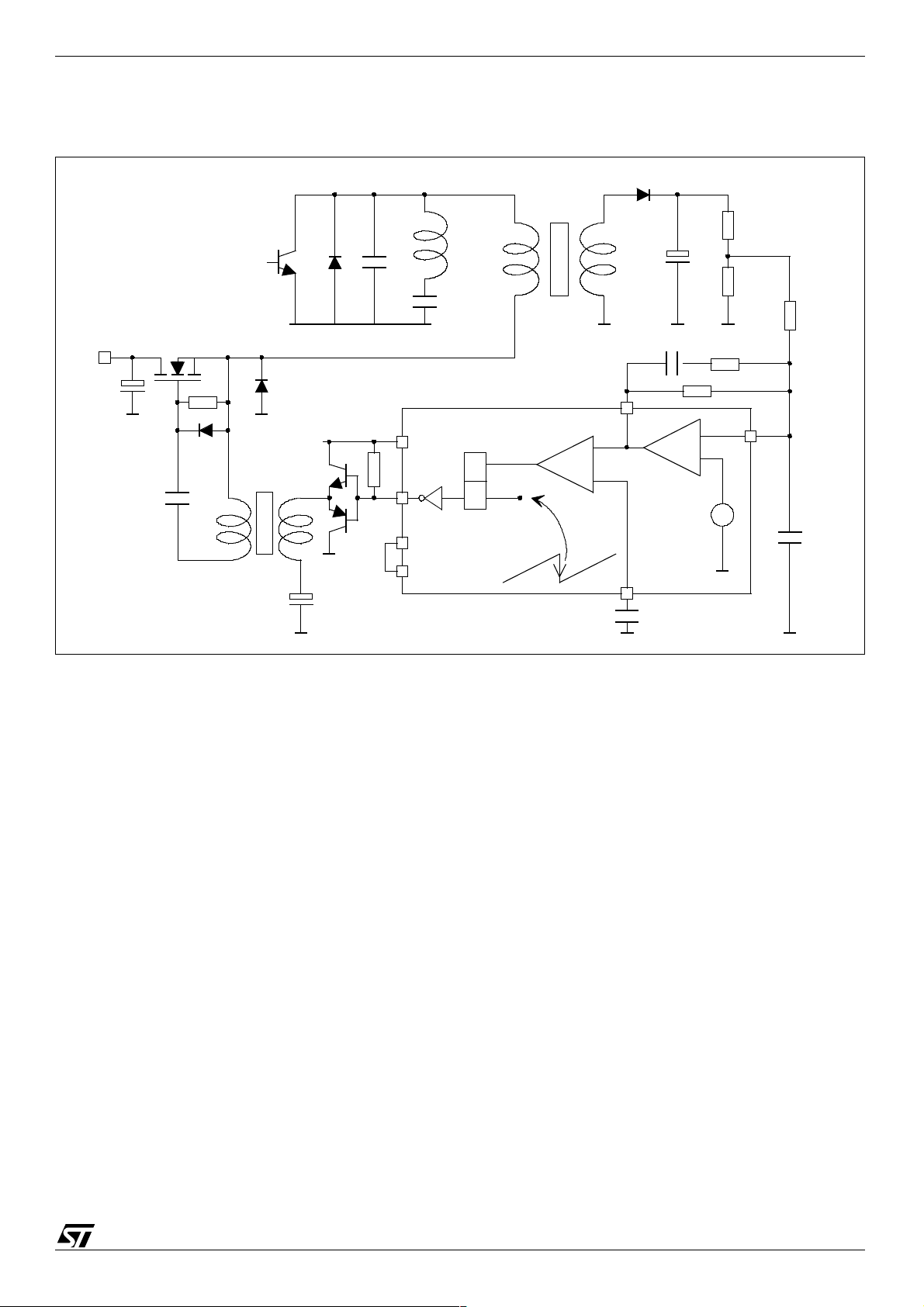
Obsolete Product(s) - Obsolete Product(s)
AN1290 DC/DC Converter Section
Figure 20: Regulation Loop in Step-down, Voltage Mode (MOS type N) (TDA9112 only)
Vdc
H scanning
transistor
TMOS Zfb:
29
28
13
16
Ly
T
Vb
14
Vo
Reset
Q
Set
+
-
H Focus
Capacitor
R1
Cr
R2
Ri
Cfb
9
Rfb
+
Vref
Rc
15
Vi
10nF
7.1.9 Structure of the DC/DC Converter (Open Loop)
A scanning stage needs a B+ roughly proportional to the frequency (Figure 21). An easy way to
provide this is by using a continuous conduction step-down converter; if conduction time is
maintained constant, the duty factor will be proportional to frequency. The same applies to the
output voltage.
Since there is no f eedback to cope with variab le beam current consumption, this archi tecture should
be reserved for monitors wit h separate EHV and scanning. Also, fine tuning should be made with
the HAmpl adjustment.
If the pulse duration is modulated by the E/W signal, the output voltage will be modulated
accordingly. The DC current sunk by the E/W pin from pin 15 ma y be compensated for with a pull-up
resistor to pin 15.
Minor changes from the TDA9111 DC/DC section make the TDA9112 able to provide a constantduration pulse, according t o Figure 21. A P-MOS high- side s witch has b een represented ( controlled
through capacitor). As usual, an N-MOS with transformer coupling could also be used, with some
adaptation of the monostabl e circuit. Since a flyback pulse is not required either for the EHV or for
voltage feedback purposes, L is directly connected to the S capacitor.
STMicroelectronics Confidential 49/62
Page 50

Obsolete Product(s) - Obsolete Product(s)
DC/DC Converter Section AN1290
Figure 21: DC/DC converter in Step-down, Open loop, MOS type p
Vdc
TMOS
Vb
Ly
29
28
16
Cfb
L
Reset
Q
Set
HOut
Zfb:
Rfb
14
Vo
+
Vref
E/W
Ri
Rc
Pull-up
+
15
Vi
The monostable circuit can be implemented with a capacitor charged from a constant supply
through a resistor. If the unregulated Vdc is used to feed the charge resistor, any ripple of Vdc,
which would normally entail an equivalent ripple on B+, will be automatically compensated by a
proportional variation of the conduction time (feed forward compensation). Discharge takes place
through a small FET when B+Out goes HIGH, swit ching OFF the power MOS transistor.
The pulse duration is set and modulated by the voltage on pin 14. Since there is no feedb ack, the
phase rotation due to the out put filt er has no h armful consequences and E/W ma y be applied to pin
15. Nev ertheless, the filter v al ue should be kept low, so as not to distort the output wavef orm on fast
transients.
7.2 Application Hints
7.2.1 Parasites induced by DC/DC Converter (Timing Selection)
When using the Step-down, Voltage mode configuration, there is no need to choose a timing, since
the current flow will automatically begin simultaneously with the HFoc us ramp, which is also used
for comparison with the op-amp output.
When using either Step-up or Step-down, current mode, at first glance, triggering after flyback
should be convenient. Nevertheless, you have to consider that switching OFF the power MOS
transistor will cause an intense parasitic voltage which may dist urb some other events. Although
there are techniques t o reduce the par asitic volt age and the IC s usceptibility, a more stra ightf orward
solution is to pre vent the switching from coinciding with any critical event.
The critical ev ents are the f ro nt edge of the HSync signa l, the edges of fl yback pulses (a ll located i n
the vicinity of FB pulse), the front edge of the HOut signal (fi rst half of H ramp) and the top and
bottom of sawtooth.
50/62 STMicroelectronics Confidential
Page 51
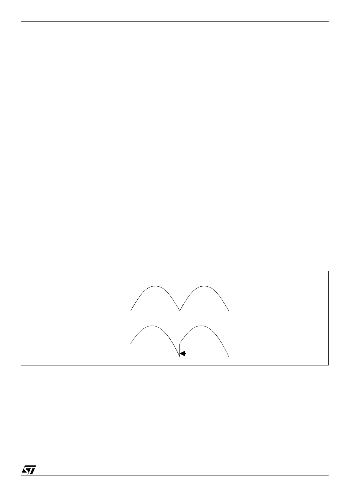
Obsolete Product(s) - Obsolete Product(s)
AN1290 DC/DC Converter Section
Considering that the BOut control pul se will ha ve constant duration (Open loop), or nearly constant
(Current mode, Step-up or Step-down), you can choose to trigger conduction:
● at low frequency, with HOut down,
● at high frequency, after flyback,
and obtain that the switching always ta k es pl ace inside the first half of H positi ve ramp, which is the
least critical period regarding parasitic voltage.
In Step-up, Current mode, any timing is convenient; nevertheless, usually disturbances will be
minimized when triggering with HOut up.
7.2.2 Frame-top Distortion related to Keystone Correction
This distortion mainly appears in monitors with separated EHV and scanning (though it can also
take place with diode modulators, in relation with the modulator amplifier).
In the monitors of this category, E/W correction is obtained by modulating the value of the B+
scanning stage with a parabolic waveform.
If there is no Keystone correction, the E/W waveform is continuous, and B+ scanning can easily
follow.
But as soon as Keystone correction is introduced there appears a fast transition (positive or
negative) between the end of a frame and the beginning of the next one as shown in Figure 22. To
get the B+ scanning to follow this wa veform, it would be necessary to charge or discharge at a very
high rate the Cb capacitor which proves difficult because the available current is limited.
Consequently, it is mandatory to maintain the Cb v alue as lo w as possi b le (possi bly less than 1µF).
A limiting fact or of course is the increasing B+ ripple at the horizontal frequency. Regarding this
aspect, the architectures that do not need Cb have a distinctive advantage (step-down, current
mode or open-loop).
Figure 22: E/W Waveforms
Without Keystone
With Keystone
Fast
Transition
Once Cb is made small enough to charge or discharge within the vertical blanking time , there may
remain a distortion of the frame top which corresponds to the transient response of the global
DC/DC feedbac k loop to t he fast transition. The res ponse may be damped or oscillatory depending
on horizontal frequency. Again, the transient phenomena should be finished within the vertical
blanking time. For that purpose, the loop response must be fast enough. Once Cb has been made
minimum the only possib le action is on t he frequency c ompensation of the op- amp between pins 14
and 15. A good starting value is given by Ri x Cfb = 15 µs. The op-amp itself has a unity gain of
6MHz and is not a limiting factor.
STMicroelectronics Confidential 51/62
Page 52

Obsolete Product(s) - Obsolete Product(s)
Miscellaneous AN1290
8 Miscellaneous
8.1 Summary of Safety Functions
Vertical, horizontal and B+ output stages will be inhibited (and for Vertical, voltage will be
maintained near mid-range, i.e. 3.5 / 8 of the reference voltage)
● when the supply voltage is too low;
● following a proper I²C instruction (Sad17h/d1 and Sad17h/d2).
Horizontal and B+ output stages will be inhibited if the X-ray protection threshold (8V on pin 25) is
exceeded. In such case, the H scanning and B+ are definitively stopped, and will only be reset by
switching the supply OFF or through I²C programming (Sad16h/d7). (Please notice that inhibition
affects only the output stages and not the oscillators. Consequently, I²C instructions will be still
transmitted during V Oscillator discharge).
In addition, the H output stage will be inhibi ted for the entire duration of H flyback, to prevent early
conduction of the scanning transistor.
Please refer to Figure 23 for a simplified logic diagram. The following are not represented here , b ut
are already described in this Note:
● Disable through X-ray pin will be activated only 2 lines after the threshold has been
exceeded, in order to prevent incorrect triggering on very shor t parasitic voltages;
● Soft-start will take place every time when switching ON or enabling again. H Duty factor will
always start with maximum value (85%), and progressively reach its assigned value
(consequently, conduction time will begin with minimum value). Similarly, B+Out will begin with
minimum conduction time and increase progressively towards its assigned value.
Figure 23: Safety Functions (Simplified)
I²C
Supply
Ref V
X-ray
I²C
Reset
Supply
Reset
H flyback
H drive OFF
H Output
Inhibition
sQ
r
B+ Output
Inhibition
0.7V
V Output
I²C
V ramp OFF
Inhibition
Miscellaneous functions a vailable on the TDA9112A only:
● X-ray detection is not triggerable if the supply voltage is lower than 10.4V, to prevent triggering
on a rapid ON-OFF-ON sequence while its filter maintains X-ray input at high voltage.
52/62 STMicroelectronics Confidential
Page 53

Obsolete Product(s) - Obsolete Product(s)
AN1290 Miscellaneous
● BMute function (1Fd6): B+ can be enabled/disabled alone, it will come back with its own soft-
start.
● BSafe function: i f it is selected throug h I²C (Sad1Fh/d5), BOut will s witch OFF as soon as the H
oscillator Unlock is de tected; when it locks again, B+ will come back wit h its own soft-start.
● HLock speed: If bit 1Fd2 is set , an Unloc k ed state wil l be detected t wice as f as t as with the r est
of the family. Remember that a mode with composite sync, long ver tical sync and no serration
pulses could unduly indicate Unloc k!
● Identification bit 1Fd3 allows to identify by software whether the IC is the TDA9112A or not.
8.2 Early V Blanking and Lock/Unlock
The TDA9112 family delivers an early blanking pulse on pin 3. The purpose is to provide early V
blanking (synchronous to VSync), because blanking from the V Flyback pulse alone would arrive
too late to blank the beginning of the retrace. The pulse begins with the VSync front edge, and
finishes with the end of the VCapacitor discharge. For correct V blanking, it needs to be ORed
with the VFlyback data.
The pulse amplitude is always 1V (enough to control a small bipolar transistor). It is superimposed
above the HLoc k/Unl oc k le v el (0 V when loc k ed, 5V when Unlock e d). If y ou conn ect the tr ansist or in
DC, blanking will be permanent when Unlocked. Refer to Application Hints if you want the display
(and OSD if any) to be visible also when Unlocked.
The Unlock indicat ion ma y be disab led t hrough I²C prog ramming ( Sad16h/d0). Permanent blanking
may be forced with 17d0.
8.3 Application Hints
8.3.1 Using Inhibition Properly
Emergency Procedure with H-Lock; V Blanking
Inhibition through I²C should be used with care for the following reason: When horizontal scanning
is inhibited, B+ is inhibited at the same time. Since scanning is stopped, there is no more power
consumption and B+ will keep its last value for possibly a fraction of a second. If inhibition
disappears at that moment, the horizontal frequency may have changed to a lower value. Starting
again in this condition is dangerous for the scanning transistor.
In a practical case, the i nhibition was triggered because some very high frequency H sync pulses
appeared when switching from high-frequency to low-frequency mode. These pulses were unduly
interp re te d a s “frequency out of range”.
Figure 24 shows an application diagram used to ensure a safe restart.
Further to the normal feedback resistive network which senses the horizontal amplitude, a second
one with lower impedance is directly connected to B+. Resistors are calculated to maintain B+ at a
low value, for instance low er than the free-running value. Ho wever, a diode and a transistor keep it
isolated from the normal resistive network as long as pin 3 remains LOW.
As soon as any change appears in the Hsync frequency, pin 3 goes HIGH, rapidly discharging the
3.3µF capacitor , and B+ decreases do wn to the v alue imposed b y the lo w-impedance netw ork. This
must be completed bef ore Inhibition takes place. When the H freq uency locks again, pin 3 goes
LOW again. The transi stor saturates again after a delay set by the 3.3µF capacitor to ensure that
Inhibition is finished. Then B+ will resume its normal value after a soft-start.
STMicroelectronics Confidential 53/62
Page 54

Obsolete Product(s) - Obsolete Product(s)
Miscellaneous AN1290
Figure 24: H Lock and V Early Blanking
H amp
TDA9112
feedback
3
0.1uF
Blank
22k
12V
220k
100k
3.3
uF
The resistor divider which cont rols t he base s hould take into account that a 1V bla nking si gnal may
be present even when Locked.
An AC-coupled transistor will provide an early negative-going blanking pulse (to be ORed with a
blanking pulse from V flyback). Still, because of the AC coupling, the display will be present when
Unlocked (important to display the OSD).
14
100
47k
15
B+
54/62 STMicroelectronics Confidential
Page 55

Obsolete Product(s) - Obsolete Product(s)
AN1290 I²C Con t r o l Se ction
9I²C Control Section
9.1 I²C Bus Reminder
Since I²C bus documentation is widespread today, a short reminder will be enough.
I²C bus consists of two wires , SCL (clock) and SDA (data), plus ground. The logic is positive. Bot h
SCL and SDA have a pull-up resistor to 5V, and all connected ports are open-collector or opendrain, i.e. a ct as wired AND (line is LOW if at least one port is LOW).
The ICs connected to the bus either belong to the MASTER or the SLAVE category:
● MASTERS control the clock and send/receive data
● SLAVES receive or send data when required by a MASTER, but do not control the clock.
All data is exchanged as 8-bit bytes (MSB first, LSB last), followed by an Acknowledge bit if a
SLAVE is the receiver. A logic 1 is recognized each time SDA remains HIGH for a full SCL pulse, a
logic 0 each time SD A remains LO W f or a full SCL pulse. I f a MASTER s witches SDA to LOW while
SCL is HIGH this is interpreted as START. The opposite tr ansition is interpreted as STOP. A SLAVE
receiver will acknowledge receipt of the data by maintaining SDA LOW for the full duration of the
next clock pulse, while the MASTER transmitter leaves SDA floating.
9.2 TDA9112 Family as I²C Bus Device
For a complete overview of I²C programming values, refer to Section 10: I²C Bus Control Register
Map on page 60
In the TDA9112 family, all settings are programmed through the I²C bus. All ICs in the family are
software-compatible, including the TDA9112A which uses more instructions. Clock frequency may
be as high as 400 kHz. The duration of any pulse must be higher than 50ns, because parasitic
spikes are filtered with this time constant. The input threshold for receiving data on pins 31 (SDA)
and 30 (SCL) is 2.2 V typ when the supply on pin 32 is 5 V. Logic levels are TTL compatible when
sending data.
The logic section is biased by an internal 5 V supply. At start-up, all internal registers stay reset to
their default value until the supply volt age exceeds 8.5 V, they are reset again when it goes lower
than 6.5 V (8.0 V and 6.8 V for TDA 9112A).
The TDA9112 family is SLAVE only. Like all I²C devices it has an 8 bit-address which is
(hexadecimal) 8C when receiving and 8D when sending data (the TDA9115 does not send data).
To know the affectation of the various registers, please refer to the register map.
9.3 Receiving Data
The data for the v arious controls are st ored in 24 ⋅ (8-bit regist ers) with thei r 24 sub addresses on 8
bits (31 registers f or the TD A9112A). Since not more than the 5 or 6 LSB are necessary to define 24
or 31 sub addresses, the 3 or 2 MSB are undefined.
Nevertheless, f o r the sake of compatibility with future softw are it is recommended to set them to 0.
The same applies to all unspecified bits.
When the microprocessor sends one piece of data to one register, the following sequence will
appear on the bus: (Codes sent b y the TDA9112 in Bold)
(Start)(8C)(ackn)(subadress)(ackn)(data)(ackn)(Stop)
STMicroelectronics Confidential 55/62
Page 56

Obsolete Product(s) - Obsolete Product(s)
I²C Control Section AN1290
In order to make the transmission of long strings of data easier, the TDA9112 features an autoincrement function. This means that the sub address will increase by one after receiving each byte
of data. This is especially useful when initializing all registers at start-up. The corresponding
sequence on the bus would be as follows:
(Start)(8C)(ackn)(00)(ackn)(data00)(ackn)(data01)(ackn)...(data0F)(ackn)(Stop)
Some peculiarities of the various registers wil l be summarized later.
9.4 Sending Data
When required by the microprocessor, the TDA9112 will send the contents of its unique read-mode
register as data, which summarize its status (in the family, only the TDA9115 does not have a readmode register and will not send data).
This register is a latch, consequently it mus t be updated to mak e sur e that its cont ent is recen t and
valid:
(Start)(8C)
It is not necessary to reset the Refresh bit (it will go bac k to 0 by itself).
Then the TDA9112 can be requested to send its data. Since there is only one register , no sub
address is necessary:
9.5 Register Organization
The values in Bold are default v a lues, forced during initial Reset. Of course, it is up to the user to
load different values when starting, for instance with the help of the Auto-increment feature
explained above. Nevertheless, the default values will always appear first.
Synchronization to Vertical
The register contents sent to the TDA9112 are first latched; the y will be transferred only during the
retrace of ve rtical oscillator. This way, the display is never modified in the visible part of the frame.
This is not true for enable/disable bits which are always immediately transferred (most d7 plus all
Add 16, 17, 1F). These bits are toggles, except 16 d4 and d7 (reset bits) which will return to 0 by
themselves.
(ackn)(16)(ackn)(xxx1xxxx)(ackn)(Stop)
(Start)(8D)
(ackn)(data)(Stop)
Warning! If there is no oscillator retrace, no setting will be transmitted! This may happen if the
Vertical section is not wired, but disabling VOut does not impair transmission.
Table 3: Detailed Register Description (including TDA9112A) (Sheet 1 of 3)
Reg. Add. Comments
00d7 1: HDuty value is transferred with next VOscillator discharge.
01d0 d0 is only significant in the TDA9112 and the TDA9112A, granting them 8-bit H position adjustment while
02d7 1: Moire cancellation is suited to Separate scanning and EHV.
03d7 1/0: same behavior as 00d7, for B+ value.
56/62 STMicroelectronics Confidential
0: HDuty value is immediately transferred
maintaining software compatibility with the 7 bits of the TDA9112, TDA9113, TDA9115 and TDA9116.
0: Moire cancellation is suited to Combined structure.
Page 57

Obsolete Product(s) - Obsolete Product(s)
AN1290 I²C Con t r o l Se ction
Table 3: Detailed Register Description (including TDA9112A) (Sheet 2 of 3)
Reg. Add. Comments
04d7 1: Hfocus amplitude will track Hamplitude / 0: no tracking.
05d7 1: The HFocus signal will start at middle of flyback;
0: - at beginning of flyback.
Signal begins with a flat corresponding to internal capacitor discharge; Internal ramp, and parabola, begin just
after.
Same timing for th e DC/DC co nv erter current if the Step-down, Voltage mode configuration is us ed (More tha n 6V
on pin 16; TDA9112 only).
06d7 If 1: BOut will go to LOW level to make the power MOS conductive (adapted to type P) / if 0, adapted to type N
07d7 1: DC/DC converter current will start.with either HOut UP or HOut DOWN (which one, depends on 17d3)
0: DC/DC converter current will start just after flyback (see 17d3 for the TDA9112A special).
9112 only: This bit has n o effect when pin 16 is biased over 6V for Step-down, Voltage mode.
08d7 1: all corrections available on E/W output will keep proportional to H frequency, i.e. to the voltage on pin 9 (till it
reaches 5V).
0: all corrections available on E/W output will keep the value corresponding to 5V
10d0 d0 is only significant in the TDA9112 and the TDA9112A, granting them 8-bit H amplitude adjustment while
maintaining software compatibility with the 7 bits of the TDA9112, TDA9113, TDA9115 and TDA9116.
15d7 0: the VFocus parabola on pin 32 will present an upward concavity ∪.
1: this VFocus parabola will present a downward concavity ∩
16d0 1: HLock/Unlock indication will be available on pin 3, added to VBlanking.
0: VBlanking alone.
16d1 1: PLL1 will be inhibited for the duration of extracted VSync (necessary if serration pulses are absent)
0: PLL1 will not be inhibited.
16d2 1: charge pump current will be 1mA
0: charge pump current will be 0.3mA.
16d3 (TDA9112A only) 0: minimum charge pump current (total 4steps with 16d2,d3)
(TDA9116 only) 0: HMoire applied internally, pin 11 is a DAC.set by (02) /1: HMoire waveform on pin 11
16d4 1: If a 1 is sent, the Read mode register will be refreshed (mandatory before reading).
After reading, this bit will return to 0 by itself (no Reset needed).
16d5, d6 If d6 is 1, the IC will select and keep the first arrived VSync (be it Separate or Composite)
If d6 is 0, the IC will use the VSync indicated by d5 as follows:
- if d5 is 1, separate sync will be selected
- if d5 is 0, whatev er VSync th at ma y be ex tracted on H input (if noth ing can be e xtrac ted, v ertical frequen cy will go
to free-run)
16d7 Sending a 1 will reset X-ray protection / return to 0 is automatic)
17d0 1: the Blanking HIGH level (1V, possibly added to HLock level) will be permanent
17d1, d2 1: Enabled /0: disabled VOut and H/BOut respectively.
0: normal blanking operation.
Sending a 1 to 17d2 triggers Soft-Start for HOut and BOut.
A Disable instruction may come als o from other sections (see Safety functions)
STMicroelectronics Confidential 57/62
Page 58

Obsolete Product(s) - Obsolete Product(s)
I²C Control Section AN1290
Table 3: Detailed Register Description (including TDA9112A) (Sheet 3 of 3)
Reg. Add. Comments
17d3 Active only if 07d7 is set to 1, except the TDA9112A.
1: sets the triggering of B+ to HDrive UP/0: sets to HDrive DOWN.
TDA9112A only: when 07d7 is 1, same as previous/when 07d7 is 0:
if 17d3 is 0, same as previous (triggers after flyback)
if 17d3 is 1, triggers with top of sawtooth, at half H frequency.
17d4,d5,
d6, d7
1: These bits are set to 1 only while testing the IC in factory. Users must keep them bound to 0.
T able 4: Extra Registers (TDA9112A Only)
Reg. Add. Comments
1Fd0 0: The flat in HDyCor waveform begins at initial point of HDyCor signal (see 05d7)
1: anticipated at the beginning of H flyback
1Fd1 0: HVDyCor concavity (of both H and V parabolas) upwards ∪
1: concavity downwards ∩
1Fd2 0: Delay for detecting H Unlock, same as the TDA9112 family
1: Delay divided by 2
1Fd3 When 17d2 HBOutEn is 0 (disabled):
0: HLock bit (d7 of Read register) is 1 (similar to the TDA9112 family)
1: HLock bit is 0 regardless of lock status
When HBOutEn is 1, HLock bit monitors lock ing (0 if locked)
1Fd4 0: All corrections on E/W pin, including DC for HSize setting, track the H frequency
1: No tracking
1Fd5 0: BSafe disabled
1: BSafe enabled: B+ will stop as soon as HUnlock id detected
1Fd6 0: B+ can operate if otherwise allowed
1: B+ disabled
A soft-start takes place whenever B+ resumes operation in relation with 1Fd5 or 1Fd6
1Fd7 Threshold on pin 16 which stops B+ conduction
0: 2.1V (same as the TDA9112 family; suitable to build an RC ramp generator)
1: 1.2V (more convenient for ISense)
Note: Bold denotes values at Power-on reset.
58/62 STMicroelectronics Confidential
Page 59

Obsolete Product(s) - Obsolete Product(s)
AN1290 I²C Con t r o l Se ction
9.6 Management of Status Register and Sync Priority
It is possible to read from the STATUS register (Bold = default value):
● in d0, whether pulses are present on pin 2 Vsync (1 = detected once/0 = not detected yet)
● in d1, whether pulses are present on pin 1 H/HVsync (1 = detected once/0 = not detected yet)
● in d2, whether a Vsync can be e xt rac ted f rom H/HV s ignal ( 1 = d etected onc e/0 = not detec ted
yet)
● in d4-d3, the signs of t hose sync pulses which have been selected with 16d6, d5 (1 = negative
or not detected/0 = positive)
● in d5, the status of X-ray alarm (1 for Alarm ON, Hout inhibited/0 = Alarm OFF))
● in d7d6, the Lock/Unlock status of H and V oscillators (1 = Unlocked/0 = Locked)
Warning! A d0,d1 or d2 at 1 just means that at least one sync pulse arrived since last SDetReset.
For obvi ous reasons, Reset cannot be automatic, therefore, all Sync data must be obtained as
follows:
● Reset detection bit
● Wait for longer than the maximum expected period
● Read detection bit
Combining this data, the microproce ssor has to sel ect (by setting bits 16d5, 6) which sync data will
effectively trigger the H and V oscillators.
STMicroelectronics Confidential 59/62
Page 60

Obsolete Product(s) - Obsolete Product(s)
I²C Bus Control Register Map AN1290
10 I²C Bus Control Register Map
The device slave address is 8C in write mode and 8D in read mode. The control register map is
given in Table 5. The values in bold denote the default v alue at Power-On-Reset.
I²C-bus data in the adjustment register is buffered and internally applied with discharge of the
vertical oscillator (). In order to ensure compatibility with future devices, all “Reserved” bits should
be set to 0.
Table 5: I²C-bus Control Registers
SadD7D6D5D4D3D2D1D0
Write Mode (Slave Address = 8C)
00 HDutySyncV
1: Synchro.
0: Asynchro.
01 HPOS Horizontal Position
10000000
02 HMoiréMode
1: Separated
0: Combined
03 B+SyncV
0: Asynchro.
04 HDyCorTr
0: Not active
05 HDyCorPh
1: Middle
0: Start
06 BOutPol
0: Type N
07 BOutPh
0: H-flyback
1: H-drive
08 EWTrHFr
0: No tracking
09 Reserved
0A Reserved
0B Reserved
0C Reserved
0D Reserved
0E Reserved
0F Reserved
0 0 0 0 0 0 0
0000000
1000000
1000000
1000000
1000000
1000000
1000000
1000000
1000000
0000000
1000000
1000000
1000000
1000000
HDUTY Horizontal Duty Cycle
HMOIRE Horizontal Moiré Amplitude
BREF B+reference
HVDC-HAMP HVDyCor horizontal amplitude
HVDC-HPH HVDyCor horizontal phase
HVDC-VAMP HVDyCor vertical amplitude
VSIZE Vertical Size
VPOS Vertical Position
SCOR S-correction
CCOR C-correction
VMOIRE Vertical Moiré Amplitude
PCC Pin Cushion Correction
KEYST Keystone Correction
TCC Top Corner Correction
BCC Bottom Corner Correction
60/62 STMicroelectronics Confidential
Page 61

Obsolete Product(s) - Obsolete Product(s)
AN1290 I²C Bus Control Register Map
Table 5: I²C-bus Control Registers
SadD7D6D5D4D3D2D1D0
10 HSIZE Horizontal Size
10000000
11 Reserved
1000000
12 Reserved
1000000
13 Reserved
1000000
14 Reserved
1000000
15 VDyCorPol
0:”∪“
16 XRayReset
0: No effect
1: Reset
17 TV
18 Reserved
19 Reserved
1A Reserved
1B Reserved
1C Reserved
1D Reserved
1E Reserved
1F ThrBlsense
Read Mode (Slave Address = 8D)
()
XX
1: Not locked
()
0: Off
0:
0:
0:
0:
0:
0:
0:
0: High
HLock
0: Locked
1000000
VSyncAuto
1: On
TH
()
0: Off
0000000
1000000
1000000
0000000
0000000
1110000
1000000
BMute
0: Off
VLock
0: Locked
1: Not lock.
PCAC Pin Cushion Asymmetry Correction
PARAL Parallelogram Correction
TCAC Top Corner Asymmetry Correction
BCAC Bottom Corner Asymmetry Correction
VDC-AMP Verti cal Dy namic Correction
VSyncSel
0:Comp
1:Sep
TVM
()
0: Off
HVDC-HSHAP HVDyCor Horizontal Shape
EWSC East-West S-correction
EWWC East-West W-correction
HEHTG Horizontal EHT Compensation Gain
VEHTG Vertical EHT Compensation Gain
VSAG Vertical Size After-gain
VPOF V ertical Position Offset
BSafeEn
0: Disable
XRayAlarm
1: On
0: Off
SDetReset
0: No effect
1: Reset
THM
()
0: Off
EWTrHSize
0: Tracking
PolarityDetection Sync Detection
HVPol
1: Negative
0: No effect
1: Negative
PLL1Pump
1,1: Fastest
0,0: Slowest
BOHEdge
0: Falling
Ident
VPol
HBOutEn
0: Disable
HLockSpeed
0: Slow
VExtrDet
0: Not det.
PLL1InhEn
VOutEn
0: Disable
HVDyCorPol
0: Not det.
1: On
0:”∪“
HVDet
HLockEn
1: On
BlankMode
1: Perm.
HDCFlatEn
0: Disable
VDet
0: Not det.
Note: 1 With exception of HDUTY and BREF adjustments data that can take effect instantaneously if
switches HDutySyncV and B+SyncV are at 0, respectively.
2 In Read Mode, the device always outputs data of the status register, regar dless of the subaddress
previously selected.
3 The TV, TH, TVM and THM bits are for testing purposes and must be kept at 0 by application.
STMicroelectronics Confidential 61/62
Page 62

Obsolete Product(s) - Obsolete Product(s)
I²C Bus Control Register Map AN1290
Notes:
Information furnished is believed to be accurate and reliable. However, STMicroelectronics assumes no responsibility for the
consequences of use of such information nor for a ny in fring em en t of patents or other rights of third parties which may result f rom its
use. No license is granted by implication or otherwise under any patent or patent rights of STMicroelectronics. Specifications
mentioned in this pub lication are subjec t to change without notic e. This publication supersedes and replace s all information pr eviously
supplied. STMicroelectronics products are not authorized for use as critical components in life support devices or systems without
express written approval of STMicroelectronics.
The ST logo is a registered trademark of STMicroelectronics
Australia - Brazil - Canada - China - Finland - France - Germany - Hong Kong - India - Israel - Italy - Japan
Malaysia - Malta - Morocco - Singapore - Spain - Sweden - Switzerland - United Kingdom - U.S.A.
62/62 STMicroelectronics Confidential
© 2002 STMicroelectronics - All Rights Reserved
STMicroelectronics GROUP OF COMPANIES
www.st.com
 Loading...