

Page 1
Features
■ Input multiplexer
– Multiple input configuration for different
application
■ Loudness
–2
– Programmable center frequency
– 15 dB with 1 dB steps
– Selectable high frequency boost
– Selectable flat-mode
■ Volume
– +15 dB to -15 dB with 1 dB step resolution
– Soft-step control with programmable blend
times
■ Bass
–2
– Center frequency programmable in 4 steps
– Q programmable 1.0/1.25/1.5/2.0
– DC gain programmable
– -15 to 15 dB range with 1 dB resolution
■ Middle
–2
– Center frequency programmable in 4 steps
– Q programmable 0.5/0.75/1.0/1.25
– -15 to 15dB range with 1dB resolution
■ Treble
–2
– Center frequency programmable in 4 steps
– -15 to 15dB range with 1dB resolution
■ Speaker
– 4 independent soft step speaker controls
– 0dB to -79dB with 1dB steps
–Direct mute
■ Subwoofer
–2
cut off frequency
– 2 independent soft step level control,
■ Mute functions
nd
order frequency response
nd
order frequency response
nd
order frequency response
nd
order frequency response
nd
order low pass filter with programmable
TDA7719
3 band car audio processor
TSSOP28
– Direct mute
– Digitally controlled SoftMute with 4
programmable mute-times
■ Offset detection
– Offset voltage detection circuit for on-board
power amplifier failure diagnosis
■ Level meter
– Provide rectified level voltage of main
source signal (before loudness)
■ Rear seat selector
– Full source selector for rear seat output
■ Mixing selector
Description
The TDA7719 is a high performance signal
processor specifically designed for car radio
applications. The device includes a high
performance audioprocessor with fully integrated
audio filters and new Soft Step architecture. The
digital control allows programming in a wide range
of filter characteristics. By the use of BCMOSprocess and liner signal processing low distortion
and low noise are obtained.
Table 1. Device summary
Order code Package Packing
TDA7719 TSSOP28 Tube
TDA7719TR TSSOP28 Tape and reel
April 2009 Doc ID 13698 Rev 4 1/46
www.st.com
1
Page 2

Contents TDA7719
Contents
1 Block circuit diagram . . . . . . . . . . . . . . . . . . . . . . . . . . . . . . . . . . . . . . . . 6
2 Pin description . . . . . . . . . . . . . . . . . . . . . . . . . . . . . . . . . . . . . . . . . . . . . 7
2.1 Pin connection . . . . . . . . . . . . . . . . . . . . . . . . . . . . . . . . . . . . . . . . . . . . . . 7
2.2 Pin description . . . . . . . . . . . . . . . . . . . . . . . . . . . . . . . . . . . . . . . . . . . . . . 7
3 Electrical specifications . . . . . . . . . . . . . . . . . . . . . . . . . . . . . . . . . . . . . . 9
3.1 Thermal data . . . . . . . . . . . . . . . . . . . . . . . . . . . . . . . . . . . . . . . . . . . . . . . 9
3.2 Absolute maximum ratings . . . . . . . . . . . . . . . . . . . . . . . . . . . . . . . . . . . . . 9
3.3 Electrical characteristics . . . . . . . . . . . . . . . . . . . . . . . . . . . . . . . . . . . . . . . 9
4 Description . . . . . . . . . . . . . . . . . . . . . . . . . . . . . . . . . . . . . . . . . . . . . . . . 13
4.1 Input configuration . . . . . . . . . . . . . . . . . . . . . . . . . . . . . . . . . . . . . . . . . . 13
4.1.1 Front and rear selector . . . . . . . . . . . . . . . . . . . . . . . . . . . . . . . . . . . . . . 13
4.1.2 Direct path . . . . . . . . . . . . . . . . . . . . . . . . . . . . . . . . . . . . . . . . . . . . . . . 15
4.2 Mixing . . . . . . . . . . . . . . . . . . . . . . . . . . . . . . . . . . . . . . . . . . . . . . . . . . . . 16
4.3 Loudness . . . . . . . . . . . . . . . . . . . . . . . . . . . . . . . . . . . . . . . . . . . . . . . . . 17
4.3.1 Loudness attenuation . . . . . . . . . . . . . . . . . . . . . . . . . . . . . . . . . . . . . . 17
4.3.2 Peak frequency . . . . . . . . . . . . . . . . . . . . . . . . . . . . . . . . . . . . . . . . . . . 17
4.3.3 High frequency boost . . . . . . . . . . . . . . . . . . . . . . . . . . . . . . . . . . . . . . . 18
4.3.4 Flat mode . . . . . . . . . . . . . . . . . . . . . . . . . . . . . . . . . . . . . . . . . . . . . . . . 18
4.4 SoftMute . . . . . . . . . . . . . . . . . . . . . . . . . . . . . . . . . . . . . . . . . . . . . . . . . . 18
4.5 Softstep volume . . . . . . . . . . . . . . . . . . . . . . . . . . . . . . . . . . . . . . . . . . . . 19
4.6 Bass . . . . . . . . . . . . . . . . . . . . . . . . . . . . . . . . . . . . . . . . . . . . . . . . . . . . . 19
4.6.1 Bass attenuation . . . . . . . . . . . . . . . . . . . . . . . . . . . . . . . . . . . . . . . . . . 19
4.6.2 Bass center frequency . . . . . . . . . . . . . . . . . . . . . . . . . . . . . . . . . . . . . . 19
4.6.3 Bass quality factors . . . . . . . . . . . . . . . . . . . . . . . . . . . . . . . . . . . . . . . . 20
4.6.4 DC mode . . . . . . . . . . . . . . . . . . . . . . . . . . . . . . . . . . . . . . . . . . . . . . . . 20
4.7 Middle . . . . . . . . . . . . . . . . . . . . . . . . . . . . . . . . . . . . . . . . . . . . . . . . . . . . 21
4.7.1 Middle attenuation . . . . . . . . . . . . . . . . . . . . . . . . . . . . . . . . . . . . . . . . . 21
4.7.2 Middle center frequency . . . . . . . . . . . . . . . . . . . . . . . . . . . . . . . . . . . . 21
4.7.3 Middle quality factors . . . . . . . . . . . . . . . . . . . . . . . . . . . . . . . . . . . . . . . 22
4.8 Treble . . . . . . . . . . . . . . . . . . . . . . . . . . . . . . . . . . . . . . . . . . . . . . . . . . . . 22
2/46 Doc ID 13698 Rev 4
Page 3

TDA7719 Contents
4.8.1 Treble attenuation . . . . . . . . . . . . . . . . . . . . . . . . . . . . . . . . . . . . . . . . . 22
4.8.2 Treble center frequency . . . . . . . . . . . . . . . . . . . . . . . . . . . . . . . . . . . . . 23
4.9 Subwoofer Filter . . . . . . . . . . . . . . . . . . . . . . . . . . . . . . . . . . . . . . . . . . . . 23
4.10 Softstep control . . . . . . . . . . . . . . . . . . . . . . . . . . . . . . . . . . . . . . . . . . . . 24
4.11 DC offset detector and level meter option . . . . . . . . . . . . . . . . . . . . . . . . 25
4.12 DC offset detector . . . . . . . . . . . . . . . . . . . . . . . . . . . . . . . . . . . . . . . . . . 25
4.13 Level meter . . . . . . . . . . . . . . . . . . . . . . . . . . . . . . . . . . . . . . . . . . . . . . . . 26
4.14 Output gain control . . . . . . . . . . . . . . . . . . . . . . . . . . . . . . . . . . . . . . . . . . 26
4.15 Audioprocessor testing . . . . . . . . . . . . . . . . . . . . . . . . . . . . . . . . . . . . . . . 26
4.16 Test circuit (3 x QD + 1 x FD + DC offset detector) . . . . . . . . . . . . . . . . . 27
5I
2
C bus specification . . . . . . . . . . . . . . . . . . . . . . . . . . . . . . . . . . . . . . . . 28
5.1 Interface protocol . . . . . . . . . . . . . . . . . . . . . . . . . . . . . . . . . . . . . . . . . . . 28
5.1.1 Receive mode . . . . . . . . . . . . . . . . . . . . . . . . . . . . . . . . . . . . . . . . . . . . 29
5.1.2 Transmission mode . . . . . . . . . . . . . . . . . . . . . . . . . . . . . . . . . . . . . . . . 29
5.1.3 Reset condition . . . . . . . . . . . . . . . . . . . . . . . . . . . . . . . . . . . . . . . . . . . 29
5.2 Data byte specification . . . . . . . . . . . . . . . . . . . . . . . . . . . . . . . . . . . . . . . 31
6 Package information . . . . . . . . . . . . . . . . . . . . . . . . . . . . . . . . . . . . . . . . 44
7 Revision history . . . . . . . . . . . . . . . . . . . . . . . . . . . . . . . . . . . . . . . . . . . 45
Doc ID 13698 Rev 4 3/46
Page 4

List of tables TDA7719
List of tables
Table 1. Device summary . . . . . . . . . . . . . . . . . . . . . . . . . . . . . . . . . . . . . . . . . . . . . . . . . . . . . . . . . . 1
Table 2. Pin description . . . . . . . . . . . . . . . . . . . . . . . . . . . . . . . . . . . . . . . . . . . . . . . . . . . . . . . . . . . 7
Table 3. Thermal data. . . . . . . . . . . . . . . . . . . . . . . . . . . . . . . . . . . . . . . . . . . . . . . . . . . . . . . . . . . . . 9
Table 4. Absolute maximum ratings . . . . . . . . . . . . . . . . . . . . . . . . . . . . . . . . . . . . . . . . . . . . . . . . . . 9
Table 5. Electrical characteristics . . . . . . . . . . . . . . . . . . . . . . . . . . . . . . . . . . . . . . . . . . . . . . . . . . . . 9
Table 6. Input pin configuration . . . . . . . . . . . . . . . . . . . . . . . . . . . . . . . . . . . . . . . . . . . . . . . . . . . . 13
Table 7. Selector configuration matrix . . . . . . . . . . . . . . . . . . . . . . . . . . . . . . . . . . . . . . . . . . . . . . . 14
Table 8. Available sources for mixing . . . . . . . . . . . . . . . . . . . . . . . . . . . . . . . . . . . . . . . . . . . . . . . . 16
Table 9. I
Table 10. Subaddress (receive mode) . . . . . . . . . . . . . . . . . . . . . . . . . . . . . . . . . . . . . . . . . . . . . . . . 30
Table 11. Input configuration / main selector (0) . . . . . . . . . . . . . . . . . . . . . . . . . . . . . . . . . . . . . . . . 31
Table 12. 2nd Source selector / direct path (1). . . . . . . . . . . . . . . . . . . . . . . . . . . . . . . . . . . . . . . . . . 32
Table 13. Mixing source / mixing gain (2) . . . . . . . . . . . . . . . . . . . . . . . . . . . . . . . . . . . . . . . . . . . . . . 33
Table 14. Mix control / level meter / dc offset detector configure (3) . . . . . . . . . . . . . . . . . . . . . . . . . 34
Table 15. Soft mute / others (4) . . . . . . . . . . . . . . . . . . . . . . . . . . . . . . . . . . . . . . . . . . . . . . . . . . . . . 35
Table 16. SoftStep I (5). . . . . . . . . . . . . . . . . . . . . . . . . . . . . . . . . . . . . . . . . . . . . . . . . . . . . . . . . . . . 36
Table 17. SoftStep II / DC detector (6) . . . . . . . . . . . . . . . . . . . . . . . . . . . . . . . . . . . . . . . . . . . . . . . . 37
Table 18. Loudness (7) . . . . . . . . . . . . . . . . . . . . . . . . . . . . . . . . . . . . . . . . . . . . . . . . . . . . . . . . . . . . 38
Table 19. Volume / output gain (8) . . . . . . . . . . . . . . . . . . . . . . . . . . . . . . . . . . . . . . . . . . . . . . . . . . . 38
Table 20. Treble filter (9) . . . . . . . . . . . . . . . . . . . . . . . . . . . . . . . . . . . . . . . . . . . . . . . . . . . . . . . . . . 39
Table 21. Middle filter (10) . . . . . . . . . . . . . . . . . . . . . . . . . . . . . . . . . . . . . . . . . . . . . . . . . . . . . . . . . 39
Table 22. Bass filter (11). . . . . . . . . . . . . . . . . . . . . . . . . . . . . . . . . . . . . . . . . . . . . . . . . . . . . . . . . . . 40
Table 23. Subwoofer / middle / bass (12) . . . . . . . . . . . . . . . . . . . . . . . . . . . . . . . . . . . . . . . . . . . . . . 40
Table 24. Speaker attenuation (LF/RF/LR/RR) (13-16) . . . . . . . . . . . . . . . . . . . . . . . . . . . . . . . . . . . 41
Table 25. Subwoofer attenuation (subwoofer L/subwoofer R) (17-18) . . . . . . . . . . . . . . . . . . . . . . . . 41
Table 26. Testing audio processor 1 (19) . . . . . . . . . . . . . . . . . . . . . . . . . . . . . . . . . . . . . . . . . . . . . . 42
Table 27. Testing audio processor 2 (20) . . . . . . . . . . . . . . . . . . . . . . . . . . . . . . . . . . . . . . . . . . . . . . 43
Table 28. Document revision history . . . . . . . . . . . . . . . . . . . . . . . . . . . . . . . . . . . . . . . . . . . . . . . . . 45
2
C bus electrical characterisitics . . . . . . . . . . . . . . . . . . . . . . . . . . . . . . . . . . . . . . . . . . . . 28
4/46 Doc ID 13698 Rev 4
Page 5

TDA7719 List of figures
List of figures
Figure 1. Block circuit diagram. . . . . . . . . . . . . . . . . . . . . . . . . . . . . . . . . . . . . . . . . . . . . . . . . . . . . . . 6
Figure 2. Pin connection (top view) . . . . . . . . . . . . . . . . . . . . . . . . . . . . . . . . . . . . . . . . . . . . . . . . . . . 7
Figure 3. QD and FD configuration of QD4/FD4 . . . . . . . . . . . . . . . . . . . . . . . . . . . . . . . . . . . . . . . . 15
Figure 4. Block diagram of mixing stage . . . . . . . . . . . . . . . . . . . . . . . . . . . . . . . . . . . . . . . . . . . . . . 16
Figure 5. Loudness attenuation @ fP = 400 Hz. . . . . . . . . . . . . . . . . . . . . . . . . . . . . . . . . . . . . . . . . 17
Figure 6. Loudness center frequencies @ Attn. = 15 dB. . . . . . . . . . . . . . . . . . . . . . . . . . . . . . . . . . 17
Figure 7. Loudness attenuation, f
Figure 8. SoftMute timing . . . . . . . . . . . . . . . . . . . . . . . . . . . . . . . . . . . . . . . . . . . . . . . . . . . . . . . . . . 18
Figure 9. Bass Control @ fc = 80 Hz, Q = 1 . . . . . . . . . . . . . . . . . . . . . . . . . . . . . . . . . . . . . . . . . . . 19
Figure 10. Bass center frequencies @ gain = 14 dB, Q = 1 . . . . . . . . . . . . . . . . . . . . . . . . . . . . . . . . 19
Figure 11. Bass quality factors @ gain = 14 dB, f
Figure 12. Bass normal and DC mode @ Gain = 14 dB, f
Figure 13. Middle control @ fc = 1 kHz, Q = 1. . . . . . . . . . . . . . . . . . . . . . . . . . . . . . . . . . . . . . . . . . . 21
Figure 14. Middle center frequencies @ gain = 14d B, Q = 1 . . . . . . . . . . . . . . . . . . . . . . . . . . . . . . . 21
Figure 15. Middle quality factors @ gain = 14 dB, f
Figure 16. Treble Control @ fc = 17.5 kHz. . . . . . . . . . . . . . . . . . . . . . . . . . . . . . . . . . . . . . . . . . . . . . 22
Figure 17. Treble center frequencies @ gain = 14 dB . . . . . . . . . . . . . . . . . . . . . . . . . . . . . . . . . . . . . 23
Figure 18. Subwoofer control . . . . . . . . . . . . . . . . . . . . . . . . . . . . . . . . . . . . . . . . . . . . . . . . . . . . . . . . 23
Figure 19. DC offset detection circuit (simplified) . . . . . . . . . . . . . . . . . . . . . . . . . . . . . . . . . . . . . . . . 26
Figure 20. Test circuit . . . . . . . . . . . . . . . . . . . . . . . . . . . . . . . . . . . . . . . . . . . . . . . . . . . . . . . . . . . . . 27
Figure 21. Switching characteristics . . . . . . . . . . . . . . . . . . . . . . . . . . . . . . . . . . . . . . . . . . . . . . . . . . 28
Figure 22. I
2
C timing diagram . . . . . . . . . . . . . . . . . . . . . . . . . . . . . . . . . . . . . . . . . . . . . . . . . . . . . . . 29
Figure 23. TSSOP28 mechanical data and package dimensions . . . . . . . . . . . . . . . . . . . . . . . . . . . . 44
=2.4 kHz . . . . . . . . . . . . . . . . . . . . . . . . . . . . . . . . . . . . . . . . . . . 18
c
= 80 Hz. . . . . . . . . . . . . . . . . . . . . . . . . . . . . . . . . 20
c
c
= 80 Hz . . . . . . . . . . . . . . . . . . . . . . . . . . 20
c
= 1 kHz . . . . . . . . . . . . . . . . . . . . . . . . . . . . . . . 22
Doc ID 13698 Rev 4 5/46
Page 6
Block circuit diagram TDA7719
1 Block circuit diagram
Figure 1. Block circuit diagram
OUTL F
OUTRF
OUTLR
Mix
Mix
Mix
Mono Fader
Mono Fader
Mono Fader
OUTL2
OUTRR
Mix
Mono Fader
Subw oofer
OUTR2
LMOUT
Det ect o r
DC-Offset
Mono Fader
Mono Fader
Level Meter / Beep
LPF
DC_ERR /
VREF
WIN_TC /
BEEP
WIN_IN /
MUTE
Loudness Sof tMute Volu me Tr ebl e Midd le Bass
QD2L
QD3L
Main
QD1L
QD2R
Selec tor
QD1G
QD1R
QD4L
QD3R
Direct Path
QD2L
QD2G
QD2R
6/46 Doc ID 13698 Rev 4
DIGITAL CONTROL I2C BUS
Beep
SUPPLY
QD4R
Rea r
Selec tor
Input Multiplexer
QD3L
QD3G
QD3R
Mix
Selec tor
FDL+/ QD4L
FDR+/QD 4R
FDL-/Q D4G
FDR-/QD4G
VDD GND CREF SCL SD A
Page 7
TDA7719 Pin description
2 Pin description
2.1 Pin connection
Figure 2. Pin connection (top view)
2.2 Pin description
Table 2. Pin description
No. Pin name Description I/O
1 QD1L / SE1L / MD3+ QD1 left input or SE1 left or MD3 positive input I/O
2 QD1R / SE1R / MD3- QD1 right input or SE1 right input or MD3 negative input I/O
3 QD1G / SE2L QD1 common input or SE2 left input I/O
4 QD2G / SE2R QD2 common input or SE2 right input I/O
5 QD2L / SE3L QD2 left input or SE3 left input I/O
6 QD2R / SE3R QD2 right input or SE3 right input I/O
7 QD3L QD3 left input I/O
8 QD3G QD3 common input I/O
9 QD3R QD3 right input I/O
Doc ID 13698 Rev 4 7/46
Page 8
Pin description TDA7719
Table 2. Pin description (continued)
No. Pin name Description I/O
10 QD4L / FD4L+ / SE4L / MD1+
11 QD4G / FD4L- / SE4R / MD1-
12 QD4G / FD4R- / SE5L / MD2-
13 QD4R / FD4R+ / SE5R / MD2+
QD4 left input or FD4L positive input or SE4 left input or MD1 positive
input
QD4 common input or FD4L negative input or SE4 right input or MD1
negative input
QD4 common input or FD4R negative input or SE5 left input or MD2
negative input
QD4 right input or FD4R positive input or SE5 right input or MD2
positive input
I/O
I/O
I/O
I/O
14 CREF Reference capacitor O
15 GND Ground S
nd
16 OUTR2 Subwoofer output / 2
17 OUTL2 Subwoofer output / 2
right output O
nd
left output O
18 OUTRF Front right output O
19 OUTRR Rear right output O
20 OUTLR Rear left output O
21 OUTLF Front left output O
22 WinTC / VREF DC offset detector filter or Vref output O
2
23 MUTE I
C bus data I/O
24 VDD Supply S
25 SCL I2C bus clock I
2
26 SDA I
C bus data I/O
27 DC_ERR / LMOUT DC offset detector output or Level meter output O
28 WIN_IN / Beep DC offset detector input or Beep input (Mono Single-Ended input) I
8/46 Doc ID 13698 Rev 4
Page 9
TDA7719 Electrical specifications
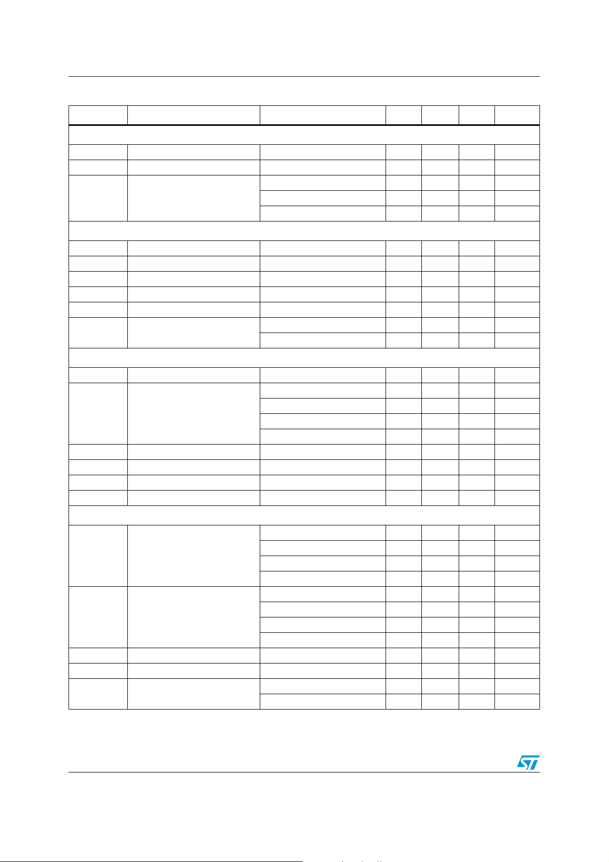
3 Electrical specifications
3.1 Thermal data
Table 3. Thermal data
Symbol Description Value Unit
R
th-j amb
Thermal resistance junction to ambient 114 °C/W
3.2 Absolute maximum ratings
Table 4. Absolute maximum ratings
Symbol Parameter Value Unit
V
V
in_max
T
T
S
amb
stg
Operating supply voltage 10.5 V
Maximum voltage for signal input pins 7 V
Operating ambient temperature -40 to 85 °C
Storage temperature range -55 to 150 °C
3.3 Electrical characteristics
VS = 8.5 V; T
specified
Table 5. Electrical characteristics
Symbol Parameter Test condition Min. Typ. Max. Unit
Supply
= -40 to 85 °C; RL= 10 kΩ; all gains = 0 dB; f = 1 kHz; unless otherwise
amb
V
s
I
s
Input selector
R
in
V
CL
S
IN
Differential stereo inputs
R
in
CMRR1
CMRR2
e
No
Supply voltage 7.5 8.5 10 V
Supply current 35 mA
Input resistance All single ended inputs
Clipping level Input gain = 0 dB 2 V
(1)
70 100 130 kΩ
RMS
Input separation 100 dB
Input resistance Differential 70 100 130 kΩ
=1 VRMS@ 1 kHz 46 60 dB
Common mode rejection ratio
for main source
Common mode rejection ratio
nd
source
for 2
Output noise @ speaker
outputs
V
CM
1 VRMS@ 10 kHz 46 60 dB
V
CM=
V
=1 VRMS@ 1 kHz 46 60 dB
CM
20 Hz-20 kHz, A-weighted;
all stages 0dB
12 µV
Doc ID 13698 Rev 4 9/46
Page 10
Electrical specifications TDA7719
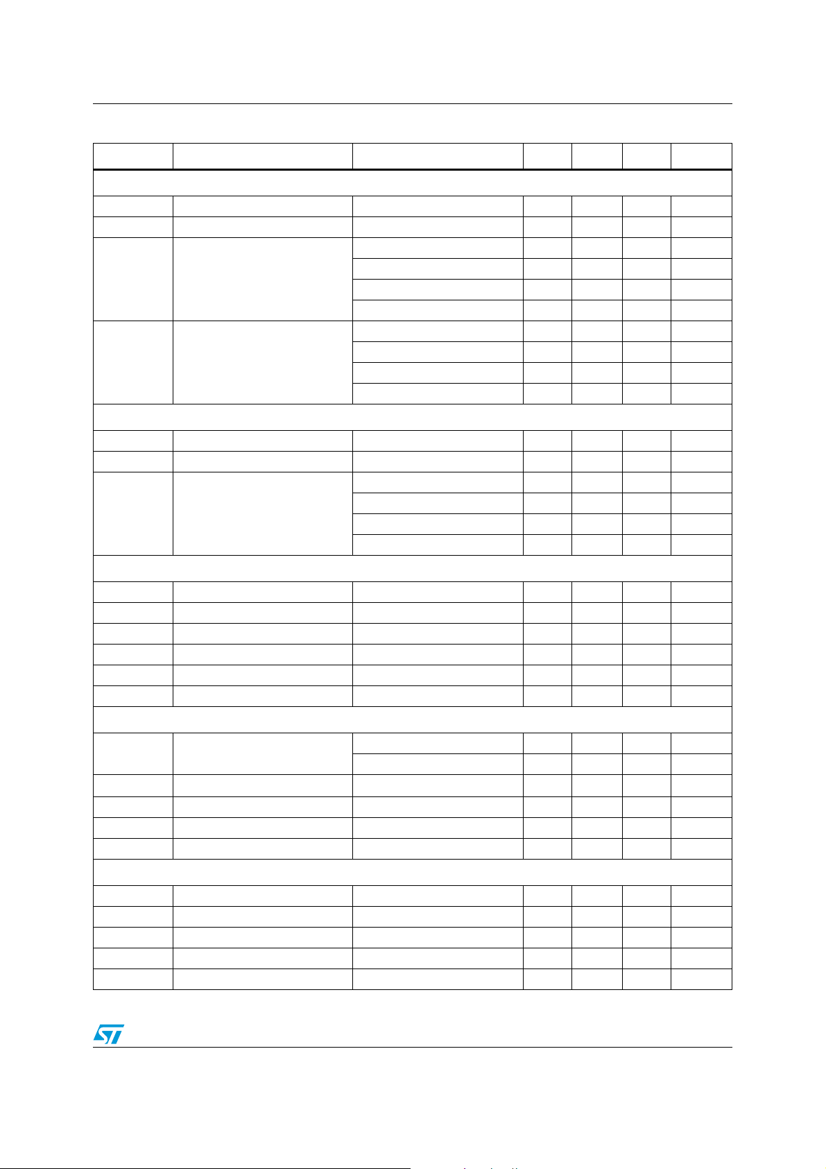
Table 5. Electrical characteristics (continued)
Symbol Parameter Test condition Min. Typ. Max. Unit
Loudness control
A
MAX
A
STEP
f
Peak
Volu m e con t ro l
Max attenuation 15 dB
Step resolution 1 dB
Peak frequency
f
P1
f
P2
f
P3
400 Hz
800 Hz
2400 Hz
G
A
A
V
MAX
MAX
STEP
E
A
E
T
DC
Max gain 15 dB
Max attenuation -15 dB
Step resolution 0.5 1 1.5 dB
Attenuation set error -0.75 0 +0.75 dB
Tracking error 2 dB
DC steps
Soft mute
A
MUTE
T
V
TH Low
V
TH High
R
V
D
PU
PU
Mute attenuation 80 100 dB
Delay time
Low threshold for SM pin 1 V
High threshold for SM pin 2.5 V
Internal pull-up resistor 32 45 58 kΩ
Internal pull-up Voltage 3.3 V
Bass control
Fc Center frequency
Q
BASS
C
RANGE
A
STEP
DC
GAIN
Quality factor
Control range ±14 ±15 ±16 dB
Step resolution 0.5 1 1.5 dB
Bass-DC-gain
Adjacent attenuation steps 0.1 3 mV
From 0 dB to G
MIN
0.5 5 mV
T1 0.48 ms
T2 0.96 ms
T3 8 ms
T4 16 ms
f
C1
f
C2
f
C3
f
C4
Q
1
Q
2
Q
3
Q
4
54 60 66 Hz
72 80 88 Hz
90 100 110 Hz
180 200 220 Hz
0.9 1 1.1
1.1 1.25 1.4
1.3 1.5 1.7
1.8 2 2.2
DC = off -1 0 +1 dB
DC = on, Gain =
±15 dB ±4.4 dB
10/46 Doc ID 13698 Rev 4
Page 11
TDA7719 Electrical specifications
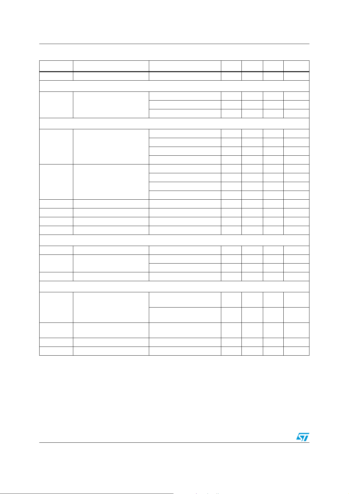
Table 5. Electrical characteristics (continued)
Symbol Parameter Test condition Min. Typ. Max. Unit
Middle control
C
RANGE
A
STEP
f
c
Q
BASS
Treble control
Control range ±14 ±15 ±16 dB
Step resolution 0.5 1 1.5 dB
Center frequency
Quality factor
f
C1
f
C2
f
C3
f
C4
Q
1
Q
2
Q
3
Q
4
400 500 600 Hz
0.8 1 1.2 kHz
1.2 1.5 1.8 kHz
22.53 kHz
0.45 0.5 0.55
0.65 0.75 0.85
0.9 1 1.1
1.1 1.25 1.4
C
RANGE
A
STEP
f
c
Clipping level ±14 ±15 ±16 dB
Step resolution 0.5 1 1.5 dB
Center frequency
Speaker attenuators
A
A
A
STEP
A
MUTE
V
MIN
MAX
E
DC
E
Min attenuation -1 0 1 dB
Max attenuation -89 -79 -69 dB
Step resolution 0.5 1 1.5 dB
Mute attenuation 80 90 dB
Attenuation set error 2 dB
DC steps Adjacent attenuation steps 0.1 5 mV
Audio outputs
Clipping level
Output impedance 30 100
Output load resistance 2 kΩ
Output load capacitor 10 nF
DC voltage level 3.8 4.0 4.2 V
R
V
V
CL
OUT
R
L
C
L
DC
Subwoofer attenuator
f
C1
f
C2
f
C3
f
C4
81012kHz
10 12.5 15 kHz
12 15 18 kHz
14 17.5 21 kHz
d = 0.3%; Byte8_D6=1 2 V
d = 1%; Byte8_D6=0 2.2 V
RMS
RMS
Ω
G
MAX
A
A
STEP
A
MUTE
MAX
E
E
Max gain 141516 dB
Max attenuation -83 -79 -75 dB
Step resolution 0.5 1 1.5 dB
Mute attenuation 80 90 dB
Attenuation set error 2 dB
Doc ID 13698 Rev 4 11/46
Page 12
Electrical specifications TDA7719
Table 5. Electrical characteristics (continued)
Symbol Parameter Test condition Min. Typ. Max. Unit
V
DC
Subwoofer lowpass
f
LP
DC offset detection circuit
V
th
t
sp
I
CHDCErr
I
DISDCErr
V
OutH
V
OutH
Level meter
DC steps Adjacent attenuation steps 0.1 5 mV
Lowpass corner frequency
f
f
f
LP1
LP2
LP3
72 80 88 Hz
108 120 132 Hz
144 160 176 Hz
V1 ±25 mV
Zero comp window size
V2 ±50 mV
V3 ±75 mV
V4 ±100 mV
11 µs
Max rejected spike length
22 µs
33 µs
44 µs
DCErr charge current 5 µA
DCErr discharge current 5 mA
DCErr high volotage 3.3 V
DCErr low voltage 100 mV
Vout Output voltage range 0 3.3 V
= 1 Vrms 1.6 V
V
V
LEVEL
T
DEL
Output level
Analog output delay time 2 µs
in
= AC grounded 0 V
V
in
General
BW = 20 Hz to 20 kHz
e
NO
Output noise
A-Weighted, all gain = 0 dB
BW = 20 Hz - 20 kHz
A-Weighted, output muted
S/N Signal to noise ratio
D Distortion V
S
C
1. When DC offset detector is not used, the impedance of mono single-ended input is 50 kΩ instead of 100 kΩ.
Channel separation left/right 90 dB
all gain = 0 dB, A-weighted;
= 2 V
V
o
RMS
IN
=1 V
all stages 0dB 0.01 %
RMS;
12 µV
6µV
104 dB
12/46 Doc ID 13698 Rev 4
Page 13
TDA7719 Description
4 Description
4.1 Input configuration
4.1.1 Front and rear selector
The input stage (Main source and 2nd source) is configurable to adapt to different
application. There are 7 different configurations which provide different input structure and
different number of input sources as shown below.
● 4 x QD,
● 2 x QD + 3 x SE,
● 1 x QD + 5 x SE,
● 1 x QD + 3 x SE + 2 x MD,
● 3 x QD + 1 x FD,
● 3 x QD + 2 x SE,
● 1 x QD + 2 x SE + 1 x FD + 1 x MD,
● 1 x QD + 3 x SE + 1 x FD
Note: QD = Quasi-Differential, SE = Single-ended input, FD = Full Differential, MD = mono
Differential
The configuration of the input stage is controlled by ‘Input Configuration’ bits in I
table (Byte0 Bit5~Bit7). The table below shows the configuration of input pins in different
configurations.
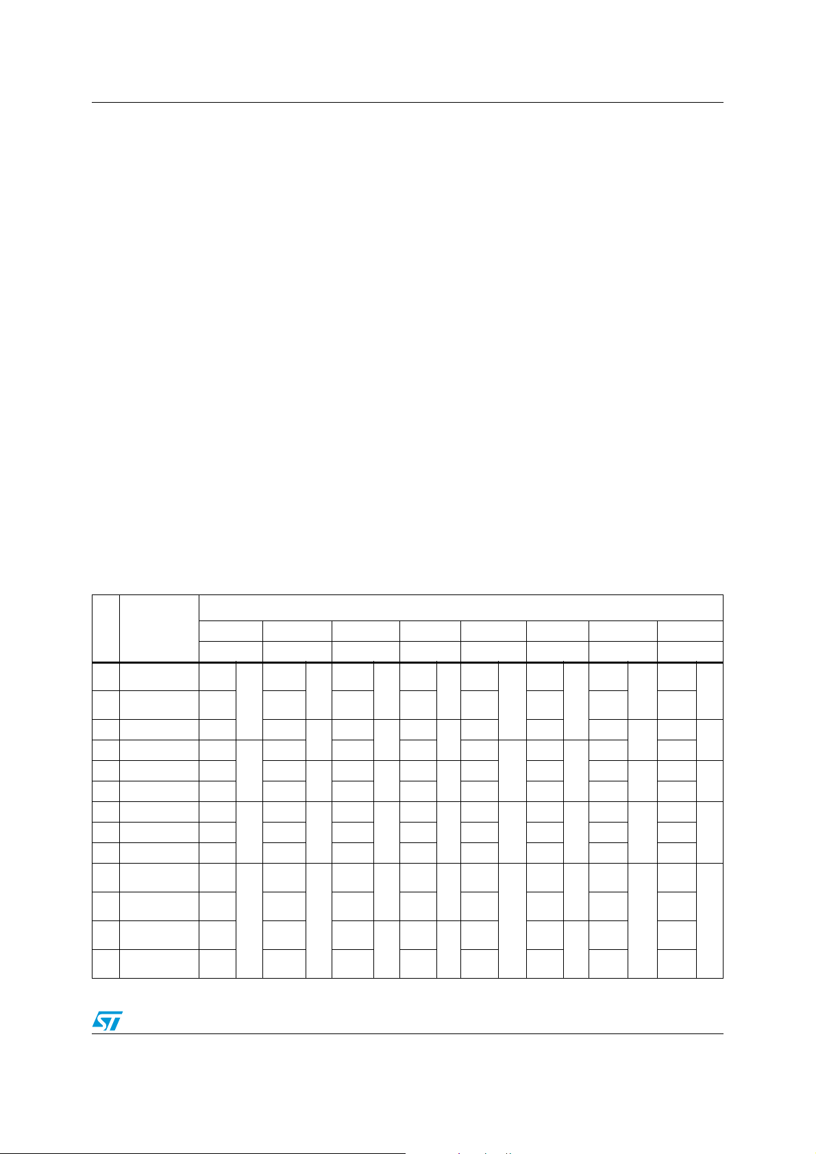
Table 6. Input pin configuration
Pin Pin name
QD1L_SE1L
1
_MD3+
QD1R_SE1R
2
_MD3-
QD1G_SE2L QD1G SE2L
3
QD2G_SE2R QD2G
4
QD2L_SE3L QD2L SE3L
5
QD2R_SE3R QD2R SE3R SE3R SE3R QD2R QD2R SE3R SE3R
6
QD3L QD3L
7
QD3G QD3G QD3G QD3G QD3G QD3G QD3G QD3G QD3G
8
QD3R QD3R QD3R QD3R QD3R QD3R QD3R QD3R QD3R
9
QD4L_FD4+
10
_SE4L_MD1+
QD4G_FD4L
11
_SE4R_MD1-
QD4G_FD4R_S
12
E5L_MD2-
QD4R_FD4R+_
13
SE5R_MD2+
Configuration bits (Byte0 Bit7~Bit5)
"000" "001" "010" "011" "100" "101" "110" "111"
CFG0 CFG1 CFG2 CFG3 CFG4 CFG5 CFG6 CFG7
QD1L
QD1R SE1R SE1R SE1R QD1R QD1R MD3- SE1R
QD4L
QD4G QD4G SE4R MD1- FD4L- SE4R FD4L- FD4L-
QD4G QD4G SE5L
QD4R QD4R SE5R MD2+
SE1L
IN0
SE2R SE2R SE2R QD2G
IN1
QD3L
IN2
QD4L
IN3
IN0
IN4
IN1
IN2
IN3
SE1L
SE2L
SE3L
QD3L
SE4L
IN0
IN4
IN1
IN2
IN5
IN6
SE1L
SE2L
SE3L
QD3L
MD1+
MD2-
QD1L
IN0
QD1G QD1G SE2L
IN4
QD2L QD2L SE3L
IN1
QD3L
IN2
FD4L+
IN3
FD4R- SE5L
IN3
FD4R
+
QD1L
IN0
QD2G
IN1
QD3L
IN2
SE4L
IN3
SE5R FD4R+ FD4R+
MD3+
IN0
SE2R SE2R
IN1
QD3L
IN2
FD4L+
IN5
FD4R- FD4R-
IN6
IN7
IN4
IN1
IN2
IN3
2
C control
SE1L
SE2L
SE3L
QD3L
FD4L+
IN0
IN4
IN1
IN2
IN3
Doc ID 13698 Rev 4 13/46
Page 14
Description TDA7719
With different input configuration, the input source can be selected with input selector
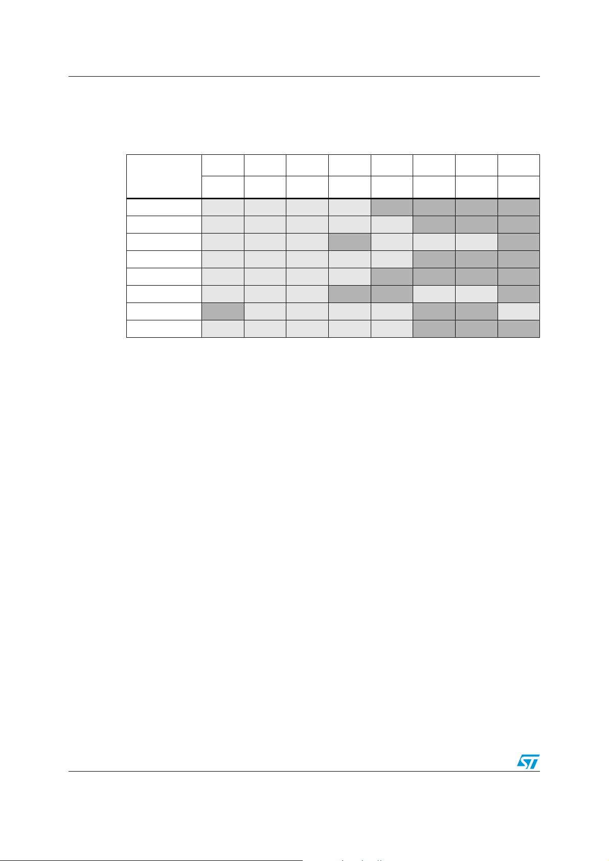
(Byte0/1 Bit0~Bit2). The following matrix defines the selector configuration of different input
sources dependant on the configuration bits.
Table 7. Selector configuration matrix
Selector Bits
000 001 010 011 100 101 110 111
(Byte0/1
Bit2~Bit0)
CFG0
CFG1
CFG2
CFG3
CFG4
CFG5
CFG6
CFG7
IN0IN1IN2IN3IN4IN5IN6IN7
QD1 QD2 QD3 QD4 NA NA NA NA
SE1 SE3 QD3 QD4 SE2 NA NA NA
SE1 SE3 QD3 NA SE2 SE4 SE5 NA
SE1 SE3 QD3 MD1/2 SE2 NA NA NA
QD1 QD2 QD3 FD NA NA NA NA
QD1 QD2 QD3 NA NA SE4 SE5 NA
NA SE3 QD3 FD SE2 NA NA MD3
SE1 SE3 QD3 FD SE2 NA NA NA
Note: In each configuration, only the light grey cells are allowed. The dark grey cells are not
allowed.
MD1/MD2 selection is defined by extra bit – ‘MD1/2 selection’ in I
2
C control table (Bit3 of
Byte0/1).
The input stage can be configured to 0dB or 3dB gain with I
2
C bus. The 0dB configuration
allows up to 2Vrms input signal level, while with 3dB gain, the internal signal will start to clip
when input signal level is higher than 1.414Vrms.
The Pin10~Pin13 can be configured as full differential input stage or quasi-differential input.
When it is configured as quasi-differential input, both Pin11 and Pin12 are used as the QD
common input pins. These two pins must be connected together externally in application. In
this case the input impedance of QD4 common is reduced to 50k
Ω (half of QD4 left and
right input). The diagram below shows both QD and FD configuration of QD4/FD4.
14/46 Doc ID 13698 Rev 4
Page 15

TDA7719 Description
Figure 3. QD and FD configuration of QD4/FD4
FD4L+
100k
FD4L-
100k
FD4R+
100k
FD4R-
100k
4.1.2 Direct path
The input pins can be configured as direct path mode by setting Byte1 Bit5~Bit7. In direct
path mode the input pins are connected to dedicated mono fader directly, all the filters and
volume are bypassed. Below is described the assignment of the input pins and output fader
in direct path mode:
FULL DIFFERENTIAL
1
2
1
2
QUASI DIFFERENTIAL
QD4L
100k
+
-
+
-
OUTL
OUTR
QD4G
QD4G
QD4R
100k
100k
100k
1
+
-
2
1
+
-
2
OUTL
OUTR
Pin5/QD2L --> OUTLF
Pin6/QD2R --> OUTRF
Pin7/QD3L --> OUTLR
Pin9/QD3R --> OUTRR
Pin10/FDL+_QD4L --> OUTL2
Pin13/FDR+_QD4R--> OUTR2
Note: 1 The configurations CFG2, CFG3 and CFG5 are not recommended in direct path mode.
Because in these 3 configurations SE4L/MD1+ and SE5R/MD2+ are connected to OUT2_L
and OUT2_R fader separately. In this case left and right channel of OUT2 belongs to
different input sources.
2 If the direct path is chosen, the input pins have to be used as single ended pins. In case of
differential inputs the ground or minus pins must be connect to GND by AC short.
3 Inputs in direct path mode are also selectable with front and rear selector.
Doc ID 13698 Rev 4 15/46
Page 16

Description TDA7719
4.2 Mixing
The device provides mixing function which allows the mixing source mixed into front and
rear speaker output independently. The mixing source can be any single-ended input,
mono-differential input or beep input (Mono single-ended input when DC offset detector is
not used). In order to adjust the level of mixing signal, the mixing selector is followed with a
0 dB~-31 dB attenuator. The maximum mixing input signal level is 1.6 Vrms for single-ended
input and mono-differential input. For beep input, the maximum input signal level is about
1.4 Vrms. The block diagram of the mixing function is shown below.
Figure 4. Block diagram of mixing stage
SE Inputs
MD Inputs
Beep
Mixing
Selector
0~-31dB
Speaker
Attenuator
Since the input stage of this device has different configurations, the corresponding sources
for mixing selector are also different according to the configurations. The following table
defines the available sources for mixing under different configurations.
Table 8. Available sources for mixing
Mix selector bits
(Byte2 Bit2~Bit0)
CFG0
CFG1
CFG2
000 001 010 011 100 101 110 111
MixIN0 MixIN1 MixIN2 MixIN3 MixIN4 MixIN5 MixIN6 MixIN7
NA NA NA NA NA NA Beep Mute
SE1 SE2 SE3 NA NA NA Beep Mute
SE1 SE2 SE3 SE4 SE5 NA Beep Mute
CFG3
CFG4
CFG5
CFG6
CFG7
SE1 SE2 SE3 MD1 NA MD2 Beep Mute
NA NA NA NA NA NA Beep Mute
NA NA NA SE4 SE5 NA Beep Mute
MD3 SE2 SE3 NA NA NA Beep Mute
SE1 SE2 SE3 NA NA NA Beep Mute
Note: Only light grey cells are allowed mixing input. The dark grey cells are not allowed.
The beep input is available only when DC offset detector function is not used.
16/46 Doc ID 13698 Rev 4
Page 17

TDA7719 Description
4.3 Loudness
There are four parameters programmable in the loudness stage:
4.3.1 Loudness attenuation
Figure 5 shows the attenuation as a function of frequency at fP = 400 Hz
Figure 5. Loudness attenuation @ f
4.3.2 Peak frequency
Figure 6 shows the four possible peak-frequencies at 400, 800 and 2400 Hz
Figure 6. Loudness center frequencies @ Attn. = 15 dB.
= 400 Hz.
P
Doc ID 13698 Rev 4 17/46
Page 18

Description TDA7719
4.3.3 High frequency boost
Figure 7 shows the different Loudness shapes in low and high frequency boost.
Figure 7. Loudness attenuation, f
4.3.4 Flat mode
In flat mode the loudness stage works as a 0dB to -15dB attenuator.
=2.4 kHz
c
4.4 SoftMute
The digitally controlled SoftMute stage allows muting/demuting the signal with a I2C-bus
programmable slope. The mute process can either be activated by the SoftMute pin or by
the I
regions (see Figure 8).
For timing purposes the Bit0 of the I
until the end of demuting.
Figure 8. SoftMute timing
1. A started Mute action is always terminated and could not be interrupted by a change of the mute signal.
2
C-bus. This slope is realized in a special S-shaped curve to mute slow in the critical
2
C-bus output register is set to 1 from the start of muting
1
EXT.
MUTE
+SIGNAL
REF
-SIGNAL
1
2
I
C BUS
OUT
TimeD97AU634
18/46 Doc ID 13698 Rev 4
Page 19

TDA7719 Description
4.5 Softstep volume
When the volume-level is changed audible clicks could appear at the output. The root cause
of those clicks could either be a DC Offset before the volume-stage or the sudden change of
the envelope of the audio signal. With the Softstep feature both kinds of clicks could be
reduced to a minimum and are no more audible. The blend-time from one step to the next is
programmable as 5 ms or 10 ms. The softstep control is described in detail in Chapter 4.10.
4.6 Bass
There are four parameters programmable in the bass stage:
4.6.1 Bass attenuation
Figure 9 shows the attenuation as a function of frequency at a center frequency of 80 Hz.
Figure 9. Bass Control @ f
4.6.2 Bass center frequency
Figure 10 shows the four possible center frequencies 60, 80, 100 and 200 Hz.
Figure 10. Bass center frequencies @ gain = 14 dB, Q = 1
= 80 Hz, Q = 1
c
Doc ID 13698 Rev 4 19/46
Page 20

Description TDA7719
4.6.3 Bass quality factors
Figure 11 shows the four possible quality factors 1, 1.25, 1.5 and 2.
Figure 11. Bass quality factors @ gain = 14 dB, f
4.6.4 DC mode
In this mode the DC gain is increased by 4.4 dB. In addition the programmed center
frequency and quality factor is decreased by 25 % which can be used to reach alternative
center frequencies or quality factors.
Figure 12. Bass normal and DC mode @ Gain = 14 dB, f
= 80 Hz
c
= 80 Hz
c
1. The center frequency, Q and DC-mode can be set fully independently.
20/46 Doc ID 13698 Rev 4
Page 21

TDA7719 Description
4.7 Middle
There are three parameters programmable in the middle stage:
4.7.1 Middle attenuation
Figure 13 shows the attenuation as a function of frequency at a center frequency of 1 kHz.
Figure 13. Middle control @ f
4.7.2 Middle center frequency
Figure 14 shows the four possible center frequencies 500 Hz, 1 kHz, 1.5 kHz and 2.5 kHz.
Figure 14. Middle center frequencies @ gain = 14d B, Q = 1
= 1 kHz, Q = 1
c
Doc ID 13698 Rev 4 21/46
Page 22

Description TDA7719
4.7.3 Middle quality factors
Figure 15 shows the four possible quality factors 0.5, 0.75, 1 and 1.25.
Figure 15. Middle quality factors @ gain = 14 dB, f
4.8 Treble
There are two parameters programmable in the treble stage:
4.8.1 Treble attenuation
= 1 kHz
c
Figure 16 shows the attenuation as a function of frequency at a center frequency of 17.5 kHz.
Figure 16. Treble Control @ fc = 17.5 kHz.
22/46 Doc ID 13698 Rev 4
Page 23

TDA7719 Description
4.8.2 Treble center frequency
Figure 17 shows the four possible center frequencies 10 k, 12.5 k, 15 k and 17.5 kHz.
Figure 17. Treble center frequencies @ gain = 14 dB
4.9 Subwoofer Filter
The subwoofer lowpass filter has Butterworth characteristics with programmable cut-off
frequency (80 / 120 / 160 Hz). The output phase can be selected between 0 deg and
180 deg. The input of subwoofer takes signal from bass filter output or output of input mux.
Figure 18. Subwoofer control
Doc ID 13698 Rev 4 23/46
Page 24

Description TDA7719
4.10 Softstep control
In this device, the softstep function is available for volume, speaker, loudness, treble, middle
and bass block. With softstep function, the audible noise of DC offset or the sudden change
of signal can be avoided when adjusting gain setting of the block.
For each block, the softstep function is controlled by softstep on/off control bit in the control
table. The softstep transient time selection (5 ms or 10 ms) is common for all blocks and it is
controlled by softstep time control bit. The softstep operation of all blocks has a common
centralized control. In this case, a new softstep operation can not be started before the
completion previous softstep.
There are two different modes to activate the softstep operation. The softstep operation can
be started right after I
2
C data sending, or the softstep can be activated in parallel after data
sending of several different blocks. The two modes are controlled by the ‘act bit’ (it is
normally bit7 of the byte.) of each byte. When act bit is ‘0’, which means action, the softstep
is activated right after the date byte is sent. When the act bit is ‘1’, which means wait, the
block goes to wait for softstep status. In this case, the block will wait for some other block to
activate the operation. The softstep operation of all blocks in wait status will be done
together with the block which activate the softstep. With this mode, all specific blocks can do
the softstep in parallel. This avoids waiting when the softstep is operated one by one.
Chip Addr Sub Addr 0xxxxxxx
|
↑ Softstep start here
Chip Addr Sub Addr 1xxxxxxx 1xxxxxxx ...... 0xxxxxxx
|
↑ Softstep start
here for all
1. It is not allowed to cross 0 dB with softstep directly. From plus gain to minus gain, it
must go to +0 dB first, then destination. From minus gain to plus gain, it must go to 0 dB first, and then destination.
2. When one block is in ‘wait for softstep’ status, it is not allowed to send data to this block
again before its softstep is completed.
3. To know if there is a softstep in operation, it is possible to monitor the ‘busy’ signal by
2
I
C transmission mode (Section 5.1.2). When softstep is busy (busy=0), it is better to
wait before sending new data until it is free (busy=1).
24/46 Doc ID 13698 Rev 4
Page 25

TDA7719 Description
4.11 DC offset detector and level meter option
This device provide DC offset detector function and level meter function option. In one
specific application, only one of the function can be used. The configuration of the function
is controlled by I
2
C bus (Byte3 Bit7).
When the device uses DC offset detector function, Pin22, Pin27 and Pin28 are used as
WinTC, DCErr and WinIN for DC offset detector. When it is configured as level meter, DCErr
becomes level meter output. In the mean time, WinIN is used as beep input (Mono singleended input for mixing), and WinTC becomes a reference voltage output (4 V external DC
voltage or 3.3 V internal reference voltage).
4.12 DC offset detector
Using the DC offset detection circuit (Figure 19) an offset voltage difference between the
audio power amplifier and the TDA7719's Front and Rear outputs can be detected,
preventing serious damage to the loudspeakers. The circuit compares whether the signal
crosses the zero level inside the audio power at the same time as in the speaker cell. The
output of the zero-window-comparator of the power amplifier must be connected with the
WinIn-input of the TDA7719. The WinIn-input has an internal pull-up resistor connected to
5.5Volts. It is recommended to drive this pin with open-collector outputs only.
To compensate for errors at low frequencies the WinTC-pin are implemented, with external
capacitors introducing the same delay τ = 7.5kΩ * C
as the AC-coupling between the
ext
TDA7719 and the power amplifier introduces. For the zero window comparators, the time
constant for spike rejection as well as the threshold are programmable.
For electrical characteristics see Chapter 3 on page 9.
A low-active DC-offset error signal appears at the DCErr output if the next conditions are
both true:
a) Front and rear outputs are inside zero crossing windows.
b) The Input voltage VWinIn is logic low whenever at least one output of the power
amplifier is outside the zero crossing windows.
After power-on, the external attached capacitor is rapidly charged (fast-charge) to overcome
a false indication.
Doc ID 13698 Rev 4 25/46
Page 26

Description TDA7719
Figure 19. DC offset detection circuit (simplified)
4.13 Level meter
In case of not using DC offset detector, the three pins used for DCO can be configured as
other function. Pin27 (DC_Err / LMOUT) becomes the level meter output. The level meter
block takes signal after main input selector and mix signal into mono, then rectify the signal
and detect the peak of the signal. The output stage of level meter removes the DC voltage of
the signal and the output voltage level shows exactly the Vpeak of signal. Since the
discharge time constant of the level meter is quite slow, it is necessary to reset level meter
regularly (with I
2
C bus control Byte3 Bit6) to get correct peak information of the signal.
4.14 Output gain control
The output stage of the device can provide a option to have additional 1 dB gain in order to
boost the maximum output level to 2.2 Vrms with maximum 1 % distortion.
4.15 Audioprocessor testing
In the test mode, which can be activated by setting bit D7 of the I2C subaddress byte and bit
D0 of the testing-audioprocessor byte, several internal signals are available at the QD1L pin.
In this mode, the input resistance of 100 kΩ is disconnected from the pin. Internal signals
available for testing are listed in the data-byte specification.
26/46 Doc ID 13698 Rev 4
Page 27

TDA7719 Description
4.16 Test circuit (3 x QD + 1 x FD + DC offset detector)
Figure 20. Test circuit
Doc ID 13698 Rev 4 27/46
Page 28

I2C bus specification TDA7719
5 I2C bus specification
5.1 Interface protocol
The interface protocol comprises:
● a start condition (S)
● a chip address byte (the LSB determines read/write transmission)
● a subaddress byte
● a sequence of data (N-bytes + acknowledge)
● a stop condition (P)
● the max. clock speed is 400 kbits/s
● 3.3 V logic compatible
Figure 21. Switching characteristics
S = Start
ACK = Acknowledge
Table 9. I2C bus electrical characterisitics
Symbol Parameter Min Max Unit
f
SCL
V
IH
V
IL
t
HD,STA
t
SU,STO
t
LOW
t
HIGH
t
F
t
R
t
HD,DAT
t
SU,DAT
SCL clock frequency 400 kHz
High level input voltage 2.4 V
Low level input voltage 0.8 V
Hold time for START 0.6 µs
Setup time for STOP 0.6 µs
Low period for SCL clock 1.3 µs
High period for SCL clock 0.6 µs
Fall time for SCL/SDA 300 ns
Rise time for SCL/SDA 300 ns
Data hold time 0 ns
Data setup time 100 ns
28/46 Doc ID 13698 Rev 4
Page 29

TDA7719 I2C bus specification
Figure 22. I2C timing diagram
5.1.1 Receive mode
S 10 0010 0 R/W ACK TS X AI A4 A3 A2 A1 A0 ACK DATA ACK P
S = Start
R/W = "0" -> Receive Mode (Chip can be programmed by µP)
"1" -> Transmission Mode (Data could be received by µP)
ACK = Acknowledge
P = Stop
TS = Testing mode
AI = Auto increment
5.1.2 Transmission mode
S 1 0 0 0 1 0 0 R/W ACK X X X X X X BZ SM ACK P
SM = Soft mute activated for main channel
BZ = Softstep Busy (‘0’ = Busy)
X = Not used
The transmitted data is automatic updated after each ACK. Transmission can be repeated
without new chip address.
5.1.3 Reset condition
A Power-On-Reset is invoked if the supply voltage is below than 3.5V. After that the registers
are initialized to the default data written in following tables.
Doc ID 13698 Rev 4 29/46
Page 30

I2C bus specification TDA7719
Table 10. Subaddress (receive mode)
MSB LSB
Function
I2 I1 I0 A4 A3 A2 A1 A0
Testing Mode
0
1
x Not used
0
1
0 0 0 0 0 Input Configuration / Main Source Selector
000 0 12
0 0 0 1 0 Mixing Source / Mixing Gain
0 0 0 1 1 Mix Control / Level Meter / DC Offset Detector Config
0 0 1 0 0 Soft Mute / Others
001 01Soft Step I
0 0 1 1 0 Soft Step II / DC-detector
Off
On
Auto Increment Mode
Off
On
nd
Source Selector / Direct Path
0 0 1 1 1 Loudness
0 1 0 0 0 Volume / Output Gain
010 0 1Treble
010 1 0Middle
010 1 1Bass
0 1 1 0 0 Subwoofer / Middle / Bass
0 1 1 0 1 Speaker Attenuator Left Front
0 1 1 1 0 Speaker Attenuator Right Front
0 1 1 1 1 Speaker Attenuator Left Rear
1 0 0 0 0 Speaker Attenuator Right Rear
1 0 0 0 1 Subwoofer Attenuator Left
1 0 0 1 0 Subwoofer Attenuator Right
1 0 0 1 1 Testing Audio Processor 1
1 0 1 0 0 Testing Audio Processor 2
30/46 Doc ID 13698 Rev 4
Page 31

TDA7719 I2C bus specification
5.2 Data byte specification
The default power on status of the registers is written with underline.
Table 11. Input configuration / main selector (0)
MSB LSB
D7 D6 D5 D4 D3 D2 D1 D0
0
0
0
0
1
1
1
1
Function
Main source selector
0
0
0
0
1
1
1
1
0
1
0
0
1
1
0
0
1
1
0
IN0
1
IN1
0
IN2
IN3
1
IN4
0
IN5
1
IN6
0
IN7
1
configuration for main selector
MD1/2
MD1
MD2
Main source input gain select
0
1
0dB
3dB
Input configuration
0
0
1
1
0
0
1
1
0
1
0
1
0
1
0
1
CFG0
CFG1
CFG2
CFG3
CFG4
CFG5
CFG6
CFG7
Note: For detailed input source and input stage configuration, please refer to Section 4.1.
Doc ID 13698 Rev 4 31/46
Page 32

I2C bus specification TDA7719
Table 12. 2
MSB LSB
D7 D6 D5 D4 D3 D2 D1 D0
nd
Source selector / direct path (1)
0
0
0
0
1
1
1
1
0
1
0
1
0
1
Function
nd
Source Selector
2
0
0
1
1
0
0
1
1
IN0
0
IN1
1
IN2
0
IN3
1
IN4
0
IN5
1
IN6
0
IN7
1
MD1/2 Configuration for 2
nd
Selector
MD1
MD2
nd
Source Input Gain Select
2
0dB
3dB
QD2 Bypass (Front)
on
Off
QD3 Bypass (Rear)
0
1
on
Off
QD4 Bypass (Subwoofer)
0
1
on
Off
Note: For detailed input source and input stage configuration, please refer to Section 4.1.
To active QD3 Bypass (Rear) function, it needs to set Byte3_D4 to “Direct Path / 2
also.
nd
Source”
32/46 Doc ID 13698 Rev 4
Page 33

TDA7719 I2C bus specification
Table 13. Mixing source / mixing gain (2)
MSB LSB
D7 D6 D5 D4 D3 D2 D1 D0
0
0
0
0
0
0
0
0
0
0
0
0
0
0
0
0
1
1
1
1
1
1
1
1
1
1
1
1
1
1
1
1
0
0
0
0
0
0
0
0
1
1
1
1
1
1
1
1
0
0
0
0
0
0
0
0
1
1
1
1
1
1
1
1
0
0
0
0
1
1
1
1
0
0
0
0
1
1
1
1
0
0
0
0
1
1
1
1
0
0
0
0
1
1
1
1
0
0
1
1
0
0
1
1
0
0
1
1
0
0
1
1
0
0
1
1
0
0
1
1
0
0
1
1
0
0
1
1
Function
Mixing Source Selector
0
0
0
0
1
1
1
1
0
0
1
1
0
0
1
1
0
IN0
1
IN1
0
IN2
1
IN3
0
IN4
1
IN5
0
IN6
1
IN7
Mixing Attenuator
0
1
0
1
0
1
0
1
0
1
0
1
0
1
0
1
0
1
0
1
0
1
0
1
0
1
0
1
0
1
0
1
0dB
-1dB
-2dB
-3dB
-4dB
-5dB
-6dB
-7dB
-8dB
-9dB
-10dB
-11dB
-12dB
-13dB
-14dB
-15dB
-16dB
-17dB
-18dB
-19dB
-20dB
-21dB
-22dB
-23dB
-24dB
-25dB
-26dB
-27dB
-28dB
-29dB
-30dB
-31dB
Doc ID 13698 Rev 4 33/46
Page 34

I2C bus specification TDA7719
Table 14. Mix control / level meter / dc offset detector configure (3)
MSB LSB
D7 D6 D5 D4 D3 D2 D1 D0
Mix to Front Left
0
On
1
Off
Mix to Front Right
0
1
On
Off
Mix to Rear Left
0
1
On
Off
Mix to Rear Right
0
1
On
Off
Rear Speaker Input Configuration
0
1
Direct Path / 2nd Source
Main Signal
Reference Output Select
0
1
Internal Vref (3.3V)
External Vref (4V
Level Meter Reset
0
1
Normal
Reset
Function
)
DC Offset Detector / Level Meter Config
0
1
Level Meter
DC Offset Detector
34/46 Doc ID 13698 Rev 4
Page 35

TDA7719 I2C bus specification
Table 15. Soft mute / others (4)
MSB LSB
D7 D6 D5 D4 D3 D2 D1 D0
0
1
0
0
1
1
0
1
0
1
0
1
0
1
Function
Soft Mute
0
On
1
Off
Pin Influence for Mute
Pin and IIC
IIC
Soft Mute Time
0.48ms
0.96ms
7.68ms
15.36ms
Subwoofer Input Configuration
Input Mux
Bass Output
Subwoofer Enable (OUTL3 & OUTR3)
On
Off
Fast Charge
0
1
On
Off
Anti-Alias Filter
0
1
On
Off (bypass)
Doc ID 13698 Rev 4 35/46
Page 36

I2C bus specification TDA7719
Table 16. SoftStep I (5)
MSB LSB
D7 D6 D5 D4 D3 D2 D1 D0
0
1
0
1
0
1
0
1
0
1
0
1
Loudness Soft Step
0
On
Off
1
Volume Soft Step
On
Off
Treble Soft Step
On
Off
Middle Soft Step
On
Off
Bass Soft Step
On
Off
Speaker LF Soft Step
On
Off
Speaker RF Soft Step
On
Off
Function
Speaker LR Soft Step
0
1
On
Off
36/46 Doc ID 13698 Rev 4
Page 37

TDA7719 I2C bus specification
Table 17. SoftStep II / DC detector (6)
MSB LSB
D7 D6 D5 D4 D3 D2 D1 D0
0
1
0
1
0
1
0
0
1
0
0
1
1
0
1
0
1
0
1
0
Function
Speaker RR Soft Step
0
on
1
off
Subwoofer Left Soft Step
on
off
Subwoofer Right Soft Step
on
off
Soft Step Time
5ms
10ms
Zero-comparator Window size
±100mV
±75mV
±50mV
Spike rejection time constant
11µs
22 µs
33 µs
44 µs
Doc ID 13698 Rev 4 37/46
Page 38

I2C bus specification TDA7719
Table 18. Loudness (7)
MSB LSB
D7 D6 D5 D4 D3 D2 D1 D0
0
0
:
1
1
0
0
1
1
0
1
0
1
0
0
:
1
1
0
0
:
1
1
0
1
0
1
Attenuation
0
0dB
1
-1dB
:
:
0
-14dB
-15dB
1
Center Frequency
Flat
400Hz
800Hz
2400Hz
High Boost
on
off
Soft Step Action
act
wait
Function
Table 19. Volume / output gain (8)
MSB LSB
D7 D6 D5 D4 D3 D2 D1 D0
x Not used
0
1
0
1
Function
Gain/Attenuation
0
0
:
0
0
1
1
:
1
1
0
0
:
1
1
1
1
:
0
0
0
0
:
1
1
1
1
:
0
0
0
0
:
1
1
1
1
:
0
0
0
-15dB
1
-14dB
:
:
0
-1dB
1
0dB
1
0dB
0
+1dB
:
:
+14dB
1
+15dB
0
Output Gain
1dB
0dB
Soft Step Action
act
wait
38/46 Doc ID 13698 Rev 4
Page 39

TDA7719 I2C bus specification
Table 20. Treble filter (9)
MSB LSB
D7 D6 D5 D4 D3 D2 D1 D0
0
0
:
0
0
1
1
:
1
1
0
0
1
1
0
1
0
1
0
0
:
1
1
1
1
:
0
0
0
0
:
1
1
1
1
:
0
0
0
0
:
1
1
1
1
:
0
0
0
1
Gain/Attenuation
0
-15dB
1
-14dB
:
:
0
-1dB
1
0dB
1
0dB
0
+1dB
:
:
+14dB
1
+15dB
0
Treble Center Frequency
10.0kHz
12.5kHz
15.0kHz
17.5kHz
Soft Step Action
act
wait
Function
Table 21. Middle filter (10)
MSB LSB
D7 D6 D5 D4 D3 D2 D1 D0
0
0
1
1
0
1
Function
Gain/Attenuation
0
0
:
0
0
1
1
:
1
1
0
0
:
1
1
1
1
:
0
0
0
0
:
1
1
1
1
:
0
0
0
0
:
1
1
1
1
:
0
0
0
-15dB
1
-14dB
:
:
0
-1dB
1
0dB
1
0dB
0
+1dB
:
:
+14dB
1
+15dB
0
Middle Q Factor
0
1
0
1
0.5
0.75
1
1.25
Soft Step Action
act
wait
Doc ID 13698 Rev 4 39/46
Page 40

I2C bus specification TDA7719
Table 22. Bass filter (11)
MSB LSB
D7 D6 D5 D4 D3 D2 D1 D0
0
0
:
0
0
1
1
:
1
1
0
0
1
1
0
1
0
1
0
0
:
1
1
1
1
:
0
0
0
0
:
1
1
1
1
:
0
0
0
0
:
1
1
1
1
:
0
0
0
1
Gain/Attenuation
0
-15dB
1
-14dB
:
:
0
-1dB
1
0dB
1
0dB
0
+1dB
:
:
+14dB
1
+15dB
0
Bass Q Factor
1.0
1.25
1.5
2.0
Soft Step Action
act
wait
Function
Table 23. Subwoofer / middle / bass (12)
MSB LSB
D7 D6 D5 D4 D3 D2 D1 D0
0
0
1
1
0
0
1
1
0
1
0
1
0
1
Function
Subwoofer Cut-off Frequency
0
0
1
1
0
flat
1
80Hz
0
120Hz
160Hz
1
Subwoofer Output Phase
0
1
180 deg
0 deg
Middle Center Frequency
0
1
0
1
500Hz
1000Hz
1500Hz
2500Hz
Bass Center Frequency
60Hz
80Hz
100Hz
200Hz
Bass DC Mode
on
off
40/46 Doc ID 13698 Rev 4
Page 41

TDA7719 I2C bus specification
Table 24. Speaker attenuation (LF/RF/LR/RR) (13-16)
MSB LSB
D7 D6 D5 D4 D3 D2 D1 D0
Gain/Attenuation
0
0
:
0
0
0
:
1
1
1
0
0
:
0
0
0
:
0
0
1
0
0
:
0
1
1
:
1
1
x
0
0
:
1
0
0
:
1
1
x
0
0
:
1
0
0
:
1
1
x
0
0
:
1
0
0
:
1
1
x
0
0dB
1
0dB
:
:
1
0dB
0
0dB
1
-1dB
:
:
0
-78dB
1
-79dB
x
mute
Soft Step Action
0
1
Table 25. Subwoofer attenuation (subwoofer L/subwoofer R) (17-18)
act
wait
MSB LSB
D7 D6 D5 D4 D3 D2 D1 D0
Function
Function
Gain/Attenuation
0
0
:
0
0
0
:
1
1
1
0
0
:
0
0
0
:
0
0
1
0
0
:
0
1
1
:
1
1
x
0
0
:
1
0
0
:
1
1
x
0
0
:
1
0
0
:
1
1
x
0
0
:
1
0
0
:
1
1
x
0
+0dB
1
+1dB
:
:
1
+15dB
0
-0dB
1
-1dB
:
:
0
-78dB
1
-79dB
x
mute
Soft Step Action
0
1
act
wait
Doc ID 13698 Rev 4 41/46
Page 42

I2C bus specification TDA7719
Table 26. Testing audio processor 1 (19)
MSB LSB
D7 D6 D5 D4 D3 D2 D1 D0
Audio Processor Testing Mode
0
off
on
1
Test Multiplexer at QD1L
0
0
0
0
0
0
0
0
1
1
1
1
1
1
1
1
0
0
0
0
1
1
1
1
0
0
0
0
1
1
1
1
0
0
1
1
0
0
1
1
0
0
1
1
0
0
1
1
0
1
0
1
0
1
0
1
0
1
0
1
0
1
0
1
DCDet Vth High
DCDet Vth Low
VolumeoutL
IntZeroErr
InGainL
LoudoutL
BassoutL
MidoutL
Ref5V5
VGB1.26
SMCLK
Tr e bl e o u tL
SSCLK
Clock200k
REQ
SDCLK
Clock Fast Mode
0
1
on
Off
Clock Source
0
1
external (at mute pin)
Internal (200kHz)
x Not Used
1. The control bit needs both I2C test mode on & sub-address test mode on.
2. The control bit does not depend on test mode.
Function
(1)
(2)
(2)
42/46 Doc ID 13698 Rev 4
Page 43

TDA7719 I2C bus specification
Table 27. Testing audio processor 2 (20)
MSB LSB
D7 D6 D5 D4 D3 D2 D1 D0
Test Architecture
normal
0
Split
1
Oscillator Clock
0
1
400kHz
800kHz
Softstep Curve
0
1
S-Curve
Linear Curve
Manual Set Busy Signal
0
0
1
1
0
1
0
1
Auto
Auto
0
1
Request for Clk Generator
0
0
1
1
0
1
0
1
Allow
Allow
Stopped
Stopped
xxx Not Used
1. The control bit needs sub-address test mode on
2. The control bit does not depend on test mode.
Function
(1)
(2)
(2)
(1)
(1)
Doc ID 13698 Rev 4 43/46
Page 44

Package information TDA7719
6 Package information
In order to meet environmental requirements, ST offers these devices in different grades of
ECOPACK
®
packages, depending on their level of environmental compliance. ECOPACK
®
specifications, grade definitions and product status are available at: www.st.com.
ECOPACK
®
is an ST trademark.
Figure 23. TSSOP28 mechanical data and package dimensions
DIM.
A 1.200 0.047
A1 0.050 0.150 0.002 0.006
A2 0.800 1.000 1.050 0.031 0.039 0.041
b 0.190 0.300 0.007 0.012
c 0.090 0.200 0.004 0.008
1
D
E 6.200 6.400 6.600 0.244 0.252 0.260
1
E1
e 0.650 0.026
L 0.450 0.600 0.750 0.018 0.024 0.030
L1 1.000 0.039
k 0˚ (min.), 8˚ (max.)
aaa 0.100 0.004
Note: 1. D and E1 does not include mold flash or protrusions.
mm inch
MIN. TYP. MAX. MIN. TYP. MAX.
9.600 9.700 9.800 0.378 0.382 0.386
4.300 4.400 4.500 0.170 0.173 0.177
Mold flash or potrusions shall not exceed 0.15mm
(.006inch) per side.
OUTLINE AND
MECHANICAL DATA
TSSOP28
Thin Shrink Small Outline Package
JEDEC MO-153-AC
44/46 Doc ID 13698 Rev 4
0128292 B
Page 45

TDA7719 Revision history
7 Revision history
Table 28. Document revision history
Date Revision Changes
16-Jul-2007 1 Initial release.
Added and updated the values on the Ta bl e 5: E l e c t r ic a l
07-Jan-2007 2
30-Jul-2008 3 Updated Table 5: Electrical characteristics.
23-Apr-2009 4
characteristics.
Document status promoted from preliminary data to datasheet.
Updated Figure 1: Block circuit diagram on page 6.
Updated Section 4.1: Input configuration on page 13.
Added Section 4.1.2: Direct path on page 15.
Added Figure 21: Switching characteristics on page 28,
Tab l e 9 : I
2
C bus electrical characterisitics on page 28 and Figure 22:
I2C timing diagram on page 29.
Doc ID 13698 Rev 4 45/46
Page 46

TDA7719
Please Read Carefully:
Information in this document is provided solely in connection with ST products. STMicroelectronics NV and its subsidiaries (“ST”) reserve the
right to make changes, corrections, modifications or improvements, to this document, and the products and services described herein at any
time, without notice.
All ST products are sold pursuant to ST’s terms and conditions of sale.
Purchasers are solely responsible for the choice, selection and use of the ST products and services described herein, and ST assumes no
liability whatsoever relating to the choice, selection or use of the ST products and services described herein.
No license, express or implied, by estoppel or otherwise, to any intellectual property rights is granted under this document. If any part of this
document refers to any third party products or services it shall not be deemed a license grant by ST for the use of such third party products
or services, or any intellectual property contained therein or considered as a warranty covering the use in any manner whatsoever of such
third party products or services or any intellectual property contained therein.
UNLESS OTHERWISE SET FORTH IN ST’S TERMS AND CONDITIONS OF SALE ST DISCLAIMS ANY EXPRESS OR IMPLIED
WARRANTY WITH RESPECT TO THE USE AND/OR SALE OF ST PRODUCTS INCLUDING WITHOUT LIMITATION IMPLIED
WARRANTIES OF MERCHANTABILITY, FITNESS FOR A PARTICULAR PURPOSE (AND THEIR EQUIVALENTS UNDER THE LAWS
OF ANY JURISDICTION), OR INFRINGEMENT OF ANY PATENT, COPYRIGHT OR OTHER INTELLECTUAL PROPERTY RIGHT.
UNLESS EXPRESSLY APPROVED IN WRITING BY AN AUTHORIZED ST REPRESENTATIVE, ST PRODUCTS ARE NOT
RECOMMENDED, AUTHORIZED OR WARRANTED FOR USE IN MILITARY, AIR CRAFT, SPACE, LIFE SAVING, OR LIFE SUSTAINING
APPLICATIONS, NOR IN PRODUCTS OR SYSTEMS WHERE FAILURE OR MALFUNCTION MAY RESULT IN PERSONAL INJURY,
DEATH, OR SEVERE PROPERTY OR ENVIRONMENTAL DAMAGE. ST PRODUCTS WHICH ARE NOT SPECIFIED AS "AUTOMOTIVE
GRADE" MAY ONLY BE USED IN AUTOMOTIVE APPLICATIONS AT USER’S OWN RISK.
Resale of ST products with provisions different from the statements and/or technical features set forth in this document shall immediately void
any warranty granted by ST for the ST product or service described herein and shall not create or extend in any manner whatsoever, any
liability of ST.
ST and the ST logo are trademarks or registered trademarks of ST in various countries.
Information in this document supersedes and replaces all information previously supplied.
The ST logo is a registered trademark of STMicroelectronics. All other names are the property of their respective owners.
© 2009 STMicroelectronics - All rights reserved
STMicroelectronics group of companies
Australia - Belgium - Brazil - Canada - China - Czech Republic - Finland - France - Germany - Hong Kong - India - Israel - Italy - Japan -
Malaysia - Malta - Morocco - Philippines - Singapore - Spain - Sweden - Switzerland - United Kingdom - United States of America
www.st.com
46/46 Doc ID 13698 Rev 4
 Loading...