

Page 1
5W+5W AMPLIFIER WITH DC VOLUME CONTROL
■ 5+5W OUTPUT POWER
R
= 8Ω @THD = 10% VCC = 22V
L
■ ST-BY AND MUTE FUNCTIONS
■ LOW TURN-ON TURN-OFF POP NOISE
■ LINEAR VOLUME CONTROL DC COUPLED
WITH POWER OP. AMP.
■ NO BOUCHEROT CELL
■ NO ST_BY RC INPUT NETWORK
■ SINGLE SUPPLY RANGING UP TO 35V
■ SHORT CIRCUIT PROTECTION
■ THERMAL OVERLOAD PROTECTION
■ INTERNALLY FIXED GAIN
■ SOFT CLIPPING
■ VARIABLE OUTPUT AFTER VOLUME
CONTROL CIRCUIT
■ CLIPWA TT 1 5 P A C KA GE
DESCRIPTION
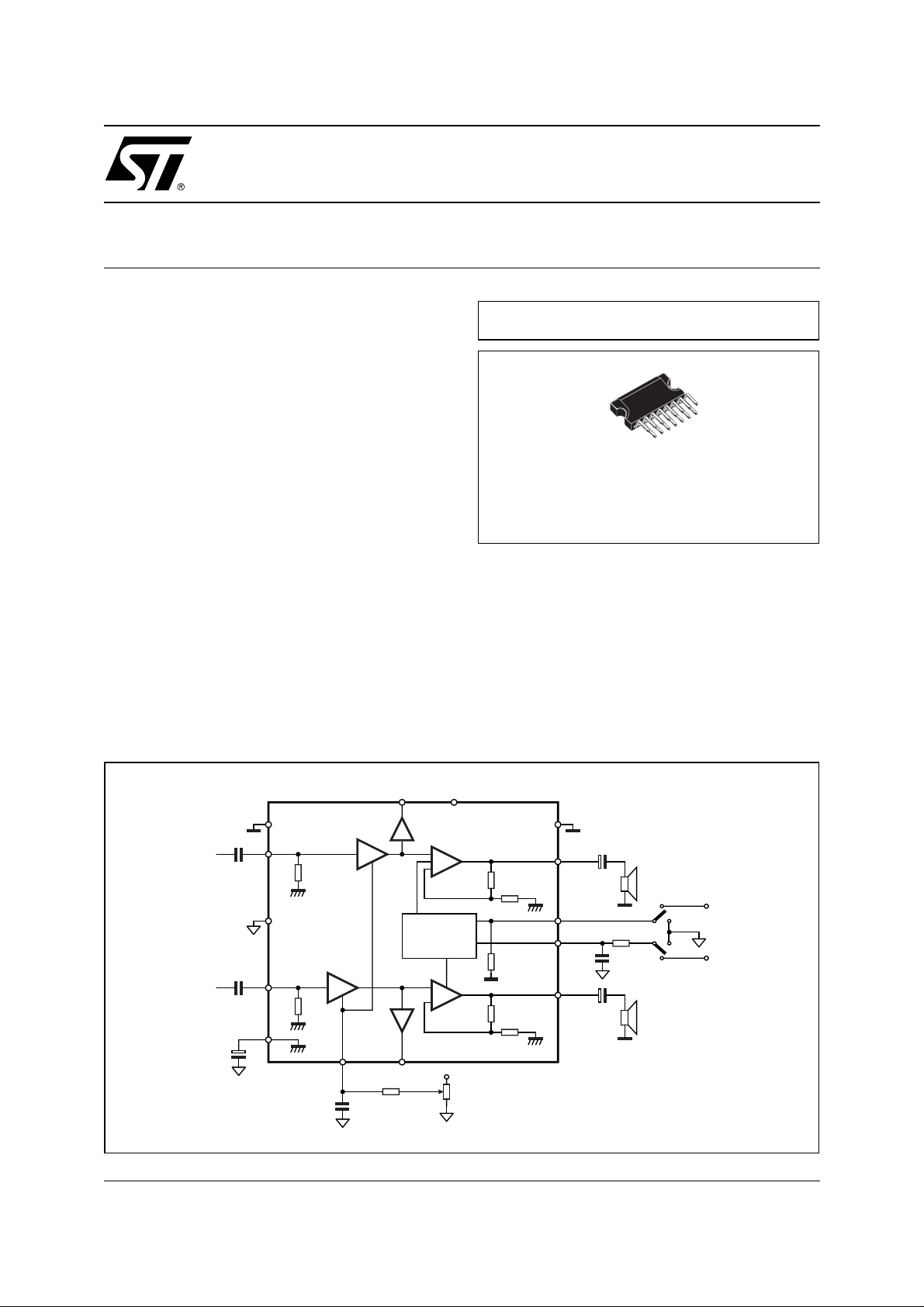
The TDA7496SA is a stereo 5+5W class AB power
TDA7496SA
PRODUCT PREVIEW
MULTIPOWER BI50II TECHNOLOGY
Clipwatt 15
ORDERING NUMBER: TDA7496SA
amplifier assembled i the @Clipwatt 15 package,
specially designed for high quality sound TV applications.
Features of the TDA7496SA include linear volume
control Stand-by and Mute functions.
The TDA7496SA is pin to pin compatible with
TDA7496, TDA7496S, TDA7496SA, TDA7495,
TDA7495SA, TDA7494S, TDA7494SA.
BLOCK DIAGRAM
VAROUT_R
PW_GND
INR
470nF
INL
470nF
470µF
S_GND
SVR 7
11
1
8
5
VOLUME
VOLUME
30K
VOLUME
34
100nF
VAROUT_L
300K
September 2003
This is preliminary information on a new product now in development. Details are subject to change without notice.
V
S
2
13
+
OP AMP
MUTE/STBY
PROTECTIONS
+
-30K
OP AMP
+5V
60K
D96AU440D
15
14
10
12
9
PW_GND
1000µF
OUTR
STBY
MUTE
OUTL
1000µF
10K
1µF
S1 ST-BY
S2 MUTE
+5V
S_GND
+5V
1/13
Page 2
TDA7496SA
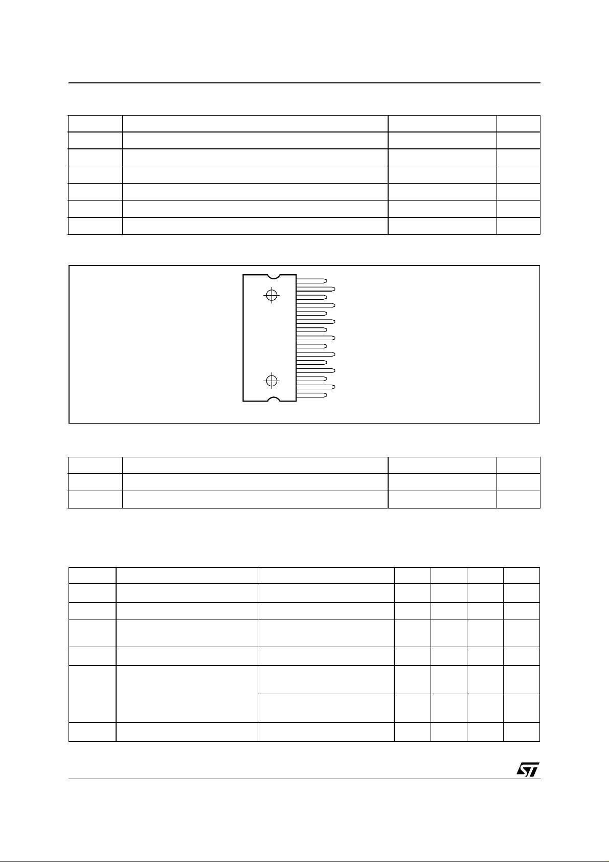
ABSOLUTE MAXIMUM RATINGS
Symbol Parameter Value Unit
V
P
T
T
stg,TJ
V
IN
tot
amb
V
DC Supply Voltage 35 V
S
Maximum Input Voltage 8 Vpp
Total Power Dissipation (T
= 70°C) 16 W
amb
Ambient Operating Temperature (1) 0 to 70 °C
Storage and Junction Temperature -40 to 150 °C
Volume Control DC Voltage 7 V
3
PIN CONNECTION
(top view)
D03AU1505
PW_GND
OUTR
V
S
OUTL
PW_GND
MUTE
STBY
S_GND
SVR
N.C.
INL
VAROUT_L
VOLUME
VAROUT_R
INR
15
14
13
12
11
10
9
8
7
6
5
4
3
2
1
THERMAL DATA
Symbol Parameter Value Unit
R
th j-case
R
th j-amb
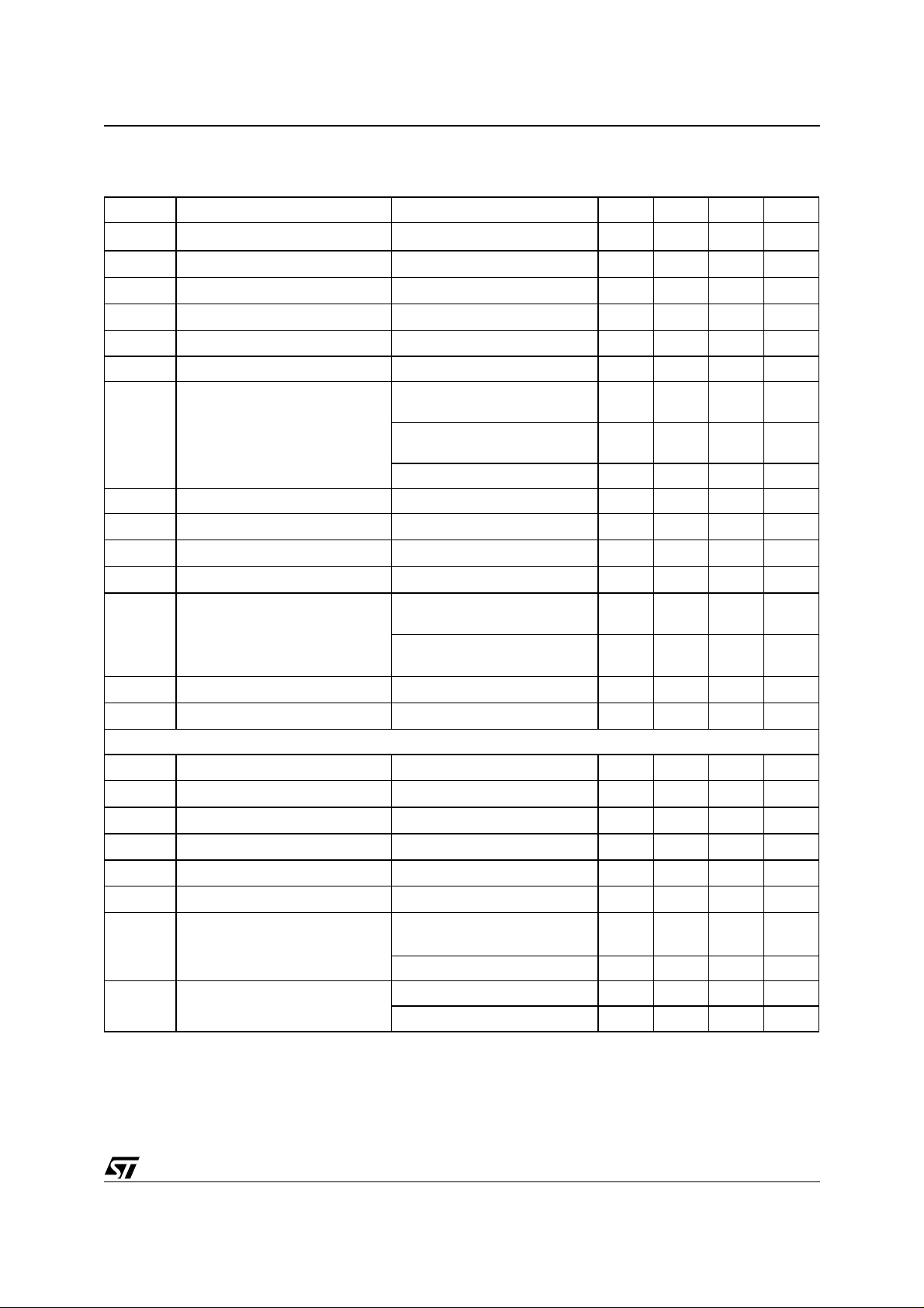
ELECTRICAL CHARACTERISTCS
(Refer to the test circuit R
Symbol Parameter Test Condition Min. Typ. Max. Unit
V
s
I
q
DCV
V
O
P
O
Thermal Resistance junction-case Typ. = 4.5; Max. = 5 °C/W
Thermal Resistance junction-ambient Max. 48 °C/W
= 8Ω, f = 1KHz, Rg = 50Ω, VS = 22V, T
L
Supply Voltage Range 10 32 V
Total Quiescent Current 25 50 mA
Output DC Offset Referred to SVR
os
No Input Signal 200 mV
Potential
Quiescent Output Voltage 11
Output Power THD = 10%; RL = 8Ω;
THD = 1%; RL = 8Ω;
amb
= 25°C)
55.5
4
V
W
2/13
THD
Total Harmonic Distortion
THD = 10%; R
THD = 1%; R
= 4Ω; VS = 12V
L
= 4Ω; VS = 12V
L
Gv = 30dB; PO = 1W; f = 1KHz
2.1
1.0
0.4
W
%
Page 3
TDA7496SA
ELECTRICAL CHARACTERISTCS
(Refer to the test circuit R
= 8Ω, f = 1KHz, Rg = 50Ω, VS = 22V, T
L
(continued)
amb
= 25°C)
Symbol Parameter Test Condition Min. Typ. Max. Unit
I
peak
V
G
G
VLine
A
Min VOL
Output Peak Current (internally limited) 1.0 1.3 A
Input Signal 2.8 Vrms
IN
Closed Loop Gain V
V
Monitor Out Gain V
Attenuation at Minimum Volume V
>4.5V 28.5 30 31.5 dB
Ol Ctrl
>4.5V; Zload >30KΩ -1.5 0 1.5 dB
Ol Ctrl
<0.5V 80 dB
Ol Ctrl
BW 0.6 MHz
e
Total Output Noise f = 20Hz to 22KHz
N
500 800 µV
PLAY, max volume
f = 20Hz to 22KHz
100 250 µV
PLAY, max attenuation
f = 20Hz to 22KHz MUTE 60 150 µV
SR Slew Rate 5 8
R
Input Resistance 22.5 30 KΩ
i
R
Var Out
R
L Var Out
SVR Supply Voltage Rejection f = 1KHz; max volume
T
T
Variable Output Resistance 30 100 Ω
Variable Output Load 2 KΩ
35 39 dB
C
= 470µF; V
SVR
f = 1KHz; max attenuation
= 470µF; V
C
SVR
Thermal Muting 150 °C
M
Thermal Shut-down 160 °C
S
= 1Vrms
RIP
= 1Vrms
RIP
55 65 dB
MUTE & INPUT SELECTION FUNCTIONS
V
ST-ON
V
ST-OFF
V
MUTEON
V
MUTEOFF
A
MUTE
I
qST-BY
I
stbyBIAS
Stand-by ON Threshold 3.5 V
Stand-by OFF Threshold 1.5 V
Mute ON threshold 3.5 V
Mute OFF threshold 1.5 V
Mute Attenuation 50 65 dB
Quiescent Current @ Stand-by 0.6 1 mA
Stand-by bias current Stand by ON: V
V
= 5V
mute
ST-BY
= 5V;
80 µA
Play or Mute -20 -5 µA
I
muteBIAS
Mute Bias Current Mute 1 5 µA
Play 0.2 2 µA
V/µs
3/13
Page 4
TDA7496SA
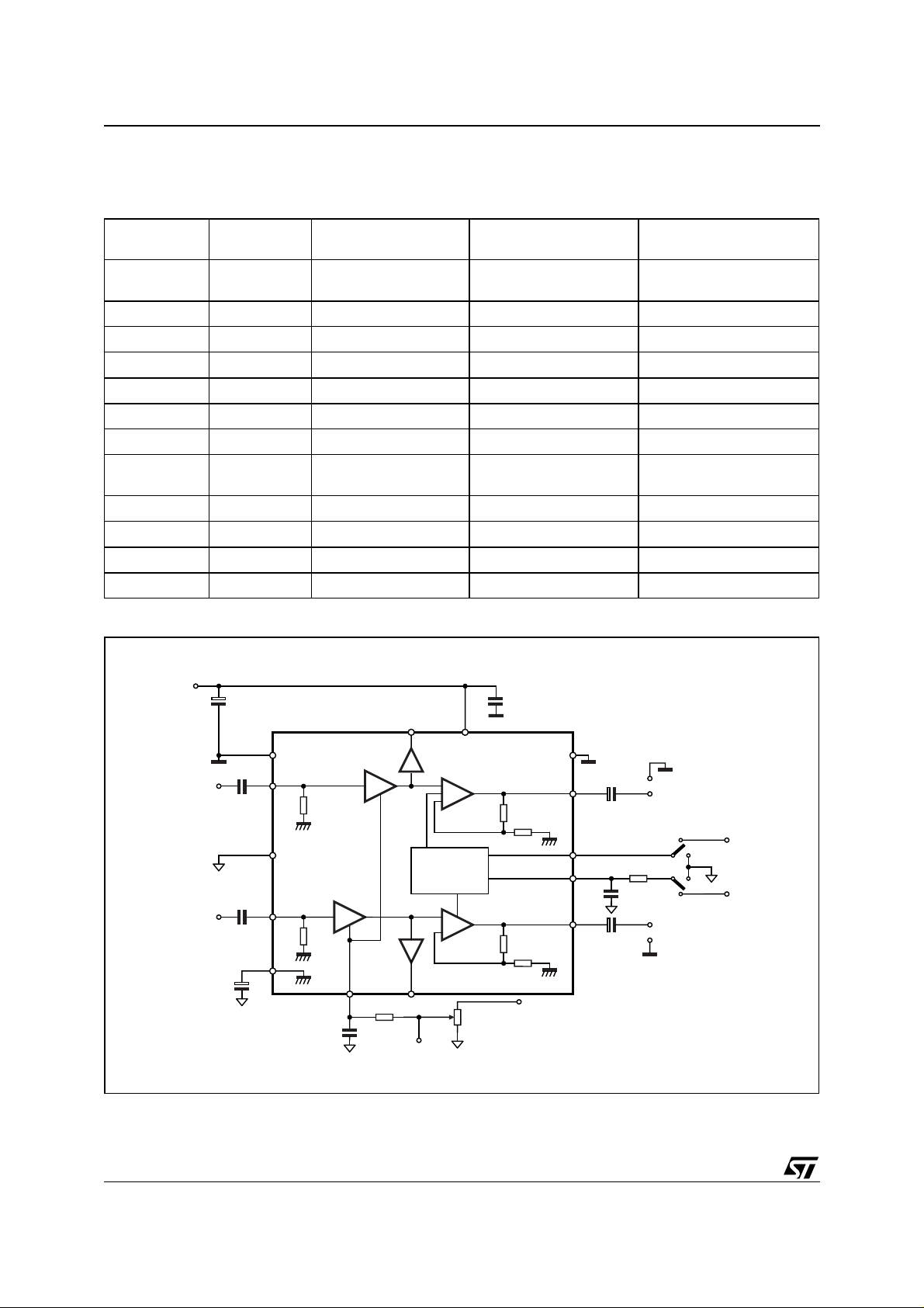
APPLICATION SUGGESTIONS
The recommended values of the external components are those shown on the application circuit of figure 1.
Different values can be used, the following table can help the designer.
COMPONENT
SUGGESTION
VALUE
PURPOSE
R1 300K Volume Control Circuit Larger volume regulation
R2 10K Mute time constant Larger mute on/off time Smaller mute on/off time
P1 50K Volume Control Circuit
C1 1000µF Supply voltage bypass Danger of oscillation
C2 470nF Input DC decoupling Lower low frequency cutoff Higher low frequency cutoff
C3 470nF Input DC decoupling Lower low frequency cutoff Higher low frequency cutoff
C4 470µF Ripple rejection Better SVR Worse SVR
C5 100nF Volume control time
constant
C6 1000µF Output DC decoupling Lower low frequency cutoff Higher low frequency cutoff
C7 1µF Mute time constant Larger mute on/off time Smaller mute on/off time
C8 1000µF Output DC decoupling Lower low frequency cutoff Higher low frequency cutoff
C9 100nF Supply voltage bypass Danger of oscillation
LARGER THAN
SUGGESTION
time
Larger volume regulation
time
SMALLER THAN
SUGGESTION
Smaller volume regulation
time
Smaller volume regulation
time
Figure 1. Application Circui
+V
S
INR
INL
C4 470µF
C1
1000µF
PW_GND
C2 470nF
S_GND
C3 470nF
SVR 7
11
1
8
5
30K
VOLUME
C5
100nF
VAROUT_R
VOLUME
VOLUME
34
VAROUT_L
R1 300K
TP1
2
13
+
OP AMP
MUTE/STBY
PROTECTIONS
+
-30K
OP AMP
V
VOL
P1
50K
LOG
C9
0.1µF
S
PW_GND
15
+5V
C8 1000µF
14
9
10
C7
1µF
12
C6 1000µF
R2 10K
PW_GND
OUTR
OUTL
PW_GND
D96AU493D
S1 STBY
S2 MUTE
+5V
S_GND
+5V
4/13
Page 5
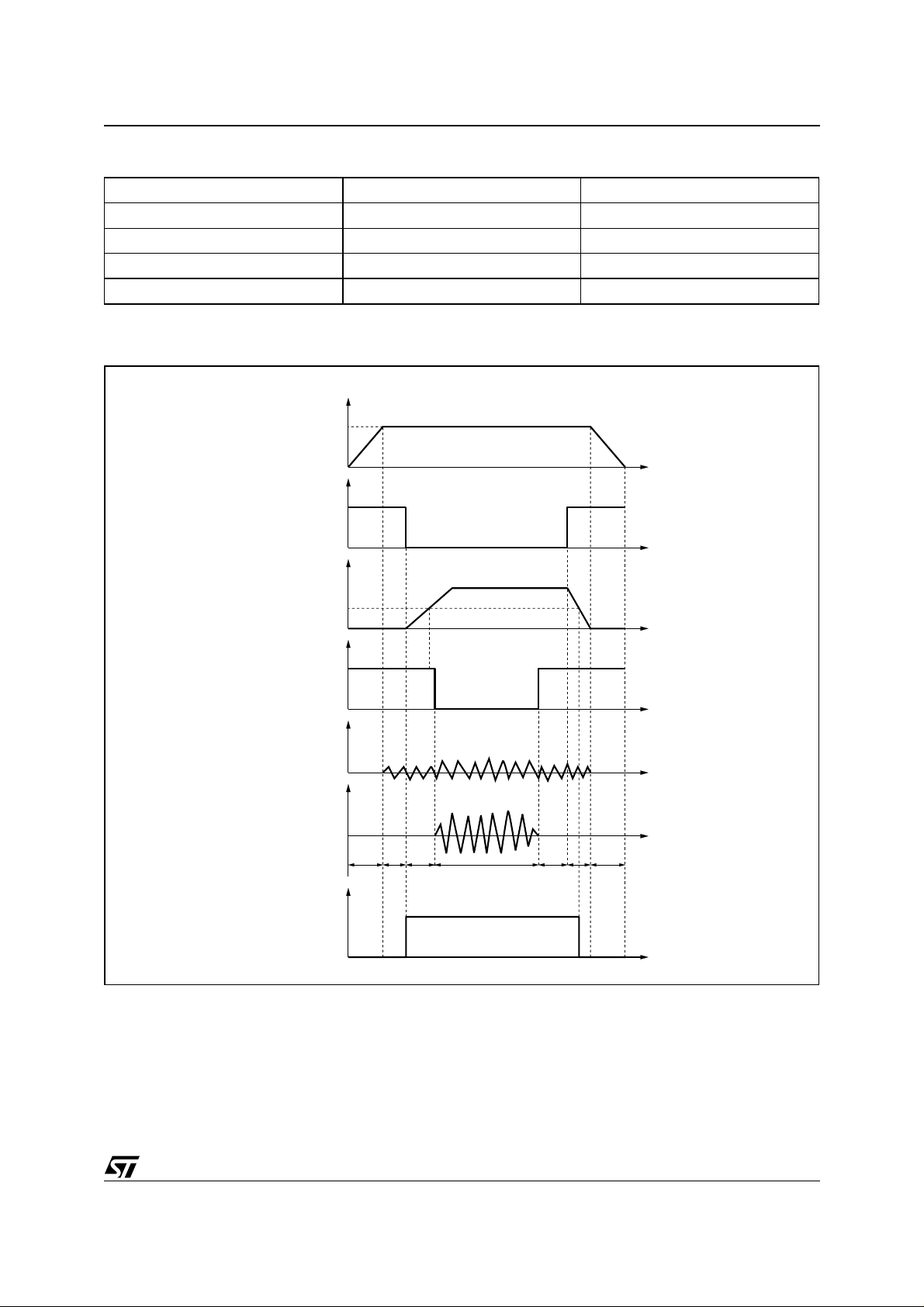
MUTE STAND-BY TRUTH TABLE
MUTE St-BY OPERATING CONDITION
H H STAND-BY
L H STAND-BY
H L MUTE
LLPLAY
Turn ON/OFF Sequences (for optimizing the POP performances)
Figure 1. USING ONLY THE MUTE FUNCTION
VS (V)
ST-BY
pin#9 (V)
5
V
SVR
pin#7(V)
TDA7496SA
2.5V
MUTE
pin#10 (V)
5
INPUT
(mV)
V
OUT
(V)
I
(mA)
Q
D97AU684
OFFSTBY MUTE PLAY STBYOFF MUTE
USING ONLY THE MUTE FUNCTION
To semplify the application, the stand-by pin can be connected directly to Ground. During the ON/OFF transitions is recommended to respect the following conditions:
– At the turn-on the transition mute to mute - play must be made when the SVR pin is higher than 2.5V
– At the turn-of f the TDA 7496A must be brough t to mut e from t he pl ay condi tion when the SVR pin is
higher than 2.5V.
5/13
Page 6
TDA7496SA
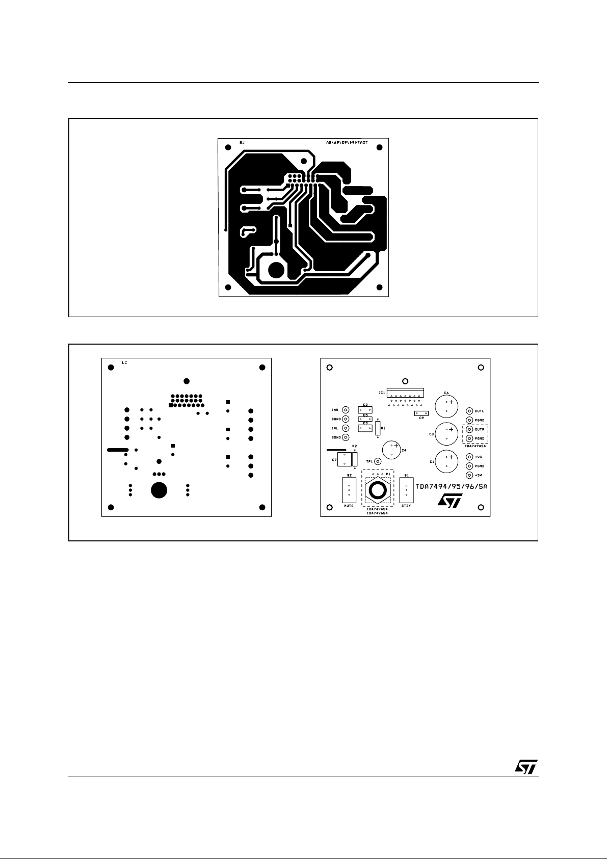
Figure 2. P.C.B. and Component layoutPCB and Component Layout
Figure 3.
6/13
Page 7
TDA7496SA
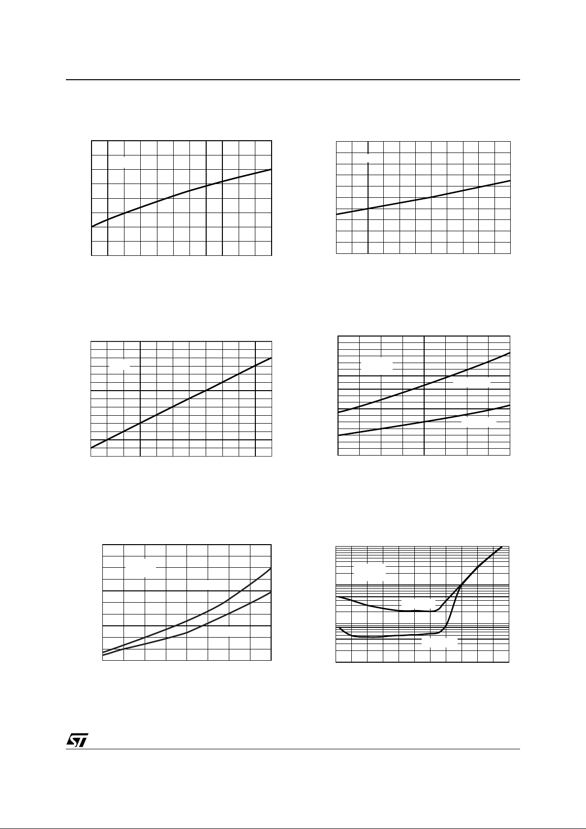
Figure 4. Quiescent Current vs. Supply Voltage
Iq
(mA)
30
28
Vi=0
26
24
22
20
18
16
10 12 14 16 18 20 22 24 26 28 30 32
Supply Voltage (V)
D03AU1494
Figure 5. Output Dc Offset vs. Supply Voltage
Vodc
(V)
16
15
Vi=0
14
13
12
11
10
9
8
7
6
5
4
10 12 14 16 18 20 22 24 26 28 30 32
Supply Voltage (V)
D03AU1495
Figure 7. Output DC Offset vs. Supply Voltage
Vodc-Vsvr
(mV)
280
260
240
220
200
180
160
140
120
100
Vi=0
10 12 14 16 18 20 22 24 26 28 30 32
Supply Voltage (V)
D03AU1496/mod
Figure 8. Out put P ower vs Supply V ol ta ge
Output Power
(W)
3.2
2.8
2.4
2.0
1.6
1.2
0.8
0.4
0
10 10.5 11 11.5 12 12.5 13 13.5 14
Rl=4Ω
F=1KHz
Supply Voltage (V)
D03AU1498
THD=10%
THD=1%
Figure 6. Output Power vs. Supply Voltage
Output Power
(W)
8
7
6
5
4
3
2
1
0
Rl=8Ω
F=1KHz
THD=10%
10 12 14 16 18 20 22 24 26
Supply Voltage (V)
D03AU1497
THD=1%
Figure 9. Disto rti on v s Output Pow er
Distortion
(%)
Vs=22V
Rl=8Ω
1
F=15KHz
0.1
F=1KHz
0.01
0 0.5 1.0 1.5 2.0 2.5 3.0 3.5 4.0 4.5 5.0 5.5
Output Power (W)
D03AU1499
7/13
Page 8
TDA7496SA
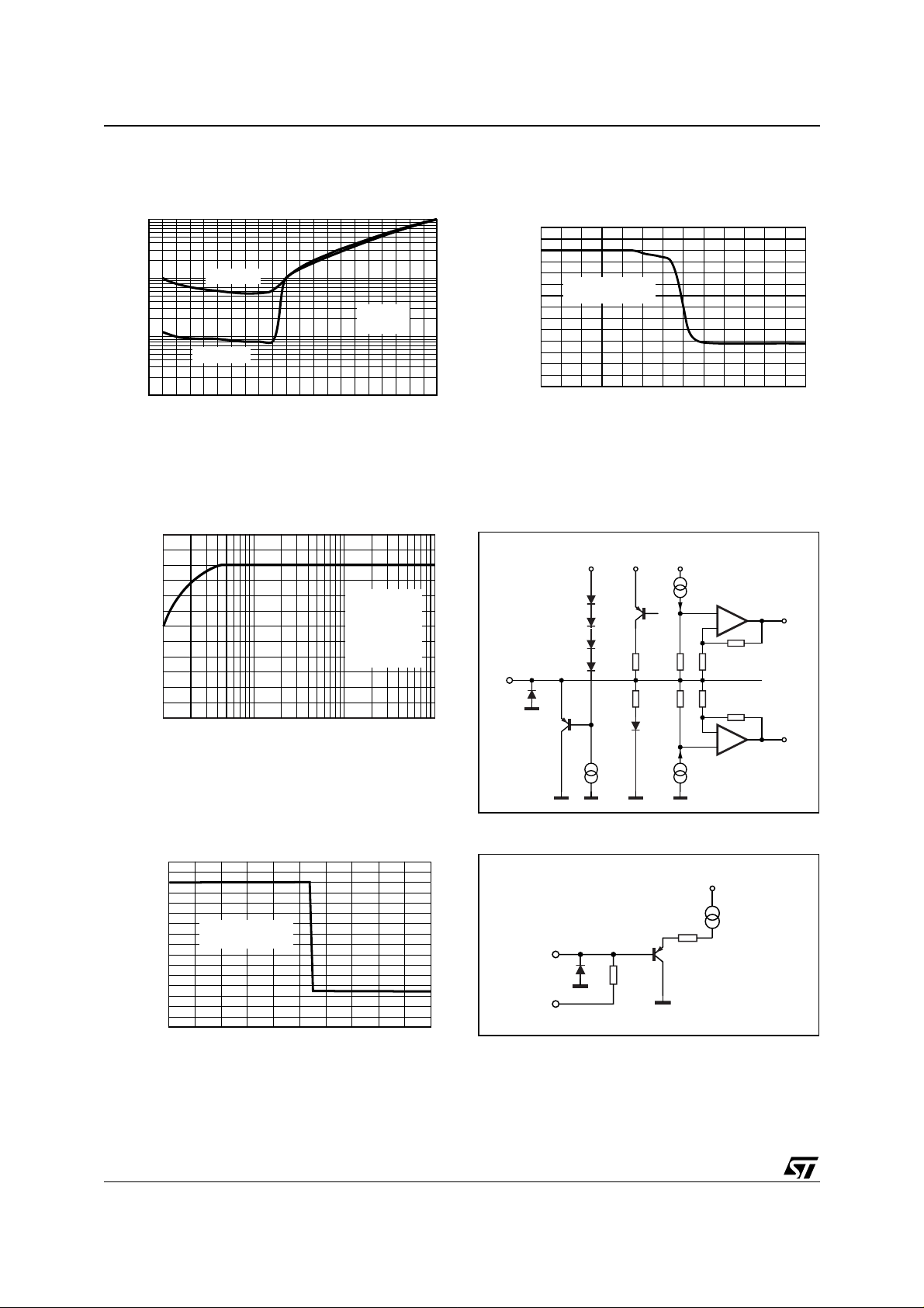
Figure 10. Distortion vs Output Power
Distortion
(%)
1
F=15KHz
0.1
F=1KHz
0.01
0 0.2 0.4 0.6 0.8 1.0 1.2 1.4 1.6 1.8 2.0
Output Power (W)
D03AU1500
Vs=12V
Rl=4Ω
Figure 11. Closed Loop Gain vs. Frequency
Closed loop
Gain
(dB)
30
28
26
24
22
20
0.02 0.2 2 20
Frequency (KHz)
D03AU1501
Rl=8Ω
Pout=0.5W
Cin=470nF
Cout=1000µF
Csvr=470µF
Figure 13. Mute Attenuation vs Vpin 10
Mute Attenuation
(dB)
0
-20
-40
-60
-80
-100
-120
Rl=8Ω
0dB @ Pout=1W
0 0.4 0.8 1.2 1.6 2.0 2.4 2.8 3.2 3.6 4.0 4.4 4.8 5.2
Vpin # 10 (V)
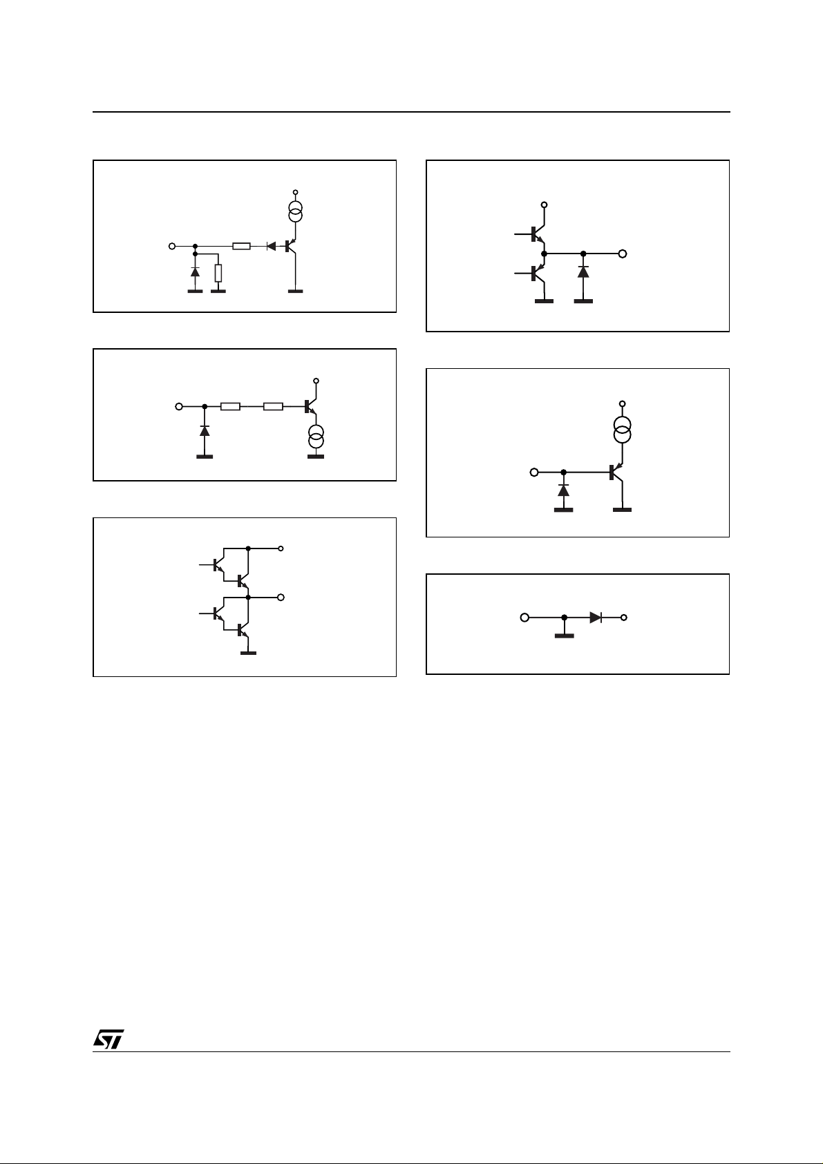
PINS DESCRIPTION
Figure 14. PIN SVR
V
V
S
20K
SVR
20K
V
S
S
+
-
6K
6K
30K
1K
1K
30K
-
+
D03AU1503
OUT L
OUT R
Figure 12. St-By Attenuation vs Vpin 9
St-by Attenuation
(dB)
0
-20
-40
-60
-80
-100
-120
-140
8/13
Rl=8Ω
0dB @ Pout=1W
0 0.5 1.0 1.5 2.0 2.5 3.0 3.5 4.0 4.5 5.0
Vpin # 9 (V)
D03AU1502
Figure 15.
PINS:
INn
SVR
100µA
INL,INR
30K
6K
D97AU589
V
S
D97AU585A
500µA
Page 9
TDA7496SA
3
Figure 17. PIN ST-BY
STBY
200
65K
D97AU594
Figure 18. PIN: MUTE
200MUTE
10K
50µA
D97AU592
Figure 19. PINS: OUT R, OUT L
V
S
Figure 20. PINS: VAROUT-L VAROUT-R
V
S
10µA
V
S
VAROUT-L
D97AU590
Figure 21. PIN: VOLUME
V
S
V
S
10µA
VOL
D97AU591
Figure 22. PINS: PW-GND, S-GND
D97AU588
OUT
GND
D97AU59
V
S
9/13
Page 10
TDA7496SA
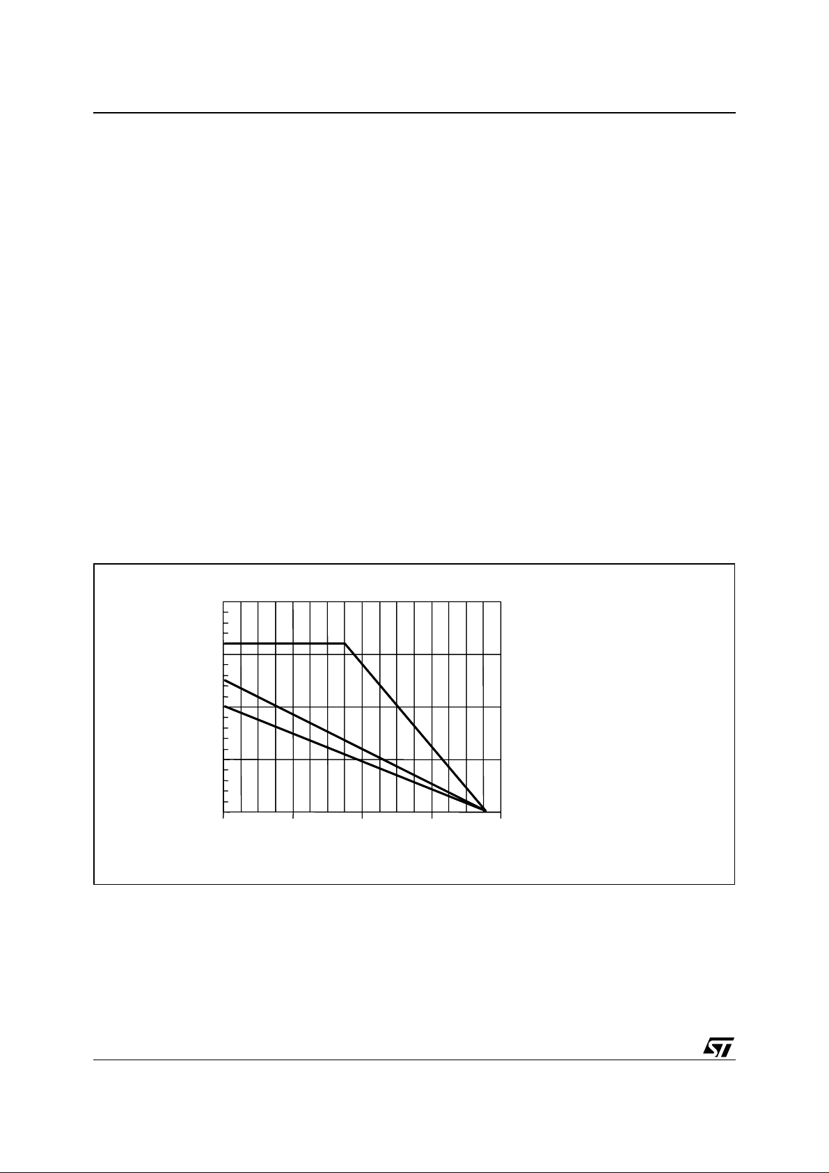
HEAT SINK DIMENSIONING:
In order to avoid the thermal protection intervention, that is placed approximati vely at Tj = 150°C, it is important
the dimensioning of the Heat Sinker R
The parameters that influence the dimensioning are:
– Maximum dissipa ted power for the device (P
– Max thermal resistance Junction to case (R
– Max. ambient temperature T
amb max
– Quiescent current Iq (mA)
Example:
= 22V, R
V
CC
= (N° channels) ·
P
dmax
= 2 · ( 3.0 ) + 0.5 = 6.5 W
P
dmax
(Heat Sinker)
= 8ohm, R
load
R
Th c-a
= 5 °C/W , T
Th j-c
2
V
cc
------------------------------ I
2Π2R
⋅
load
150 T
–
----------------------------------------- R
P
d max
Th
qVcc
amb max
(°C/W).
amb max
⋅+
–
Th j-c
)
dmax
)
Th j-c
= 50°C
150 50–
---------------------- 5.0– 10°C/W===
6.5
In figure 23 is shown the Power derating curve for the device.
Figure 23. Power derating curve
20
20
15
15
(a)
(a)
10
10
Pd (W)
Pd (W)
(c)
5
5
0
0
0 40 80 120 160
0 40 80 120 160
(c)
(b)
(b)
Tamb (°C)
Tamb (°C)
a) Infinite Heatsink
a) Infinite Heatsink
b) 7 °C/ W
b) 7 °C/ W
c) 10 °C/ W
c) 10 °C/ W
10/13
Page 11
TDA7496SA
Clipwatt Assembling Suggestions
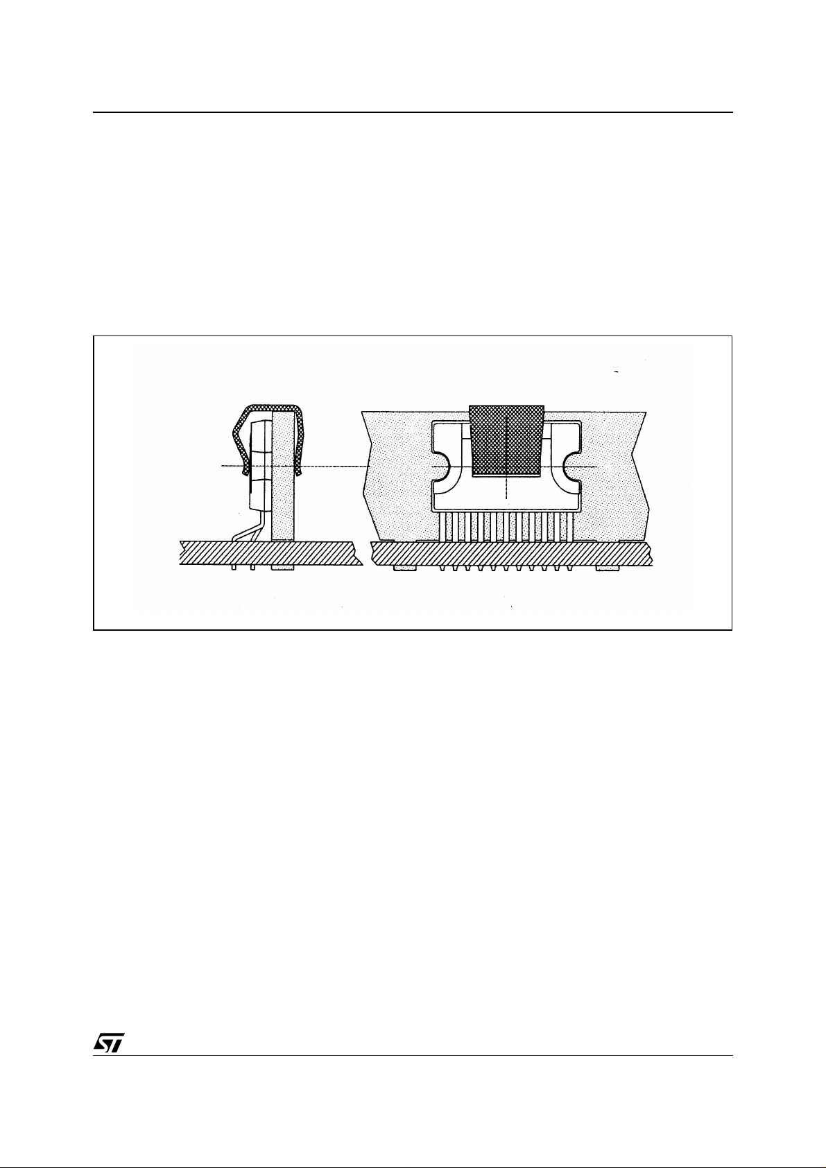
The suggested mounting method of Clipwatt on external heat sink, requires the use of a clip placed as much
as possible in the plastic body center, as indicated in the example of figure 24.
A thermal grease can be used in order to reduce the additio nal thermal resistance of the contact betw een package and heatsink.
A pressing force of 7 - 10 Kg gives a good contact and the clip mus t be designed in order to avoid a maxi mum
contact pressure of 15 Kg/mm2 between it and the plastic body case.
As example , if a 15Kg force is applied by the clip on the package , the clip must have a contact area of 1mm2
at least.
Figure 24. Example of right placement of the clip
11/13
Page 12
TDA7496SA
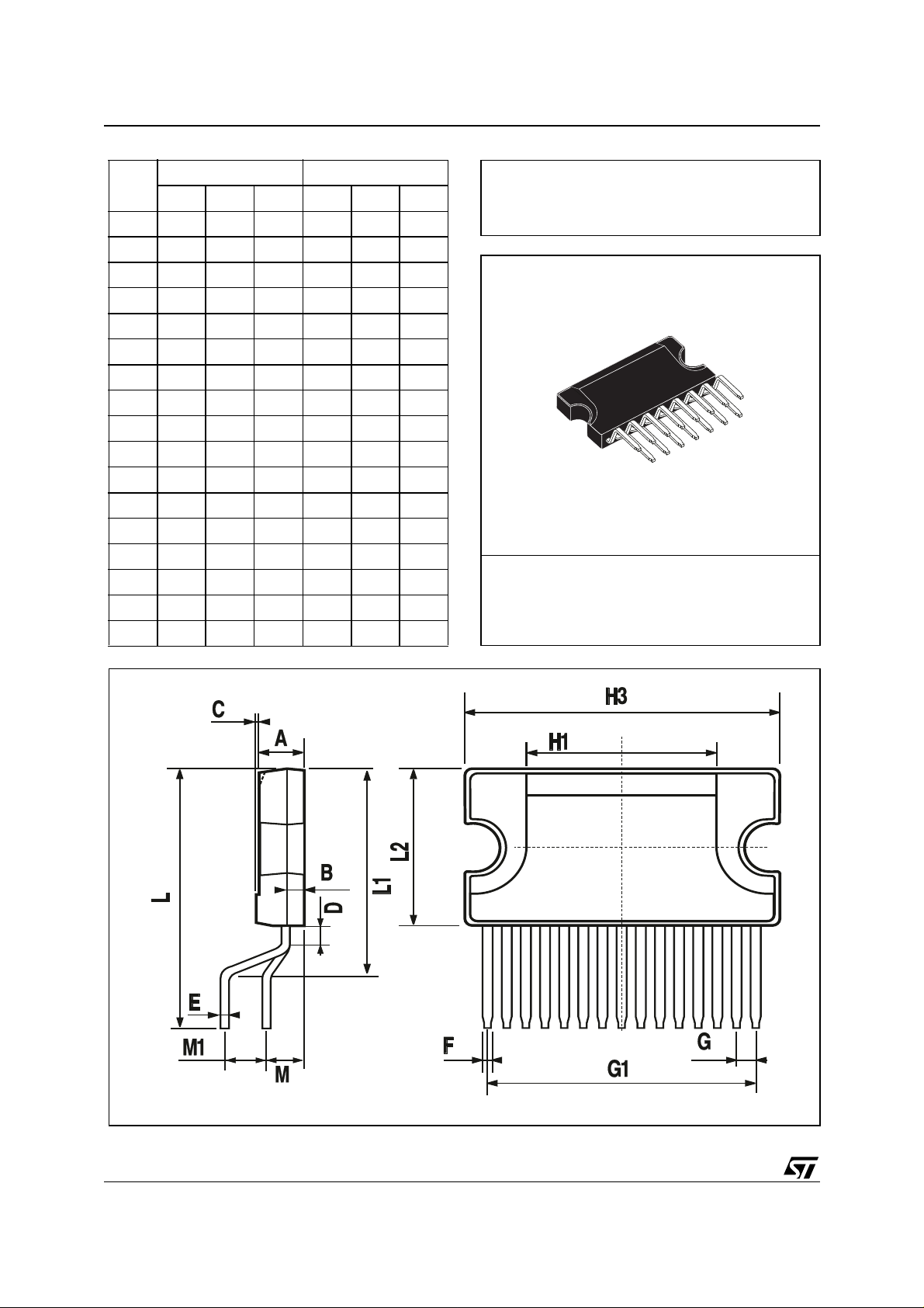
DIM.
mm inch
MIN. TYP . MAX. MIN. TYP. MAX.
A 3.2 0.126
B 1.05 0.041
C 0.15 0.006
D 1.55 0.061
E 0.49 0.55 0.019 0.022
F 0.67 0.73 0.026 0.029
G 1.14 1.27 1.4 0.045 0.050 0.055
G1 17.57 17.78 17.91 0.692 0.700 0.705
H1 12 0.480
H2 18.6 0.732
H3 19.85 0.781
L 17.95 0.707
L1 14.45 0.569
L2 10.7 11 11.2 0.421 0.433 0.441
L3 5.5 0.217
M 2.54 0.100
M1 2.54 0.100
OUTLINE AN D
MECHAN ICAL DATA
Weight:
1.92gr
Clipwatt15
12/13
0044538
Page 13

TDA7496SA
Information furnished is believed to be accurate and reliable. However, STMicroelectronics assumes no responsibility for the consequences
of use of such information nor for any infringement of patents or other rights of third parties which may result from its use. No license is granted
by implic ation or otherwise under any patent or patent r i ght s of STMi croelectr oni cs. Spec i fications mentioned i n this publication are subject
to change without notice. This publication supersedes and replaces all information previously supplied. STMicroelectronics product s are not
authorized for use as cri tical comp onents in lif e support devi ces or systems without express written approva l of STMicroel ectronics.
The ST logo is a registered trademark of STMicroelectr oni cs.
All other n am es are the property of th ei r respectiv e owners
© 2003 STMi croelectronics - All rights reserved
Australi a - B elgium - Brazil - Canada - China - C zech Republi c - Finland - F rance - Germ any - Hong Kong - India - Is rael - Italy - Japan -
Malaysia - Malta - Morocco - Singapore - Spain - Sweden - Switzerland - United Kingdom - United States
STMicroelectronics GROUP OF COMPANIES
www.st.com
13/13
 Loading...