

TDA7572
200W mono bridge PWM amplifier with built-in step-up converter
Preliminary Data
Features
■ Input stage and gain compressor
■ Over-modulation protection and current limiting
■ Modulator
■ DAC
■ Step-up
■ Mode control
■ Diagnostics / safety
■ Power control
Description
TDA7572 is a highly integrated, highly versatile,
semi-custom IC switch mode audio amplifier. It
integrates audio signal processing and power
amplification tailored for standalone remote bass
box applications, while providing versatility for full
bandwidth operation in either automotive or
consumer audio environments. It's configured as
one full bridge channel, using two clocked PWM
modulators driving external, complementary
FET's.
Broad operating voltage is supported, allowing
operation from both 14V and 42V automotive
power buses, as well as from split supplies for
consumer electronics use.
A current mode control boost converter controller
is provided to allow high power operation in a 14V
environment. Turn-on and turn-off transients are
minimized by soft muting/unmuting and careful
control of offsets within the IC.
Digital Audio input is supported by an integrated
one channel DAC. Sophisticated diagnostics and
protection provide fault reporting via I
power shutdown for safety related faults.
TDA7572 is packaged in a HiQUAD-64 package.
HiQUAD-64
2
C and
Table 1. Device summary
Order code Package Packing
TDA7572 HiQUAD-64 Tray
September 2007 Rev 1 1/64
This is preliminary information on a new product now in development or undergoing evaluation. Details are subject to
change without notice.
www.st.com
1

Contents TDA7572
Contents
1 Detailed features . . . . . . . . . . . . . . . . . . . . . . . . . . . . . . . . . . . . . . . . . . . . 7
2 Interface description . . . . . . . . . . . . . . . . . . . . . . . . . . . . . . . . . . . . . . . . . 8
3 Pins description . . . . . . . . . . . . . . . . . . . . . . . . . . . . . . . . . . . . . . . . . . . . 9
4 Electrical specifications . . . . . . . . . . . . . . . . . . . . . . . . . . . . . . . . . . . . . 15
4.1 Absolute maximum ratings . . . . . . . . . . . . . . . . . . . . . . . . . . . . . . . . . . . . 15
4.2 Thermal data . . . . . . . . . . . . . . . . . . . . . . . . . . . . . . . . . . . . . . . . . . . . . . 15
4.3 Electrical characteristics . . . . . . . . . . . . . . . . . . . . . . . . . . . . . . . . . . . . . . 15
4.3.1 Operating voltage and current . . . . . . . . . . . . . . . . . . . . . . . . . . . . . . . . 15
4.3.2 Under voltage lockout . . . . . . . . . . . . . . . . . . . . . . . . . . . . . . . . . . . . . . 16
4.3.3 Input stage . . . . . . . . . . . . . . . . . . . . . . . . . . . . . . . . . . . . . . . . . . . . . . . 18
4.3.4 Oscillator . . . . . . . . . . . . . . . . . . . . . . . . . . . . . . . . . . . . . . . . . . . . . . . . 21
4.3.5 Modulator . . . . . . . . . . . . . . . . . . . . . . . . . . . . . . . . . . . . . . . . . . . . . . . . 22
4.3.6 Gate drive and output stage control . . . . . . . . . . . . . . . . . . . . . . . . . . . . 22
4.3.7 Diagnostics . . . . . . . . . . . . . . . . . . . . . . . . . . . . . . . . . . . . . . . . . . . . . . 23
4.4 Voltage booster . . . . . . . . . . . . . . . . . . . . . . . . . . . . . . . . . . . . . . . . . . . . 24
4.4.1 Digital to analog converter . . . . . . . . . . . . . . . . . . . . . . . . . . . . . . . . . . . 25
4.4.2 I/O pin characteristics . . . . . . . . . . . . . . . . . . . . . . . . . . . . . . . . . . . . . . 26
4.4.3 Op. amp. cells . . . . . . . . . . . . . . . . . . . . . . . . . . . . . . . . . . . . . . . . . . . . 26
4.4.4 Shunt . . . . . . . . . . . . . . . . . . . . . . . . . . . . . . . . . . . . . . . . . . . . . . . . . . . 26
4.4.5 Application information . . . . . . . . . . . . . . . . . . . . . . . . . . . . . . . . . . . . . 27
5I
2
C and mode control . . . . . . . . . . . . . . . . . . . . . . . . . . . . . . . . . . . . . . . 28
5.1 Input control register . . . . . . . . . . . . . . . . . . . . . . . . . . . . . . . . . . . . . . . . . 31
5.2 Faults 1 register . . . . . . . . . . . . . . . . . . . . . . . . . . . . . . . . . . . . . . . . . . . . 32
5.3 Faults 2 register . . . . . . . . . . . . . . . . . . . . . . . . . . . . . . . . . . . . . . . . . . . . 33
5.4 Control register . . . . . . . . . . . . . . . . . . . . . . . . . . . . . . . . . . . . . . . . . . . . . 34
5.5 Modulator register . . . . . . . . . . . . . . . . . . . . . . . . . . . . . . . . . . . . . . . . . . 35
5.6 Testing register . . . . . . . . . . . . . . . . . . . . . . . . . . . . . . . . . . . . . . . . . . . . . 36
6 Input stage and gain compressor . . . . . . . . . . . . . . . . . . . . . . . . . . . . . 37
6.1 Input stage . . . . . . . . . . . . . . . . . . . . . . . . . . . . . . . . . . . . . . . . . . . . . . . . 37
2/64

TDA7572 Contents
6.2 Gain compressor . . . . . . . . . . . . . . . . . . . . . . . . . . . . . . . . . . . . . . . . . . . 37
6.2.1 Setting in I2C bus mode . . . . . . . . . . . . . . . . . . . . . . . . . . . . . . . . . . . . . 38
6.2.2 Soft-mute function, without pre-limiter . . . . . . . . . . . . . . . . . . . . . . . . . . 39
7 Modulator . . . . . . . . . . . . . . . . . . . . . . . . . . . . . . . . . . . . . . . . . . . . . . . . . 41
7.1 FET drive . . . . . . . . . . . . . . . . . . . . . . . . . . . . . . . . . . . . . . . . . . . . . . . . . 42
7.2 ANTI-POP shunt driver . . . . . . . . . . . . . . . . . . . . . . . . . . . . . . . . . . . . . . . 43
8 DAC . . . . . . . . . . . . . . . . . . . . . . . . . . . . . . . . . . . . . . . . . . . . . . . . . . . . . . 44
9 Step-up . . . . . . . . . . . . . . . . . . . . . . . . . . . . . . . . . . . . . . . . . . . . . . . . . . . 46
10 Diagnostics . . . . . . . . . . . . . . . . . . . . . . . . . . . . . . . . . . . . . . . . . . . . . . . 48
10.1 Faults during operation: . . . . . . . . . . . . . . . . . . . . . . . . . . . . . . . . . . . . . . 48
10.1.1 DC offset across the speaker . . . . . . . . . . . . . . . . . . . . . . . . . . . . . . . . . 48
10.1.2 Die temperature . . . . . . . . . . . . . . . . . . . . . . . . . . . . . . . . . . . . . . . . . . . 49
10.1.3 External temperature . . . . . . . . . . . . . . . . . . . . . . . . . . . . . . . . . . . . . . . 49
10.1.4 Output clipping . . . . . . . . . . . . . . . . . . . . . . . . . . . . . . . . . . . . . . . . . . . . 49
10.1.5 Output over-current . . . . . . . . . . . . . . . . . . . . . . . . . . . . . . . . . . . . . . . . 49
10.1.6 Power supply overcurrent . . . . . . . . . . . . . . . . . . . . . . . . . . . . . . . . . . . 50
10.1.7 Fault handling . . . . . . . . . . . . . . . . . . . . . . . . . . . . . . . . . . . . . . . . . . . . 50
10.1.8 Faults during power-up: . . . . . . . . . . . . . . . . . . . . . . . . . . . . . . . . . . . . . 51
11 Oscillator . . . . . . . . . . . . . . . . . . . . . . . . . . . . . . . . . . . . . . . . . . . . . . . . . 53
12 Under voltage lock out (UVLO) . . . . . . . . . . . . . . . . . . . . . . . . . . . . . . . 54
12.1 VSP-UVLO . . . . . . . . . . . . . . . . . . . . . . . . . . . . . . . . . . . . . . . . . . . . . . . . 54
12.2 V14 - UVLO . . . . . . . . . . . . . . . . . . . . . . . . . . . . . . . . . . . . . . . . . . . . . . . 54
12.3 SVR - UVLO . . . . . . . . . . . . . . . . . . . . . . . . . . . . . . . . . . . . . . . . . . . . . . . 55
13 Start-up procedures, modulator turn-on after a tristate condition. . . 56
13.1 Start-up . . . . . . . . . . . . . . . . . . . . . . . . . . . . . . . . . . . . . . . . . . . . . . . . . . 56
13.2 Tristate . . . . . . . . . . . . . . . . . . . . . . . . . . . . . . . . . . . . . . . . . . . . . . . . . . . 56
14 Applications . . . . . . . . . . . . . . . . . . . . . . . . . . . . . . . . . . . . . . . . . . . . . . . 57
14.1 Single supply . . . . . . . . . . . . . . . . . . . . . . . . . . . . . . . . . . . . . . . . . . . . . . 57
14.2 Split supply . . . . . . . . . . . . . . . . . . . . . . . . . . . . . . . . . . . . . . . . . . . . . . . . 59
3/64

Contents TDA7572
14.3 THD+N step-up on . . . . . . . . . . . . . . . . . . . . . . . . . . . . . . . . . . . . . . . . . . 61
15 Package information . . . . . . . . . . . . . . . . . . . . . . . . . . . . . . . . . . . . . . . . 62
16 Revision history . . . . . . . . . . . . . . . . . . . . . . . . . . . . . . . . . . . . . . . . . . . 63
4/64

TDA7572 List of tables
List of tables
Table 1. Device summary . . . . . . . . . . . . . . . . . . . . . . . . . . . . . . . . . . . . . . . . . . . . . . . . . . . . . . . . . . 1
Table 2. Pin list by argument . . . . . . . . . . . . . . . . . . . . . . . . . . . . . . . . . . . . . . . . . . . . . . . . . . . . . . 10
Table 3. Pin list by pin. . . . . . . . . . . . . . . . . . . . . . . . . . . . . . . . . . . . . . . . . . . . . . . . . . . . . . . . . . . . 12
Table 4. Absolute maximum ratings . . . . . . . . . . . . . . . . . . . . . . . . . . . . . . . . . . . . . . . . . . . . . . . . . 15
Table 5. Thermal data. . . . . . . . . . . . . . . . . . . . . . . . . . . . . . . . . . . . . . . . . . . . . . . . . . . . . . . . . . . . 15
Table 6. Operating voltage and current . . . . . . . . . . . . . . . . . . . . . . . . . . . . . . . . . . . . . . . . . . . . . . 15
Table 7. Under voltage lockout . . . . . . . . . . . . . . . . . . . . . . . . . . . . . . . . . . . . . . . . . . . . . . . . . . . . . 16
Table 8. Input stage . . . . . . . . . . . . . . . . . . . . . . . . . . . . . . . . . . . . . . . . . . . . . . . . . . . . . . . . . . . . . 18
Table 9. Oscillator. . . . . . . . . . . . . . . . . . . . . . . . . . . . . . . . . . . . . . . . . . . . . . . . . . . . . . . . . . . . . . . 21
Table 10. Modulator . . . . . . . . . . . . . . . . . . . . . . . . . . . . . . . . . . . . . . . . . . . . . . . . . . . . . . . . . . . . . . 22
Table 11. Gate drive and output stage control . . . . . . . . . . . . . . . . . . . . . . . . . . . . . . . . . . . . . . . . . . 22
Table 12. Diagnostics . . . . . . . . . . . . . . . . . . . . . . . . . . . . . . . . . . . . . . . . . . . . . . . . . . . . . . . . . . . . . 23
Table 13. Voltage booster. . . . . . . . . . . . . . . . . . . . . . . . . . . . . . . . . . . . . . . . . . . . . . . . . . . . . . . . . . 24
Table 14. Digital to analog converter . . . . . . . . . . . . . . . . . . . . . . . . . . . . . . . . . . . . . . . . . . . . . . . . . 25
Table 15. I/O pin characteristics . . . . . . . . . . . . . . . . . . . . . . . . . . . . . . . . . . . . . . . . . . . . . . . . . . . . . 26
Table 16. Op. amp. cells. . . . . . . . . . . . . . . . . . . . . . . . . . . . . . . . . . . . . . . . . . . . . . . . . . . . . . . . . . . 26
Table 17. Shunt . . . . . . . . . . . . . . . . . . . . . . . . . . . . . . . . . . . . . . . . . . . . . . . . . . . . . . . . . . . . . . . . . 26
Table 18. Analog operating characteristics. . . . . . . . . . . . . . . . . . . . . . . . . . . . . . . . . . . . . . . . . . . . . 27
Table 19. Power-up mode control. . . . . . . . . . . . . . . . . . . . . . . . . . . . . . . . . . . . . . . . . . . . . . . . . . . . 28
Table 20. Addresses . . . . . . . . . . . . . . . . . . . . . . . . . . . . . . . . . . . . . . . . . . . . . . . . . . . . . . . . . . . . . . 29
Table 21. I
Table 22. Input control register . . . . . . . . . . . . . . . . . . . . . . . . . . . . . . . . . . . . . . . . . . . . . . . . . . . . . . 31
Table 23. Faults 1 register . . . . . . . . . . . . . . . . . . . . . . . . . . . . . . . . . . . . . . . . . . . . . . . . . . . . . . . . . 32
Table 24. Faults 2 register . . . . . . . . . . . . . . . . . . . . . . . . . . . . . . . . . . . . . . . . . . . . . . . . . . . . . . . . . 33
Table 25. Control register . . . . . . . . . . . . . . . . . . . . . . . . . . . . . . . . . . . . . . . . . . . . . . . . . . . . . . . . . . 34
Table 26. Modulator register . . . . . . . . . . . . . . . . . . . . . . . . . . . . . . . . . . . . . . . . . . . . . . . . . . . . . . . . 35
Table 27. Testing register . . . . . . . . . . . . . . . . . . . . . . . . . . . . . . . . . . . . . . . . . . . . . . . . . . . . . . . . . . 36
Table 28. Distortion versus gain step size . . . . . . . . . . . . . . . . . . . . . . . . . . . . . . . . . . . . . . . . . . . . . 38
Table 29. Sets the maximum release rate of the gain compressor. . . . . . . . . . . . . . . . . . . . . . . . . . . 38
Table 30. Sets the maximum attack rate of the gain compressor. . . . . . . . . . . . . . . . . . . . . . . . . . . . 39
Table 31. Attack/release rate and gain compression effort selection . . . . . . . . . . . . . . . . . . . . . . . . . 39
Table 32. PWMClock table . . . . . . . . . . . . . . . . . . . . . . . . . . . . . . . . . . . . . . . . . . . . . . . . . . . . . . . . . 42
Table 33. Fault handling . . . . . . . . . . . . . . . . . . . . . . . . . . . . . . . . . . . . . . . . . . . . . . . . . . . . . . . . . . . 50
Table 34. Document revision history . . . . . . . . . . . . . . . . . . . . . . . . . . . . . . . . . . . . . . . . . . . . . . . . . 63
2
C chip address . . . . . . . . . . . . . . . . . . . . . . . . . . . . . . . . . . . . . . . . . . . . . . . . . . . . . . . . . 29
5/64

List of figures TDA7572
List of figures
Figure 1. Block diagram . . . . . . . . . . . . . . . . . . . . . . . . . . . . . . . . . . . . . . . . . . . . . . . . . . . . . . . . . . . . 8
Figure 2. Pins connection (top view) . . . . . . . . . . . . . . . . . . . . . . . . . . . . . . . . . . . . . . . . . . . . . . . . . . 9
Figure 3. Mute by external command . . . . . . . . . . . . . . . . . . . . . . . . . . . . . . . . . . . . . . . . . . . . . . . . 39
Figure 4. Mute by I
Figure 5. Modulator block diagram . . . . . . . . . . . . . . . . . . . . . . . . . . . . . . . . . . . . . . . . . . . . . . . . . . 41
Figure 6. Current sourced by the shunt pin in NO I
Figure 7. DAC circuit diagram . . . . . . . . . . . . . . . . . . . . . . . . . . . . . . . . . . . . . . . . . . . . . . . . . . . . . . 44
Figure 8. Two interpolator structure diagram . . . . . . . . . . . . . . . . . . . . . . . . . . . . . . . . . . . . . . . . . . . 45
Figure 9. I
Figure 10. Step-up application diagram . . . . . . . . . . . . . . . . . . . . . . . . . . . . . . . . . . . . . . . . . . . . . . . . 46
Figure 11. Threshold of current limiting diagram . . . . . . . . . . . . . . . . . . . . . . . . . . . . . . . . . . . . . . . . . 47
Figure 12. Single supply evaluation board schematic.. . . . . . . . . . . . . . . . . . . . . . . . . . . . . . . . . . . . . 57
Figure 13. Single supply evaluation PCB. . . . . . . . . . . . . . . . . . . . . . . . . . . . . . . . . . . . . . . . . . . . . . . 58
Figure 14. Split supply evaluation board schematic. . . . . . . . . . . . . . . . . . . . . . . . . . . . . . . . . . . . . . . 59
Figure 15. Split supply evaluation PCB . . . . . . . . . . . . . . . . . . . . . . . . . . . . . . . . . . . . . . . . . . . . . . . . 60
Figure 16. THD+N step-up on . . . . . . . . . . . . . . . . . . . . . . . . . . . . . . . . . . . . . . . . . . . . . . . . . . . . . . . 61
Figure 17. HiQUAD-64 mechanical data and package dimensions . . . . . . . . . . . . . . . . . . . . . . . . . . . 62
2
S format diagram . . . . . . . . . . . . . . . . . . . . . . . . . . . . . . . . . . . . . . . . . . . . . . . . . . . . . . . 45
2
C bus command . . . . . . . . . . . . . . . . . . . . . . . . . . . . . . . . . . . . . . . . . . . . . . . . . 40
2
Cbus mode . . . . . . . . . . . . . . . . . . . . . . . . . . . . 43
6/64

TDA7572 Detailed features
1 Detailed features
● Input Stage and Gain Compressor
– Differential, high CMRR, analog input
– Programmable input attenuation/gain to support up to four drive levels
– Noiseless Gain compression of up to 16 dB with programmable attack and decay.
– Compressor controlled by monitoring estimated THD
– Soft mute / un-mute for pop control
● Over-modulation Protection and Current Limiting
– Adaptive pulse injection prevents missing pulses due to over modulation which
maximizes useful output swing.
– Programmable current limiting based on FET VDS
● Modulator
– Optimized for low distortion at low switching frequency (approximation 110KHz)
– Dual Clocked PWM modulators for 3 state switching
– External gain control / internal integrator components
– Controls 4 external FETS with switching optimized for low EMI
– Oscillation frequency selectable by I
– Anti-pop shunt driver
● DAC
– 18bit, mono
2
–I
S inputs 38-48KHz, 96KHz, 192 KHz
– Hybrid architecture, area optimized for Bass
– Full bandwidth supported by off loading the interpolator function
– Synchronization with modulator
● Step-Up
– On board STEP-UP step up converter, synchronized to the modulator frequency
– Drives external NFET switch
– Externally compensated
– Soft start and current limiting
● Mode Control
– Critical modes controllable by mode pins for bus-less operation
2
–I
C provides additional mode control
● Diagnostics / Safety
– Offset, short, open, overcurrent, over temperature
2
–I
C used to report errors, and for configuration control
– Faults pin used to report errors in bus-less environment
– Clipping reported at a separate pin
– Abnormal supply current detection disables input power for fail safe operation
– Output current limiting
– Power control
– Latching control of an external PMOS power switch for safety related faults.
– Power is switched off for safety related faults of abnormal supply current,
excessive internal or external temperature, or persistent output stage over-current
that fails to be controlled by the pulse-by-pulse current limiting method
2
C
7/64
Interface description TDA7572
2 Interface description
I2C bus and mode control pins are use to control operation. Default values of all the
operating modes are deterministic, some of these values are intrinsic to the IC and some
are determined by configurations pins. The configuration pins are read at power-up and
copied into registers, which may later be modified using the I
allows varied operation in an environment where NOI
2
control and override of pin programmed modes when used with I
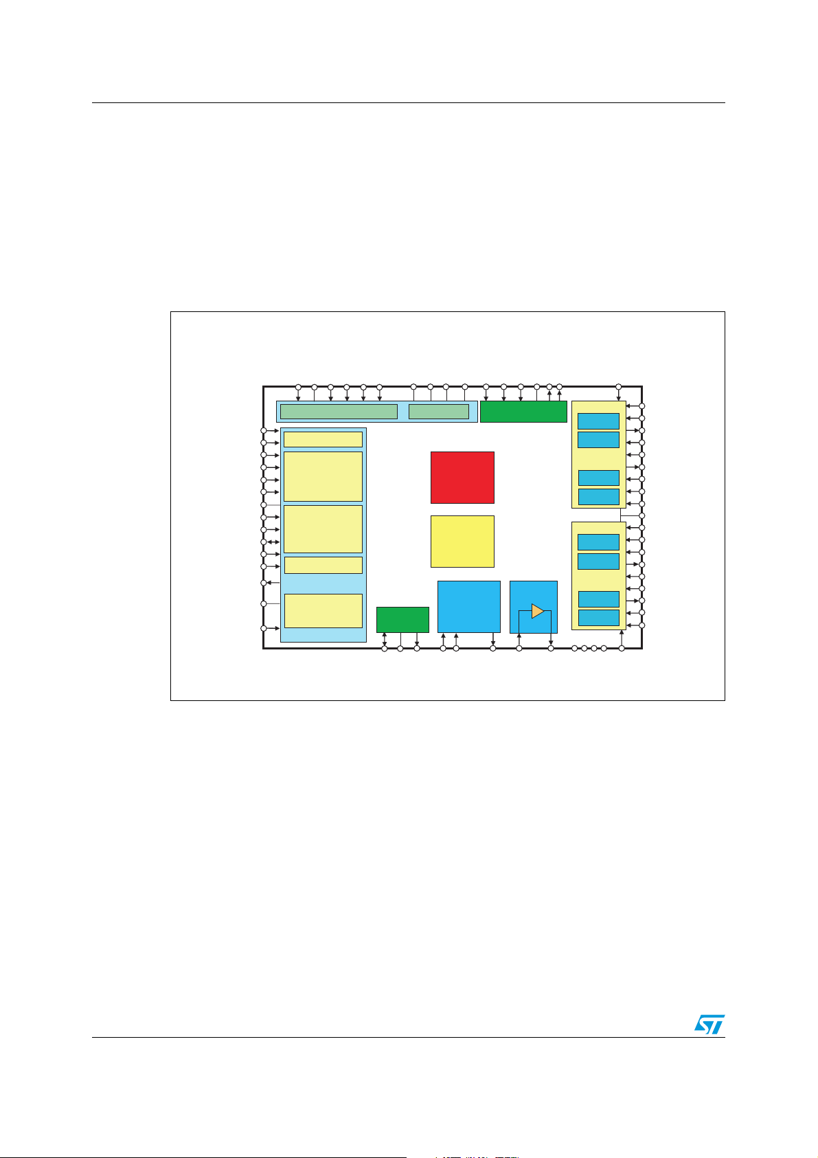
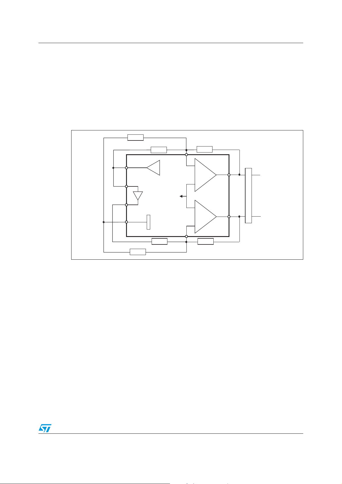
Figure 1. Block diagram
CSense
V14
BSTVSource
BSTGate
BSTVSense
VP2.5
V14Sense
VM2.5
WS / CLIP_L
VDIG
DGND
2
C bus, if one is present. This
C bus is present, while allowing full
SDA / SCR_ENB
2
C.
SCL / InputLevel1
DACM
PLL / InLeve l0
DACP
MOD1
ISSENP
ISSENM
Mode 0
Automute Voltage Setting
Addr 0 / Fault / CLIP_L
Addr1 / CompEnable
Mode 1
Vs/2 or SVR
2
I
C data / attack sel.
2
I
C clock
ShuntDrive
Mute
NTC
TestC
Iset
DC/DC Converter
+Vs current
protection
Mode sel.
and
Mute
I2Cbus
Thermal management
Diagnostics
+
clipdet
Controls and Diagnostics
Oscillators
CLKin -out
Regulators
LOGIC
UVLO
Diff -to-S.E.
Compressor
and
Limiter
Channel 1
INP
INM
OscOut
DITH -sel
AOUT
DAC
-1
InvIn
PWM Channel 1
Pulse Inj.
Integrator
Drivers
Prot. & supply
PWM Channel 2
Pulse Inj.
Integrator
Drivers
Protections
VSM1,2,3,4
InvOut
LSD1SourceSensing
LSD1GateDrive
LSD1GateSensing
HB1OutFilter
HB1Out
ILimit threshold
HSD1GateSensing
HSD1GateDrive
HSD1SourceSensing
VSP_Pow1
HSD2SourceSensing
HSD2GateDrive
HSD2GateSensing
VSP_Pow2
HB2Out
LSD2OutFilter
LSD2GateSensing
LSD2GateDrive
LSD2SourceSensing
MOD2
AC00014
8/64

TDA7572 Pins description
3 Pins description
Figure 2. Pins connection (top view)
Iset
TestC
LSD2SS
LSD2GD
LSD2GS
HB2OutFilt
HB2Out
HSD2GS
HSD2GD
HSD2SS
VSP_POW2
VSP_POW1
HSD1SS
HSD1GD
HSD1GS
HB1Out
HB1OutFilt
LSD1GS
LSD1GD
LSD1SS
I2CLK
IlimitThresh
63
64
1
2
3
4
5
6
7
8
9
10
12
13
14
15
16
17
18
19
20
21 22 23 24 25
VSM4
ADDR1/CompEnable
ADDR0/Fault/Clip_L
I2CDATA/AttackSel
59
60
61
62
26
MUTE_L
AutoMuteVSetting
Mode0
VSM3
58
57 56 55 54 53
271128 29 30 31 32
Mode1
VP2.5
52
51
50
49
48
47
46
45
44
43
42
41
40
39
38
37
36
35
34
33
SVR
VM2.5
VDIG
DGND
NTC
SCL/InLevel1
WS/Clip_L
SDA/SCR_ENB
PLL/InLevel10
ShuntDriver
DITH
CLKIN/Out
OscOut
MOD2
MOD1
InvOut
InvIn
AOUT
INP
INM
BSTGate
BSTSource
CSense
V14Sense
V14
VSM2
AC00013
DAC2
VSM1
BSTVSense
ISSENM
ISSENP
DAC1
9/64

Pins description TDA7572
Table 2. Pin list by argument
Pin # Pin name Description
On/Off Circuitry
11 VSP_POW2
Positive supply power for low power, non gate-drive functions with a separate
bonding to power the gate drive of modulator two
53 VP2.5 +2.5V analog supply output
51 VM2.5 -2.5 V analog supply output
50 VDIG 5V logic supply decoupling
49 DGND Digital gnd
52 SVR Vs/2 analog reference filter capacitor. Reference for input stage.
55 Mode0 Mode control bit0, selects standby/normal/ I2C/diagnostic operation
2
54 Mode1 Mode control bit1, selects standby/normal/ I
C/diagnostic operation
57 MUTE_L Mute input and / or timing cap, assertion level low
56 AutoMuteVSetting Auto-mute Voltage Setting
Input/ Gain Compressor
34 INP Non inverting audio input
33 INM Inverting audio input
35 AOUT Compressed Audio Output
Input Stage gain selection – see PLL pin in DAC Section 8
Compressor attack/decay select – see I2C data pin in DAC Section 8
Inverter
36 InvIn Inverter input
37 InvOut Inverter Output
Modulator
64 IlimitThresh Output stage Current Limiting trip voltage set point
32 LVLSFT Gain program pin for SVR to HVCC level shifting
38 MOD1 Modulator1 Inverting / Summing node
20 LSD1SS Lowside1 Source Sensing
19 LSD1GD Lowside1 Gate Drive
18 LSD1GS Lowside1 Gate sense
17 HB1OutFilt Half bridge1 post-LC filter – for diagnostics
16 HB1Out Half-bridge1 output, HSD 1 drain sense, LSD1 Drain Sense
15 HSD1GS Highside1 Gate sense
14 HSD1GD Highside1 Gate Drive
13 HSD1SS Highside1 Source sense
12 VSP_POW1 Positive supply voltage connection for gate drive circuitry
10/64
TDA7572 Pins description
Table 2. Pin list by argument (continued)
Pin # Pin name Description
39 MOD2 Modulator2 Inverting / Summing node
10 HSD2SS Highside2 Source sense
9 HSD2GD Highside2 Gate Drive
8 HSD2GS Highside2 Gate sense
7 HB2Out Half-bridge2 output, HSD 1 drain sense, LSD1 Drain Sense
6 HB2OutFilt Half bridge2 post-LC filter – for diagnostics
5 LSD2GS Lowside2 Gate sense
4 LSD2GD Lowside2 Gate Drive
3 LSD2SS Lowside2 Source Sense
27 VSM1
26 VSM2
58 VSM3
Die tab connection to lowest supply voltage – gnd for single ended supplies,
negative supply for split supplies
Die tab connection to lowest supply voltage – gnd for single ended supplies,
negative supply for split supplies
Die tab connection to lowest supply voltage – gnd for single ended supplies,
negative supply for split supplies
59 VSM4
Die tab connection to lowest supply voltage – gnd for single ended supplies,
negative supply for split supplies
43 ShuntDriver Shunt Driver
DC-DC
28 BSTVSense Voltage feedback input for Voltage Booster
22 BSTSource Boost Converter NFET Source
21 BSTGate Boost Converter NFET gate drive
23 CSense
Inverting input for Booster Current Sensing and Digital Test Enable (operating
when is more then about 3V under the V14 pin level)
24 V14Sense Non-inverting input for Booster Current Sensing
25 V14 Power for Boost converter gate drive and Output LSD’s
Oscillator
41 CLKIN/Out Clock input
42 DITH Dither capacitor
40 OscOut Oscillator output
Diagnostics / Bus
2
I
62
CDATA/AttackSel
63 I
2
CLK I2C Clock
I2C data (I2C mode)
Compressor aggressiveness selection (non-bus mode)
11/64
Pins description TDA7572
Table 2. Pin list by argument (continued)
Pin # Pin name Description
2
I
C address set (I2C mode)
61 ADDR0/Fault/Clip_L
60 ADDR1/CompEnable
48 NTC Connection for NTC thermistor
2 TestC Test cap used to generate the slow current pulses
1 ISet Program pin for current level used in Short/Open test
30 ISSENP Supply non-inverting current sense
29 ISSENM Supply inverting current sense
DAC
46 WS / Clip_L I
45 SDA/SCR_ENB I
47 SCL/ InLevel1 I
44 PLL/InLevel0 DAC clock PLL filter/ Input Level selection bit 0 (non-DAC mode)
31 DAC2 DAC output voltage p
Fault output in non bus mode (non-bus mode)
Clipping indicator, assertion level low, (when DAC is enabled)
2
C address set (I2C mode)
I
Compressor Enable/disable (non-bus mode)
2
S Word select / Clipping indicator, assertion level low (non-DAC mode)
2
C serial data / SCR ENABLE (non DAC mode)
2
C serial data bit clock/ Input Level selection bit1 (non-DAC mode)
32 DAC1 DAC output voltage n
Table 3. Pin list by pin
Pin # Pin name Description
1 Iset Program pin for current level used in Short/Open test
2 TestC Test cap used to generate the slow current pulses
3 LSD2SS Lowside2 Source Sense
4 LSD2GD Lowside2 Gate Drive
5 LSD2GS Lowside2 Gate sense
6 HB2OutFilt Half bridge2 post-LC filter – for diagnostics
7 HB2Out Half-bridge2 output, HSD 1 drain sense, LSD1 Drain Sense
8 HSD2GS Highside2 Gate sense
9 HSD2GD Highside2 Gate Drive
10 HSD2SS Highside2 Source sense
11 VSP_POW2
Positive supply power for low power, non gate-drive functions with a separate
bonding to power the gate drive of modulator two
12 VSP_POW1 Positive supply voltage connection for gate drive circuitry
13 HSD1SS Highside1 Source sense
14 HSD1GD Highside1 Gate Drive
15 HSD1GS Highside1 Gate sense
12/64
TDA7572 Pins description
Table 3. Pin list by pin (continued)
Pin # Pin name Description
16 HB1Out Half-bridge1 output, HSD 1 drain sense, LSD1 Drain Sense
17 HB1OutFilt Half bridge1 post-LC filter – for diagnostics
18 LSD1GS Lowside1 Gate sense
19 LSD1GD Lowside1 Gate Drive
20 LSD1SS Lowside1 Source Sensing
21 BSTGate Boost Converter NFET gate drive
22 BSTSource Boost Converter NFET Source
23 CSense
Inverting input for Booster Current Sensing and Digital Test Enable (operating
when is more then about 3V under the V14 pin level)
24 V14Sense Non-inverting input for Booster Current Sensing
25 V14 Power for Boost converter gate drive and Output LSD’s
26 VSM2
27 VSM1
Die tab connection to lowest supply voltage – gnd for single ended supplies,
negative supply for split supplies
Die tab connection to lowest supply voltage – gnd for single ended supplies,
negative supply for split supplies
28 BSTVSense Voltage feedback input for Voltage Booster
29 ISSENM Supply inverting current sense
30 ISSENP Supply non-inverting current sense
31 DAC2 Half VCC (VSP- VSM)/2 Used for output stage reference.
32 DAC1 Gain program pin for SVR to HVCC level shifting
33 INM Inverting audio input
34 INP Non inverting audio input
35 AOUT Compressed Audio Output
36 InvIn Inverter input
37 InvOut Inverter Output
38 MOD1 Modulator1 Inverting / Summing node
39 MOD2 Modulator2 Inverting / Summing node
40 OscOut Oscillator output
41 CLKIN/Out Clock input
42 DITH Dither capacitor
43 ShuntDriver Shunt Driver
44 PLL/InLevel0 DAC clock PLL filter/ Input Level selection bit 0 (non-DAC mode)
2
45 SDA/SCR_ENB I
46 WS / Clip_L I
47 SCL/ InLevel1 I
C serial data / SCR ENABLE (non DAC mode)
2
S Word select / Clipping indicator, assertion level low (non-DAC mode)
2
C serial data bit clock/ Input Level selection bit1 (non-DAC mode)
48 NTC Connection for NTC thermistor
13/64
Pins description TDA7572
Table 3. Pin list by pin (continued)
Pin # Pin name Description
49 DGND GND logic supply decoupling
50 VDIG 5V logic supply decoupling
51 VM2.5 -2.5 V analog supply output
52 SVR Vs/2 analog reference filter capacitor. Reference for input stage.
53 VP2.5 +2.5 V analog supply output
2
54 Mode1 Mode control bit1, selects standby/normal/I
55 Mode0 Mode control bit0, selects standby/normal/ I
56 AutoMuteVSetting Auto-mute Voltage Setting
57 MUTE_L Mute input and / or timing cap, assertion level low
58 VSM3
59 VSM4
60 ADDR1/CompEnable
61 ADDR0/Fault/Clip_L
Die tab connection to lowest supply voltage – gnd for single ended supplies,
negative supply for split supplies
Die tab connection to lowest supply voltage – gnd for single ended supplies,
negative supply for split supplies
2
C address set (I2C mode)
I
Compressor Enable/disable (non-bus mode)
2
I
C address set (I2C mode)
Fault output in non bus mode (non-bus mode)
Clipping indicator, assertion level low, (when DAC is enabled)
C/diagnostic operation
2
C/diagnostic operation
62 I2CDATA/AttackSel
63 I
2
CLK I2C Clock
I2C data (I2C mode)
Compressor aggressiveness selection (non-bus mode)
64 IlimitThresh Output stage Current Limiting trip voltage setpoint
14/64

TDA7572 Electrical specifications
4 Electrical specifications
4.1 Absolute maximum ratings
Table 4. Absolute maximum ratings
Symbol Parameters Test Conditions Min. Max. Units
V
V
V
T
P
DMAX
SP
peak
DATA
T
Stg
Supply voltage VSM -0.6 VSM +58 V
Peak supply voltage (VS+ - VS-) time ≤ 50ms 68 V
Data pin voltage w.r.t Dgnd VS—0.6 6V V
Junction temperature -40 150 C
J
Storage temperature -55 150 C
Power Dissipation
Any operating condition
For thermal budgeting
2.5 W
4.2 Thermal data
Table 5. Thermal data
Symbol Parameters Value Units
R
Th j-case
Thermal resistance junction to case 3 °C/W
4.3 Electrical characteristics
Unless otherwise specified, all ratings below are for -40°C < TJ < 125°C, VSP = 42V, VSM =
0V and the application circuit of Figure 12. Operation of the IC above this junction
temperature will continue without audible artifacts until thermal shutdown, but these
parameters are not guaranteed to be within the specifications below. F
PWM
=110KHz,
Booster not enabled.
4.3.1 Operating voltage and current
Table 6. Operating voltage and current
Symbol Parameters Test conditions Min. Typ. Max. Units
V
SP42
V
SP14
Operating voltage 42V
automotive range
Operating voltage 14.4V
automotive range
Normal operation without audible
defects required
Single ended supply 42V
configuration, V
SM
=0
Normal operation without audible
defects required
Single ended supply 14V
configuration, V
SM
=0
15/64
30 42 58
9 14.4
V

Electrical specifications TDA7572
Table 6. Operating voltage and current (continued)
Symbol Parameters Test conditions Min. Typ. Max. Units
Normal operation required
V
I
SPLIT
stdby
Operating voltage VSP -
split supply rails
V
SM
Stand-by current
Split supply application
SVR
VSM<V
+4
SVR-4,
configuration,
VSP>V
IC in standby, Mode0, and Mode1
= 42V
low V
s
848 58 V
50 at
= 25°C
T
10 at
μA
T = 85°C
V14 13 20
VSP 15 25
I
tristate
Tristate current
Outputs tristated
Booster not running,
= nominal
F
pwm
V14 10
I
MUTE
Mute mode current MUTE asserted,
VSP 20
4.3.2 Under voltage lockout
Table 7. Under voltage lockout
Symbol Parameters Test conditions Min. Typ. Max. Units
V
LimAM
VSP UVLO
V
AM
VPO-
VPO+
V
V
UC
AutomuteVSetting pin
voltage limit
Auto-mute supply
voltage VSP
Auto-tristate supply
voltage VSP negative
slope
Auto-tristate supply
voltage VSP positive
slope
Auto-tristate supply
U
voltage VSP
Relative maximum value
Voltage limit respect to the SVR pin
Allowed voltage range on Automute
pin
Mute is forced if VSP-VSVR or
VSVR-VSM is less than this value
VautomuteVSetting-V
SVR
=VVSVR
The IC is set in tristate if VSP-VSM
is less than this value
Vautomute VSetting-V
=VVSVR
SVR
The IC is set out from tristate if
VSP-VSM is higher than this value
Vautomute VSetting-V
=VVSVR
SVR
The IC is set in tristate if VSP-VSM
is more than this value
Vautomute VSetting-V
=VVSVR
SVR
0.5 2.1 V
-15%
-15%
-15%
-15%
VVSVR*
7
VVSVR
*12
VVSVR
*13
VVSVR*
48
+15% V
+15% V
+15% V
+15% V
Auto-tristate supply
voltage
VSP
Absolute maximum
The IC is set in tristate if VSP-VSM
is higher than this value
60 63 66 V
value
mA
mA
16/64
TDA7572 Electrical specifications
Table 7. Under voltage lockout (continued)
Symbol Parameters Test conditions Min. Typ. Max. Units
V14 – UVLO
Auto-tristate supply
V14-
voltage V14 negative
slope
Auto-tristate supply
V14+
voltage V14 positive
slope
V14h
Auto-tristate 14V voltage
hysteresis
V14su Step-up tristate
Auto-mute supply
V14mute-
voltage V14 negative
slope
Auto-mute supply
V14mute+
voltage V14 positive
slope
SVR – UVLO
Vsvr-
Vsvr+
Auto-tristate SVR
voltage negative slope
Auto-tristate SVR
voltage positive slope
Auto-tristate SVR
VPOH
Voltage
hysteresis
The IC is kept in tristate if 14V VSM become lower than this value
The IC is goes out from tristate if
14V-VSM become higher than this
value
Comparator hysteresis for autotristate threshold
The step-up is in tristate when
voltage lower than this threshold
The IC goes in mute if 14V-VSM
become lower than this value
The IC goes in play if 14V-VSM
become higher than this value
The IC is kept in tristate if VSvr VSM become less than this value
Vautomute VSetting-V
=VVSVR
SVR
The IC is goes out from tristate if
Vvr - VSM become higher than this
value
Vautomute VSetting-V
=VVSVR
SVR
Comparator hysteresis for autotristate threshold
Vautomute VSetting-V
=VVSVR
SVR
5.5 7 V
6.5 8 V
0.8
V
58V
V14-
+
0.7V
V14V+
+
40mV
V14-
+
1.2V
V14V+
+
170mV
V
5
-15%
x
+15% V
VVSVR
6
-15%
x
+15% V
VVSVR
0.40
X
VVSVR
1.2V
X
VVSVR
V
17/64
Electrical specifications TDA7572
4.3.3 Input stage
Table 8. Input stage
Symbol Parameters Test conditions Min. Typ. Max. Units
Input diff. amp./ gain attenuator
R
IN,
No
compress
INLEVEL1=0, INLEVEL0=0 -30% 20 +30%
INLEVEL1=0, INLEVEL0=1 -30% 12 +30%
INLEVEL1=1, INLEVEL0=0 -30% 22 +30%
ion
INLEVEL1=1, INLEVEL0=1 -30% 12 +30%
Input resistance
INLEVEL1=0, INLEVEL0=0 -30% 15.6 +30%
R
max
IN
INLEVEL1=0, INLEVEL0=1 -30% 12 +30%
compress
ion
INLEVEL1=1, INLEVEL0=0 -30% 16 +30%
INLEVEL1=1, INLEVEL0=1 -30% 12 +30%
INLEVEL1=0, INLEVEL0=0 2 V
INLEVEL1=0, INLEVEL0=1 7 V
INLEVEL1=1, INLEVEL0=0 2.6 V
INLEVEL1=1, INLEVEL0=1 9.5 V
INLEVEL1=1,INLEVEL0=1
Not tested in production
(V
AOUT-VSVR
) / (VInP-VinM)
INLEVEL1=0, INLEVEL0=0,
-10 +10
-4 -3 -2 dB
V
A
InMax
IN_0
Input clipping level
Voltage level of the input
that trespassed cause
clipping in the preamplifier
no compression
KΩ
RMS
RMS
RMS
RMS
A
IN_2
A
IN_1
A
IN_3
V
outH
V
outL
AOUT
Input stage gain
AOUT output voltage swing
AOUT output swing
THD
THD
(V
- V
AOUT
) / (VInP-VinM)
SVR
INLEVEL1=0, INLEVEL0=1,
no compression
(V
- V
AOUT
) / (VInP-VinM)
SVR
INLEVEL1=1, INLEVEL0=0
no compression
(V
- V
AOUT
) / (VInP-VinM)
SVR
INLEVEL1=1, INLEVEL0=1,
no compression
With respect to SVR, 10K loading
to a buffered version of SVR
With respect to SVR, 10K loading
to a buffered version of SVR
Vin=1Vrms, f=20-20KHz,
INLEVEL1=0, INLEVEL0=0,
no compression
-15 -14 -13 dB
-6.3 -5.3 -4.3 dB
-17.6 -16.6 -15.6 dB
2V
-2 V
0.01 0.05 %
18/64
TDA7572 Electrical specifications
Table 8. Input stage
Symbol Parameters Test conditions Min. Typ. Max. Units
Vin=1KHz square wave, 2Vpp,
Output slew rate
INLEVEL1=0, INLEVEL0=0,
no compression
Time to transition from 10% to 90%
8µS
AOUT clip detector
f
-3dB
CMRR
Frequency response
Common Mode Rejection
Ratio
CG Common gain
CG Common gain
CG Common gain
CG Common gain
PSRR
V
offset
Power Supply Rejection,
Vsp supply
Output offset
Eno Noise
Duty cycle of the Clipping signal
TBD %
when there is 5% distortion at the
output of AOUT, f=1KHz,
=10kOhm
R
L
Vin=1Vrms,
INLEVEL1=0, INLEVEL0=0
=1V
V
CM
CMRR= A
@1KHz
RMS
VDIFF/AVCM
INLEVEL1=0, INLEVEL0=0
15 25
20 KHz
47 dB
No compressor
VCM=1V
INLEVEL1=0, INLEVEL0=0
RMS
@1KHz
51 dB
No compressor
V
=1V
CM
INLEVEL1=1, INLEVEL0=0
RMS
@1KHz
51 dB
No compressor
VCM=1V
INLEVEL1=0, INLEVEL0=1
RMS
@1KHz
51 dB
No compressor
VCM=1V
INLEVEL1=1, INLEVEL0=1
RMS
@1KHz
51 dB
No compressor
freq<10KHz 60 80 dB
V
with respect to SVR
Offset
Rin=100 ohms, Mute state
-4 0 +4 mV
Noise at output of this stage
f = 20-20KHz, R
= 100ohms
input
710µV
A weighting
RMS
Gain compressor
Maximum attenuation
INLEVEL1=0, INLEVEL0=0 -21 -19 -17
INLEVEL1=0, INLEVEL0=1 -30 -28 -26
dB
INLEVEL1=1, INLEVEL0=0 -25 -23 -21
INLEVEL1=1, INLEVEL0=1 -34 -32 -30
19/64

Electrical specifications TDA7572
Table 8. Input stage
Symbol Parameters Test conditions Min. Typ. Max. Units
Mute
0.5+
0.25
0.44+
0.25
dB
0.55+
0.25
0.48+
0.25
Attenuation step size
Gain Change ZC
comparator offset
(in the diff. – S.E. block)
offset
INLEVEL1=0, INLEVEL0=0 0.5-0.25 0.5
INLEVEL1=0, INLEVEL0=1
INLEVEL1=1, INLEVEL0=0
INLEVEL1=1, INLEVEL0=1
0.44-
0.25
0.55-
0.25
0.48-
0.25
0.44
0.55
0.48
Observed at AOUT pin
ZC crossing must be detected
within 50mV of the actual zero
-80 80 mV
crossing,
Gain Change ZC
comparator offset
(in the diff. – S.E. block)
Observed at InvOut pin
ZC crossing must be detected
-220 +220 mV
offset
Mute attenuation
Mute pin voltage = Dgnd
Vin=1Vrms
90 dB
Charge current Mute Pin Voltage(57) = 1.5V -30% 100 +30% µA
Discharge current Mute Pin Voltage(57) = 1.5V -30% 100 +30% µA
Mute threshold
Maximum voltage where we must
be in complete mute
1.5 V
Unmute threshold 2.5 V
Mute to unmute transition
voltage
Vol
IC in mute mode, FastMute=1
Iout=0
Voh IC in unmute, Iout=0
0.2 0.3 0.42 V
Digital
GND +
0.1
DIGITAL-
V
0.1
V
V
Fast mute Resistance
FASTMUTE=1
Vmutepin=1.5Volts
20/64
420 550 680 Ohm

TDA7572 Electrical specifications
4.3.4 Oscillator
Table 9. Oscillator
Symbol Parameters Test conditions Min. Typ. Max. Units
Internal oscillator
PWMCLOCK=[0 1] 100K 120 140K KHz
F
F
PWM_NOM
CLK
Switching frequency
PWMCLOCK=[1 0]
PWMCLOCK=[0 0]
Duty cycle 48 50 52 %
DC
PWM_NOM
*2
F
PWM_NOM
/2
Clock output high value
V
CLK_High
Maximum voltage level
Load = 20Kohm and 100pF
-0.1 V
V
P25
P25
to buffered SVR
Clock output low value
V
CLK_Low
Minimum voltage level
Load = 20Kohm and 100pF
-0.1 V
V
M25
M25
to buffered SVR
V
CLK-P-P
Peak-peak voltage
Load = 20Kohm and 100pF
to SVR
-10% 4.7 +10% V
Dither cap charge current Dither pin voltage= 2.5V -20% 100 +20% µA
Dither cap discharge
current
Peak-peak dither voltage
swing
Dither external clock
determination
Voltage at the dither pin at to
select external clock function
-20% 100 +20% µA
1.4 1.6 1.7 V
VDIG-0.2 V
V
V
No dither
Peak F
increase due
PWM
to dither
Peak F
decrease due
PWM
to dither
Triangular peak value
Voltage at the dither pin at
which no dither will occur
VDGND
+0.2
Cdither=100nF +8 +10 +12 %
Cdither=100nF -8 -10 -12 %
VGND+
1V
VDIG-
1V
21/64
V
Electrical specifications TDA7572
4.3.5 Modulator
Table 10. Modulator
Symbol Parameters Test conditions Min. Typ. Max. Units
Integrator op. amp.
Int_Voff Input offset voltage -2.5 +2.5 mV
Int_ibias Input bias current Guaranteed by design 500 nA
T
Maximum duty cycle Vsp =1 4.4 1.1 µs
off
4.3.6 Gate drive and output stage control
Table 11. Gate drive and output stage control
Symbol Parameters Test conditions Min. Typ. Max. Units
V
OL_LSD
V
OH_LSD
V
OL_HSD
LSG low voltage
LSG high voltage
HSG low voltage
I
sink
I
sink
I
source
I
source
I
sink
I
sink
= 0.5A
= 20mA
= 0.5A
= 20mA
= 0.5A
= 20mA
1.75
0.080
7
9.2
VSP-7
VSP-
9.2
V
V
V
V
OH_HSD
HSG high voltage
HSG low Z drive t
LSG low Z drive t
HSG HiZ sink current V
LSG HiZ source current V
Overcurrent sensing
I
limThresh
Range of I
Vilim
Vilim
Vitrip
Anti-shoo through
PV
PV
GS_ON
GS_OFF
PFET gate voltage that will
block NFET enhancement
PFET gate voltage that will
allow NFET enhancement
delay
delay
lim Trthresh
VSP-
I
source
I
source
= 0.5A
= 20mA
1.75
VSP-
0.080
After a commutation 2 10 µs
After a commutation 2 10 µs
HSG=VSP
LSG=VSM
t>5uS 150 mA
, t>5uS 150 mA
0.3 1.1 V
Engagement of the current limiting
VlimitTreshold=1V w.r.t. VM2p5
Start of cycle by cycle current
limiting
Vlim*
3.0
-15%
Vlim *
6.0
Vlim*
5.0
+15% V
-2.5 V
-3.5 V
V
V
22/64

TDA7572 Electrical specifications
Table 11. Gate drive and output stage control (continued)
Symbol Parameters Test conditions Min. Typ. Max. Units
NV
NV
GS_ON
GS_OFF
NFET gate voltage that will
block PFET enhancement
NFET gate voltage that will
allow PFET enhancement
2.5 V
3.5 V
4.3.7 Diagnostics
Table 12. Diagnostics
Symbol Parameters Test conditions Min. Typ. Max. Units
Turn-on diagnostics/ Power up diagnostics
I
TEST
V
LSSHRT
V
NOP
-15%
Test current for short/open
R
allowed range 5.6 ohm
ISET
set = 56ohm -15% 15 +15%
R
i
Short threshold to lower
supply rail
Normal operation
thresholds
-Vs+2 -Vs+5.5 V
2.45/(3*
Riset)
+15% mA
-Vs +1 V
Short to supply -Vs+8
Shorted load 6mV
Normal load .025 1 V
Open load 2 V
Test charge current -30% 10µA +30% µA
t
TEST
Test time 60 80 100 ms
Permanent Diagnostics
V
offACT
V
offACT
DC offset detected +-3 Volts
DC offset not detected,
normal operation allowed
+-1.2 Volts
Tem peratur e
T
WARN
Chip thermal warning 135 150 165 °C
Chip thermal warning
hysteresis
357
T Chip thermal shutdown 155 160 175 °C
Shutdown hysteresis 3 5 7 °C
External thermal warning -10% V
External thermal warning
hysteresis
Vdig*0.0
30
*.4 +10% V
DIG
Vdig*0.
044
V
23/64

Electrical specifications TDA7572
Table 12. Diagnostics (continued)
Symbol Parameters Test conditions Min. Typ. Max. Units
Supply I
Ext thermal shut down -15% V
Ext thermal shut down
hysteresis
sense
Vdig*0.0
32
*.36 +15% V
DIG
Vdig*0.
046
Supply sense trip voltage 16 20 25 mV
AOUT levels that allow
sensing of supply current
3V
Duration of AOUT under
threshold to allow supply
-25% 80 +25% ms
current sensing
I
ssenp
I
ssenM
200 700 µA
-500 500 nA
4.4 Voltage booster
Table 13. Voltage booster
Symbol Parameters Test conditions Min. Typ. Max. Units
Current mode control topology
BST
DCMAX
BST
BSTREF Vref -8% 2.5 +8% V
IBIAS
V
SENSE_UL
BSTVGain
BSTDC
C
sense_UL
C
sense gain
Csense
T
Max duty cycle 88 %
DCMIN
BSTREFVsense
Min duty cycle 0 %
V
sense
range
Voltage-error gain
ΔDuty cycle/ΔBSTVSense
Nominal duty cycle 55 65 %D.C.
NOM
C
sense
range
C
sense
ΔDuty cycle / ΔC
V
C_SENSE
Ilimit trip point 0.220 0.440 V
Tr i p
Soft-start step period
SS
not yet tested (to be
confirmed)
Soft start steps 16
input bias current -100 100 nA
pin allowed voltage
-0.6 58 V
0.4 0.8 1.2
pin allowed voltage
gain
sense
at max current
V
Vsense = Vreference
DC=0%
-0.6 58 V
0.120 0.350
3ms
V
%D.C.
per mV
%D.C.
per mV
24/64
TDA7572 Electrical specifications
Table 13. Voltage booster
Symbol Parameters Test conditions Min. Typ. Max. Units
V
OH_BST
V
OL_BST
BST gate high voltage
BST gate low voltage
I
source
I
source
I
sink
I
sink
= 0.5A
= 20mA
= 0.5A
= 20mA
7
9.2
1.75V
0.080
4.4.1 Digital to analog converter
Table 14. Digital to analog converter
Symbol Parameters Test conditions Min. Typ. Max. Units
Dynamic range at
-60dBFS
Noise floor
THD+N
at maximum useful input
level
Silent Mute
At output of analog filter
-60dBFS input 1KHz sine tone
At output of analog filter after >
25mS of –97dBFS input 20-20k Hz
flat
Input=-1.5dBFS
The DAC output is limited to
prevent operation in regions of
degraded DAC performance. This
spec represents the performance
at this maximum practical value
Must engage after 25mS of <96dbFS input signal
80 90 dB
20 µV
-60 dB
20 30 ms
V
V
Differential output voltage
Magnitude of –1.5dBFS sine,
1 KHz
-10% 2.1 +10% Vrms
Output resistance 1.8K 2.5K 2.8K Ohms
25/64

Electrical specifications TDA7572
4.4.2 I/O pin characteristics
Table 15. I/O pin characteristics
Symbol Parameters Test conditions Min. Typ. Max. Units
I
SCL/CLIP_L
I
SCL/CLIP_L
SCL/CLIP_L pin leakage
current
SCL/CLIP_L pin sink V
V
, digital output pins
OH
digital output pins
V
OL
V
INL
V
INH
ADDR0 ADDR1 threshold
low
ADDR0 ADDR1 threshold
high
SCL/CLIP_L
-15 15 µA
<375mV 1 mA
1.5 V
2.3 V
1
4
4.4.3 Op. amp. cells
Table 16. Op. amp. cells
Symbol Parameters Test conditions Min. Typ. Max. Units
Int_OLGain Open loop voltage gain Guaranteed by design 80 dB
PSRR = 20*log10(Vsp/=
F < 10KHz V
ripple=1Vrms
SP
Guaranteed by design
-50 dB
PSRR
V
power supply
SP
rejection
Int_Voff Input offset voltage Guaranteed by design -3 3 mV
Int_ibias Input bias current Guaranteed by design 500 nA
4.4.4 Shunt
Table 17. Shunt
Symbol Parameters Test conditions Min. Typ. Max. Units
I
source
I
sink
V
sd
V
sdh
Source current 70 100 130 µA
Sink current 70 100 130 µA
Shunt drive current
activation Vs. Mute pin
voltage
(the shunt current is
0.8 1.2 V
sourced when Vmute is
lower than the threshold).
Shunt drive current
activation hysteresis
80 140 mV
26/64

TDA7572 Electrical specifications
4.4.5 Application information
These are required parameters of the overall operation of the Cortina IC in its application
circuit and will form the overall functional testing for Cortina
Table 18. Analog operating characteristics
Symbol Parameters Test conditions Min. Typ. Max. Units
1W, 100Hz, V
Rl=2 ohm
Only modulator
(1)
THD+Noise
4W VCC = 14V and VCC = 42V
FR =1 00Hz
(1)
Output noise
Output offset
50W F
V
(1)
V
V
=1kHz VCC = 42V 0.4 %
R
=14.4V
SP
= 14.4V
CC
= 42V
CC
Output offset Offset modulator only (V
1. Note: the measure is affected by the testing board noise.
SP
=14.4
0.5 %
0.3 %
400 µVrms
-100
-200
=14.4V) -70 0 70 mV
CC
0
0
100
200
mV
27/64

I2C and mode control TDA7572
5 I2C and mode control
The Mode1 and Mode0 pins are used to enable TDA7572. These perform the function of
bringing the IC out of standby (typically handled by a single standby pin on most audio IC's)
as well as determining if the I
occurs.
The Auto-mute Voltage pin is used to provide an under-voltage-lockout for the IC. Using a
resistor divider between V2P5 and SVR a series of comparator prevent the IC from powerup further until sufficient voltage is present at VSP and SVR(equal to GND in the split supply
case. Once this voltage requirement is met, the chip is forced into mute (a special, direct
form of mute that does not use or act upon the MUTE pin) under a second, higher voltage
threshold is met. At this point the IC performs its normal power-up, controlled by the state of
the MODE pins and the various configuration pins. Refer to the under-voltage lockout
(UVLO) section of the documentation for details on these thresholds.
The Auto-mute Voltage pin is also used to provide an over-voltage shutdown based on
absolute voltage of VSP-VSM.
Table 19. Power-up mode control
Mode1 Mode0 State/function
2
C bus is active or if power-up Diagnostics shall automatically
0 0 Standby, or “Off”
NO I2C BUS mode
TDA7572 enabled
01
11
10
Configuration defaults read from pin
2
C disabled
I
Power-Up-Diagnostics disabled
2
C BUS mode
I
TDA7572 enabled
2
C enabled
I
Power-Up-Diagnostics disabled
TDA7572 enabled
Configuration defaults read from pins
2
C disabled
I
Power-Up-Diagnostics enabled
DIAGNOSTIC mode
TDA7572 enabled
Configuration defaults read from pins
2
C disabled
I
Power-Up-Diagnostics enabled
When I2C bus is active, determined by the Mode0 and Mode1 pins, any operating mode of
the IC may be modified and diagnostics may be controlled and results read back.
28/64

TDA7572 I2C and mode control
The protocol used for the bus is the following and comprises:
● a start condition (S)
● a chip address byte (the LSB bit determines read / write transmission)
● a subaddress byte
● a sequence of data (N-bytes + acknowledge)
● a stop condition (P)
Table 20. Addresses
Chip address Subaddress Data [7:0]
MSBLSBMSBLSBMSBLSB
S A AAAAAAR/WACK X X I AAAA A ACK DATA ACKP
S = Start
R/W = "0" -> Receive-Mode (Chip could be programmed by µP)
"1" -> Transmission-Mode (Data could be received by µP)
I = Auto increment - when 1, the address is automatically increased for each byte transferred
X: not used
ACK = Acknowledge
P = Stop
MAX CLOCK SPEED 500kbits/s
The I2C address is user determined by pins ADDR1 and ADDR0. See table below:
Table 21. I2C chip address
MSB LSB
A6 A5 A4 A3 A2 A1 A0 R/W
01000ADDR1 ADDR0 X
Write procedure:
Two possible write procedures are possible:
1. without increment: the I bit is set to 0 and the register is addressed by the subaddress.
Only this register is written by the data following the subaddress byte.
2. with increment: the I bit is set to 1 and the first register read is the one addressed by
subaddress. Are written the register from this address up to stop bit or the reaching of
last register.
Example of write instruction with increment:
Device
Address
R/W
S 0011000 0 A ADDR A MS1 A LS1 A MS2 A LS2 A MSn A LSn A P
Register
Address
DATA 1 DATA 2 DATA n
29/64
I2C and mode control TDA7572
Read Procedure:
Two possible read procedures are possible:
1. without increment: the I bit is set to 0 and the register is addressed by the subaddress
sent in the previous write procedure. Only this register is written by the data following
the address.
2. with increment: the I bit is set to 1 and the first register read is the one addressed by
subaddress sent in the previous write procedure. Are written the register from this
address up to stop bit or the reaching of last register.
Example of read instruction with increment and previous addressing by write instruction and
restart bit (Sr)
Device
Address
S 0011000 0 A ADDR A Sr 0011000 1 A MS1 A LS1 A MS2 A LS2 A MSn A LSn NA P
R/W
In the following tables are reported the meaning of each I2C bus present in the device.
Register
Address
Device
Address
R/W
DATA 1 DATA 2 DATA n
30/64

TDA7572 I2C and mode control
5.1 Input control register
Subaddress: XXI00001.
Table 22. Input control register
MSB LSB
D
R/W
7
D
6
R/W
D
R/W
5
D
4
R/W
D
R/W
3
D
2
R/W
D
R/W
1
D
0
R/W
11110001
AttackSel
(pin)=1 → [11]
AttackSel
(pin)=0 → [10]
AttackSel
(pin)=1 → [11]
AttackSel
(pin)=0 → [10]
CompEnable
(pin)=1 → [01]
CompEnable
(pin)=0 → [00]
Read
from
PLL/Gain
pin
0
1
0
0
1
0
0
1
1
0
1
0
1
Function
Power-up default, I
2
enabled
Power-up default I
2
disabled
Mute
Mute
Play
INLEVEL0
Low Gain
High Gain
Gain table
Compressor disabled
THD=0.02; Nb. step=1
THD=3.0; Nb. step=2
THD=0.02; Nb. step=1
THD=3.0; Nb. step=2
THD=5.0; Nb. step=3
Not used
C
C
Release
(400kHz clock)
0
0
1
1
0
1
0
1
20.48ms
40.96ms
81.92ms
163.4ms
Attack
(400kHz clock)
0
0
1
1
0
1
0
1
160µs
320µs
640µs
1.28ms
31/64

I2C and mode control TDA7572
5.2 Faults 1 register
Subaddress: XXI 00010.
Table 23. Faults 1 register
MSB LSB
D
7
R/W1TC
D
6
R/W1TC
D
5
R/W1TC
D
R/W
4
D
3
R/W1TC
D
2
R/W1TC
D
1
R/W1TC
D
0
R/W1TC
00000
0
1
0
1
0
1
0
1
0
1
Function
Power-up
default
GNDshort
Short to ground
detected
short
V
CC
Short to a “Vcc” detected
Open/offset
Open load detected
during
LOADshort
Short across the load
detected
DiagnENB
Diagnostic disabled or
finished
To run the
Diagnostic/diagnostic
in progress
32/64
UVLO flag
UVLO event
NOT USED
NOT USED

TDA7572 I2C and mode control
5.3 Faults 2 register
Subaddress: XXI 00011.
Table 24. Faults 2 register
MSB LSB
D
D
D
7
6
5
R/W1TC
000000
D
4
R/W1TC
D
3
R/W1TC
D
2
R/W1TC
D
1
R/W1TC
D
0
R/W1TC
Power-up
default
Function
Clip
0
Clipping of modulator
1
and/or preamplifier
Offset
0
1
Offset detected
IsenTrip
0
1
Power supply current
threshold trespass
IoutTrip
0
1
Output stage current
limiting has been enabled
ExtTwarn
0
1
External thermal warning
threshold trespassed
TJwarn
0
1
Internal thermal warning
threshold trespassed
NOT USED
NOT USED
33/64

I2C and mode control TDA7572
5.4 Control register
Subaddress: XXI 00100.
Table 25. Control register
MSB LSB
D
R/W
D
7
R/W
D
6
R/W
D
5
4
R/W
D
R/W
3
D
2
R/W
D
R/W
D
1
0
R/W
0000 1 0 10
0 0 0 0 1 SDA/SCR_ENB 1 0
0
1
0
1
0
1
0
1
0
1
0
1
Function
2
Power-up default I
C
enabled
Power-up Default I
2
C
disabled
Mute speed
Slow Mute
Fast Mute
OffsetENB
Enable the offset
detection
PassFET Control ENB
Enable the SCR
intervention
BOOST
Enable the step-up
L/R
Read left channel from
2
S
I
Read right channel from
2
S
I
Fratio1
Fs = 96 kHz
Fs= 192 kHz
0
1
0
1
34/64
Fratio0
Bass range digital input
Fs= 38 to 48 kHz
Full band digital input
(Fs=96 or 192 kHz
selectable by Fratio1)
DACEnb
Enable DAC operation

TDA7572 I2C and mode control
5.5 Modulator register
Subaddress: XXI 00101.
Table 26. Modulator register
MSB LSB
D
R/W
D
7
R/W
D
6
R/W
D
5
4
R/W
D
R/W
3
D
2
R/W
D
R/W
D
1
0
R/W
01100 1 0
01000
SCL/InLevel1
pin
1
0
1
0
1
0
1
0
1
0
1
Function
2
Power-up default I
C
disabled
Power-up default I2C
enabled
SHUNT
Turn-on shunt
NOT USED
INLEVEL1
High level couple
DAC synchronization
Synchronize the modulator
with the DAC
SVR
Turn On the charge of SVR
Tristate
Tristate modulator
PWMClock
0
0
1
1
0
1
0
1
55kHz
110kHz
220kHz
110kHz
35/64

I2C and mode control TDA7572
5.6 Testing register
Subaddress: XXI 00110.
Table 27. Testing register
MSB LSB
D
R/W
D
7
6
R/W
D
R/W
5
D
4
R/W
D
R/W
3
D
R/W
2
D
1
R/W
D
R/W
0
0000
Power-up
default
Function
Or ZC
0
(nIN xnor pIN) or (nOUT xnor pOUT)
1
are put on the clipping output
Ramp
0
1
Generate a ramp on the compressor
gain
TestDriving
0
1
Turn off limitation of driving current for
the external MOS
Fast
0
1
All time constant used in the logic
block are devided by 100
Not used
36/64
Not used

TDA7572 Input stage and gain compressor
6 Input stage and gain compressor
6.1 Input stage
The input stage accepts differential analog audio and provides a single ended output that is
referenced to SVR, a slowly changing reference signal that is close to V
present on the pin 6 (SVR). Four input stage gains are selectable, chosen such that input
signal levels of either 2V
RMS
, 2.6V
RMS
, 7V
RMS
, or 9.7V
will provide full scale unclipped
RMS
output swing of this stage.
The variable gain is realized by a single ended input attenuator (with respect to SVR), such
that both differential and common-mode voltages are attenuated, and by, mean of a
reconfiguration of the Op-Amp feedback.
These are controlled by two bits, one controlling the input attenuator, and the other
controlling the Op-Amp configuration. The bits INLEVEL0 in the InputControl register
(register addr 1, bit 1) and INLEVEL1 in the Modulator register (register addr. 5, bit 2)
determine the gain selection. The default value of INLEVEL0 and INLEVEL1 bits are
determined by the voltage levels at power-up on pins PLL/INLEVEL0 (pin 63) pin and
SCL/INLEVEL1 (pin 62) respectively allowing gain selection without the requirement of an
2
I
C bus. INLEVEL0 controls the input attenuator, and INLEVEL1 controls the configuration
of the feedback around the op. amp.
. This signal is
CC/2
INP - pin 12 : positive input
INM - pin 13 : negative input
AOUT - pin 14 : output
SCL/INLEVEL1 - pin62 : gain selection bit 1
PLL/INLEVEL0 - pin63 : gain selection bit 0
This stage is powered from ±2.5Volts, centered around SVR. Output swing is nominally ±2
volts. The input common mode range is a function of the gain setting, the electrical
parameters section must be consulted for details. It is expected that the inputs will be ac
coupled, and because of this consideration must be given to the rate of change of SVR, as
rapid changes to SVR could cause the inputs of this amplifier to run out of common mode
range. i.e. the input decoupling capacitors can not charge fast enough to keep up with SVR
6.2 Gain compressor
A gain compressor is integrated in the front end of this stage, which provides up to 16dB of
differential attenuation in approximately 0.5dB steps, varying somewhat depending on gain
configuration. Compressor aggressiveness is programmable by the I
(providing a choice from two attack-time/decay-time pairs) in non-I
bus with 2 bits each for attack and decay and 2 bits for the distortion-to-attenuation table.
These are bits ATTACK[1:0], DECAY[1:0], and TABLE[1:0] in the InputControl register. The
ADDR1/CompEnable pin is used in non-I
entirely.
2
C data/AttackSel pin
2
C bus mode, or by I2C
2
C mode to enable or disable gain compression
The gain compressor operates by monitoring the estimated in THD due to clipping, overmodulation or over-current and commanding a change in the input attenuation based on the
THD estimate. The input attenuator has 32 discrete steps. THD is estimated by measuring
the time period between zero crossings where there is no clipping and the time when there
37/64

Input stage and gain compressor TDA7572
is clipping during that period. The THD estimate is calculated from the ratio between these
times. Clipping means are any of the following conditions occurred: maximum modulation
reached, output current limiting active, or voltage clipping at the AOUT pin. These are used
to estimate THD, which is then mapped to a desired number of discrete steps of gain
reduction. Attenuation is then changed at the next zero crossing of the signal at the Input
Stage block
The attack time sets the minimum time allowed between gain reductions. At low frequency
signals, where the time between zero crossings is greater than the attack time, the attack
rate is dictated by the signal frequency, rather than this setting. Similarly, the decay time sets
the minimum time allowed between gain increases, with the same caveats about rate
dictated by the signal frequency.
The major tuning control here is the distortion-to-attenuation lookup table. It will determine
how aggressively to operate and thus the relative amount of audible artifact. Decay time
adjustment can be varied for audible effect and to mange average power.
Following are reported the correspondence between I
2
C bus registers and coefficients for
Attack and decay time. The first table reports the one for compressor setting:
6.2.1 Setting in I2C bus mode
GainTable[1:0]: Selects the distortion versus gain step size table to be used, including the
ability to disable the gain compressor.
Table 28. Distortion versus gain step size
GainTable [1:0] Pseudo THD,% / T2/T1 ratio Number of gain steps
00 Gain compressor disabled
01
10
11
0.02
3.0
0.02
3.0
5.0
0.02
3.0
5.0
15.0
1
2
1
2
3
1
2
3
4
RELEASE[1:0]: Sets the maximum release rate of the gain compressor according to the
table below:
Table 29. Sets the maximum release rate of the gain compressor
Release [1:0] Clock counts Nominal time at 400KHz clock
00 2
01 2
10 2
11 2
13
14
15
16
20.48ms
40.96ms
81.92ms
163.4ms
38/64

TDA7572 Input stage and gain compressor
5
ATTACK[1:0]: Sets the maximum Attack rate of the gain compressor according to the table
below:
Table 30. Sets the maximum attack rate of the gain compressor
Attack [1:0] Clock counts Nominal time at 400KHz clock
00 2
01 2
10 2
11 2
6
7
8
9
160µs
320µs
640µs
1.28ms
Setting in NOI2CBUS mode:
2
I
CDATA/AttackSel - pin 51 -> Attack/release rate selection
ADDR1/CompEnable - pin 54 -> Gain compression effort selection
Table 31. Attack/release rate and gain compression effort selection
INPUT PIN/VALUE DGND VDIG
Pin 51
Attack[1:0] = “10”
Release[1:0] = “10”
Pin 54 GainTable[1:0]=”00” GainTable[1:0]=”01”
6.2.2 Soft-mute function, without pre-limiter
Well-behaved over-modulation protection and current-limiting allow this IC to not require a
pre-limiter before the modulator. This allows the amplifier to always take advantage of the
available supply voltage. A limited output voltage can be done in a crude manner by using
AOUT's max output swing, and counting on its clipping signal to drive the compressor.
A soft mute/unmute is incorporated at AOUT. It works by slowly muxing AOUT from the input
signal to SVR. In this way, dc offsets occurring in any upstream stages are kept inaudible.
The mux slew time is determined by the voltage slew rate at the MUTE_L pin (pin 10), which
is asserted low. Mute can by driven either be by external means, or controlled by I2C
command.
The MUTE bit, present in the input control register (D0, InputControl register), controls
muting by discharging or charging the MUTE_L pin. The default value for this bit for NOI2C
mode is 0 that lead to a charging of mute cap. Abrupt muting is available by use of the
MuteSpeed bit. When MuteSpeed is asserted, MUTE_L is rapidly charged and discharged
by a small resistance (approximately 500 ohms). In the pictures below are reported the two
application circuits and the internal circuitry of mute correspondent to.
Figure 3. Mute by external command
Attack[1:0] = “11”
Release[1:0] = “11”
100µA
AC0001
External
Mute
Mute_L
39/64

Input stage and gain compressor TDA7572
Figure 4. Mute by I2C bus command
Mute_L
100µA
200µA
500Ohm
Mute and
not(MuteSpeed)
Mute and
MuteSpeed
AC00016
Note: when the modulator is set in TRISTATE the mute pin is fast-discharged by the fast-mute
internal circuitry. When the modulator is take back out of TRISTATE the preamplifier is put in
play back by a fast un-mute transient.
40/64
TDA7572 Modulator
7 Modulator
The modulator PWM is the main function of device. Two modulators are provided which are
operated independently but configured for bridged mono operations. They are synchronized
by virtue of the common clock that drives them and operate as a three-state modulator
(phase shifting PWM modulation type) when the audio is inverted going to one modulator.
This inversion is accommodated by a dedicated inverter block present between the InvIn
and InvOut pin.
Figure 5. Modulator block diagram
RQ
R2
MOD1
MOD2
R2
HB1Out
HB2Out
VHB1OutF
VHB2OutF
AC00017
Aout
InvOut
InvIn
OSCOut
RQ
Inv
R1
MOD0
Diff -To S.E.
SVR
OSC
MOD1
R1
The above scheme reports the application circuits and internal block involved in the PWM
modulator. The analog signal is differential to single ended converted by the amplifier. The
signal obtained is inserted as current in the virtual ground of modulator MOD0. The
conversion is obtained trough R1 resistor. The same signal, output of AOUT, is inverted and
inserted in the virtual ground MOD1 through the resistor R1.
In order to obtain a PWM signal a square wave is inserted in both MOD0 and MOD1 through
the RQ resistor. The Gain of Modulator is equal to the ratio of R1/R2. In Order to choose the
value of RQ has to take into account the stability of modulator, guarantee if the following
relation is respected:
Equation 1
VP2.5
---------------- -
RQ
VAOUTmax
--------------------------------- -
R1
VSP VSVR–
----------------------------------- -+>
R2
Clocked PWM modulators using an integrated T-network double integrator are implemented.
The end user has the ability to trade distortion for EMI by switching faster or slower,
controlled by PWMClock[1:0] in the modulator register.
41/64

Modulator TDA7572
Table 32. PWMClock table
PWMClock [1:0] Ratio Nominal frequency
00 F
01 F
10 F
11 F
/2 55KHz
NOM
NOM
*2 220KHz
NOM
NOM
110KHz
110KHz
Pulse injection is being used with the clocked PWM scheme to prevent missing pulses from
an over-modulation condition. The minimum pulse width is dynamically determined by
looking at the delay from the comparator output to the actual switching of the FET stage.
This delay is used to extend any pulses from the modulator that would otherwise be too
short. Circuitry is provided to keep the integrator hovering near the level at which limiting
first occurred, which prevents transients once we leave the over modulation condition. This
is done by summing in a current that is proportional to the amount of time that the pulse is
extended.
Since only three- state modulation is supported, it may prove necessary to slightly delay the
clock going to one modulator to prevent the noise from the switching of one modulator
affecting the second modulator when there is no audio input. This can be done with a small
RC on the clock feeding one modulator. The same result could be obtained adding the RC
on the feedback feeding one modulator.
The reference voltage of the modulator changes from SVR at it's input, to Vcc/2 at its output.
This allows output signal to be centered between the supply rails, increasing unclipped
output voltage swing by preventing asymmetric clipping. This is accomplished using the
LVLSFT pin, as described in the previous paragraph. It has been pointed out that there is
potential for abrupt transients at the output stage, as this scheme will attempt to have the
outputs track VCC/2, while it may be better for avoiding pops to have them rise slowly with
SVR. The end user needs to make this decision by making or not the connection between
HVCC and LVLSFT pin. Will not be present pop noise in a system with perfect symmetry
between the two modulators branch. Pop noise will rise with increasing of asymmetry.
7.1 FET drive
Gate drive circuits are provided to drive complementary external FETS. An internal regulator
to supply the low side gate drivers provides a voltage 10V above VSM. This fully enhances
the FETs without exceeding their V
for the high side gate drivers.
Shoot-through is prevented by sensing V
(GateSensing), and blocking the opposite FET turn-on if the active FET in a ½ bridge has a
|V
GS
|> |V
Threshold
|. This allows discrete components to be used to adjust gate charging
without concern over shoot-through.
The drivers are capable to provide high current for a short time (about 5µs) and a lower
current after this time(~150mA). This is done to give enough charge current at the
commutation and avoid short-cut overcurrent.
The V
of the enhanced FET of each ½ bridge is used monitor current and detect
DS
overcurrent condition. The sensed V
when the FET is enhanced and any turn on transients have settled. There are two type of
overcurrent intervention: current limitation, cycle-by-cycle limitation. The current limitation
42/64
limits. A separate regulator 10V below VSP, is used
GS
DS
of each FET with a dedicated sense line
GS
signal is blanked such that sensing is only active

TDA7572 Modulator
8
consists in a clipping of current when the first threshold for VDS is trespassed. It is obtained
by sink or source current to the virtual ground of modulator integrator. The cycle-by-cycle
limitation is a strong limitation. If the second V
threshold is trespassed for more than
DS
about 2µs the half bridge is tri-stated. If this condition persists for more then four PWM
periods the modulator is definitely tri-stated. It is possible setting the threshold V
voltage
DS
for the current limiting by the pin IlimitThreshold: the first threshold is the value voltage value
of this pin (referred to VN2.5), the second one is the same value multiply by the factor 1.5.
7.2 ANTI-POP shunt driver
The device is provided by a driver able to control an anti-pop shunt MOS which is
connectable in series or in parallel to the load. During the mute-to-play or play-to-mute
transition an external MOS is able to disconnect (MOS in series) or short (MOS in parallel)
the speaker in order to reduce the audible pop noise.
The shunt driver is able to source or sink a predefined current (see Ta bl e 1 7 ). The following
diagram reports the temporal behave of current at the shunt pin respect to the voltage on the
mute pin in NOI
2
CBUS mode.
Figure 6. Current sourced by the shunt pin in NO I
Vmute
Vsd+Vsdh
Isource
2
In I
Cbus mode it is possible to change the driver current direction only by change the bit D0
2
Cbus mode
AC0001
of byte 5. When the bit is set to 1 the current is sourced. By default the current is sourced.
43/64
DAC TDA7572
F
9
2
8 DAC
A one channel DAC is provided. A balance between die area and functionality has been
made - the interpolator function required for full bandwidth operation has been off-loaded to
an external DSP. This allows Bass-only operation of the DAC without any processing
assistance, while full bandwidth audio requires external interpolation assistance.
The DAC has a differential output:
● positive output DAC1(32)
● negative output DAC2(31)
On these pins are present a four level squared wave, composed by the differences of two
PWM wave have one an amplitude 16 times lower than the other. The output voltage on
DAC1 and DAC2 is compatible to the digital supply VDIG.
Figure 7. DAC circuit diagram
CF
R
R=20k
INP
CF
INM
SVR/DGND
AC0001
DAC
R=2.5k
RF=4.7k
where is filtered by means of capacitors and put in the AOUT Differential to single-ended
input, as reported in the picture above. The maximum signal present output of converter is
1.4 Vrms. The setting to use for the Diff-to-SE converter is Gain= -3dB
(INLEVEL1=0,INLEVEL0=0).
Communication is through a standard I
Acting on the I
2
C Control registers it is possible turn-on the DAC (DACEnb) and choose the
2
S port. I2C is available too.
configuration (Fratio(1:0)). With Fratio = "00"/"01" the configuration is for bass only. The
Input sample frequency is 48kHz (Fs). In case of Fratio = "10" the configuration is for full
band. The input sample rate for this case is 96kHz (Fs) and the first x2 interpolator has to be
implemented off-line in the DSP. A well checked structure to realize could be the following:
Oversampling Increasing word rate from Fs to 2Fs.
Filter Type Remez filter, half band
Taps, bit 57, 12
Attenuation 50db attenuation out of 0.55Fs
Coefficients It is an Half-Band filter then we have only 15
coefficients (see following)
Coefficients: -11,11,-16,22,-30,40,-53,69,-91,122,-168,247,-426,1300,2047,1300,….
44/64

TDA7572 DAC
0
In case of Fratio = "11" the configuration is still for full band. The input sample rate for this
case is 192kHz (Fs) and the first x4 interpolator has to be implemented off-line in the DSP.
For the first x2 interpolator could be used the precedent, for the second one should be used
the following:
Oversampling Increasing word rate from 2Fs to 4Fs.
Filter Type Remez filter, half band
Taps, bit 7, 12
Attenuation 50db attenuation out of 0.77*(2Fs)
Coefficients It is an Half-Band filter then we have only 3
coefficients (see following)
Coefficients: -190, 1199,2047,…
To implement the first interpolator are necessary 28 memory access, 14 sum and14 MAC
(multiply with accumulation) at rate Fs. For the second one are, instead, enough 4 memory
access, 2 sum and 2 MAC at rate 2Fs. In the following schematic is reported the structure
for the two interpolator eventually to implement in the DSP.
Figure 8. Two interpolator structure diagram
18
bit
RAM
32x18bit
18
bit
2
The I
S format is used to transfer audio samples:
Figure 9. I
2
S format diagram
WS
SCL
SDA
MSB LSB MSB
LEFT
19
bit
ROM
16x12bit
12
bit
30
bit
34
bit
REG
AC0002
RIGHT
MSBLSB
AC00021
Where the WS is a clock at frequency Fs(48,96,192kHz) and discern which channel is
transferred, where the SCL is the interface clock at 64*Fs(3.07, 6.14, 12.29MHz). The SDA
are the bit transferred, 32 for each channel. Only the first 18 bits are taken into account and
only one channel. The Control register bit L/R selects the channel amplified.
The internal clock used to clock the DAC logic is obtained from the PLL that lock to the I2S
clock present on pin SCL. In order to work the PLL needs a RC series network connected to
pin PLL/INLEVEL0 (pin 44). Optimal value are C=100nF, R=33Ohm with in parallel an 1.8pF
capacitance
45/64

Step-up TDA7572
VSM
g
9 Step-up
A current boost controller is provided to allow high power operation in the 14V automotive
environment. This is a clocked PWM, current mode control block that drives an external
NFET. Following is present the application circuits.
Figure 10. Step-up application diagram
14V
Re
Step-Up
ulator
+14V
VSP
V14Sense
CSense
BSTGate
BSTSource
BSTVSense
VSM
Coil
R2
R1
AC00022
In the Step-up implemented is present a current control loop and a voltage one to fix the
output voltage. On the pin BSTVSense is reported the voltage VSP except for the gain of
Step-up, here imposed by the ratio R1 and R2. To improve stability, response time and
inductor requirements, an inner current control loop has been implemented. The inductor
parasitic resistance will be an adequate current sensor, and it is expected that with an RC
could be cancelled the zero of the boost inductor. Instead of use the parasitic resistor of
inductor a series sensing resistor could be used. The current sensing is take out by the pins
V14Sense and Csense.
To avoid destructive startup currents, soft startup is provided which functions by increasing
the allowed current limit using 4 steps roughly 4ms apart.
An overcurrent condition is declared if there is an extended period of high current.
Excessive current is detected (by monitoring the voltage across Csense and V14Sense
pins) for a period exceeding 20ms, which are considered to be caused by a fault condition,
are detected as Csense exceeding a voltage threshold and are handled by forcing a restart
of the soft start sequence when over-current is declared. Following are reported the
threshold of current limiting.
46/64

TDA7572 Step-up
Figure 11. Threshold of current limiting diagram
2
The I
C bus register that is set for default to "habilitation" enables the step up. In case of
VV14Sense - VCSense
Vlimhmax, Vlimlmax
440mV
Vlimhmin
260mV
Vlimlmin
120mV
AC00023
37V
42V
Vo
14V operation or split supply the step-up and no i2c bus mode the step-up is disabled by
connects the BSTVSense pin to a reference of at least five volts over VSM.
During the testing phase the digital test mode is entered by put Csense pin at least 3V under
14V pin.
47/64

Diagnostics TDA7572
10 Diagnostics
Diagnostics are grouped into two categories, those performed only during standby, and
those available during amplifier operation.
When Mode[1:0] indicate the I
the Faults1 register) to initiate diagnostics.
When Mode[1:0]indicate the I
determine if the diagnostics should be run automatically during power-up
Diagnostics performed during power-up (Power Up Diagnostic or PUD, sometimes called
"Turn-on-diagnostics") are:
1. Output shorted to ground
2. Output shorted to Vs
3. Shorted transducer
4. Open Transducer
During operation the following conditions are continuously monitored:
1. DC offset across the speaker
2. Die temperature
3. External temperature
4. Output Clipping
5. Output overcurrent
6. Power supply overcurrent
2
C is active, the RunDiag bit must be set (by an I2C write to
2
C is not active, the state of Mode[1:0] are further decoded to
Faults are reported in a simple manner for bus free operation. The open drain WS/Clip_L pin
asserts when clipping occurs, and the Address0/Fault_L pin asserts if any there are any
other faults. In case of busfree operation the Address0/Fault is the logical OR of all fault
conditions. When I
2
C bus is present, one can read detailed fault status, as well as control
the diagnostics being performed via TDA7572's registers, Address0/Fault_L is used to
determine which one has to be the I
it is used to assert when clipping occurs. In this case the Address0 of I
automatically set to zero, which implies that only two TDA7572 can be addressed. In any
Mode case a clipping output is present.
The detailed procedure implemented to manage these faults follows:
10.1 Faults during operation:
10.1.1 DC offset across the speaker
I2Cbus: If the module of VHOUTF1 - VHOUTF2 > 3Vfor more then 100ms the Offset bit in
register Faults2 is set and the external FET's are tristated. The bit is cleared using the
W1TC procedure. Resetting the bit removes the tristate mode and modulator operation is
restored
2
No I
Cbus: Operation is as above except the fault is also reported by asserting the
Address0/Fault_L pin. In order to restart the system is necessary to pass through standby
mode.
2
C bus Address0 of this IC or, in case of DAC operation,
2
C bus address is
48/64

TDA7572 Diagnostics
10.1.2 Die temperature
2
● I
Cbus: The Twarn bit in register Faults2 bus register is set when the first threshold is
exceeded. If the second threshold is exceeded the SCR is enabled (only if the
PassFETctrl bit is set to one) which allows the external power switch to latch off, and
can only be restarted by removing and reapplying power. Twarn is cleared using the
W1TC procedure.
● No I
2
Cbus: Operates as above, except the non-latched version (real-time version) of
the Twarn bit is reported on the Address0/Fault_L pin. The value of PassFETctrl is
determined by the SDA/SCR_Enb pin, which is read at powerup.
10.1.3 External temperature
2
● I
C bus: The ExtTwarn bit is set if the voltage at the NTC pin exceeds the first
threshold. If the second threshold is exceeded the SCR is enabled (only if the
PassFETctrl register is set to one). ExtTwarn is cleared by the W1TC procedure
● No I
2
C bus: Operates as above, except the non-latched version (real-time version) of
ExtTwarn register is reported on the Address0/Fault pin. The value of PassFETctrl bit is
determined by the SDA/SCR_Enb pin, which is read at powerup
10.1.4 Output clipping
2
● I
C bus: The Clip bit in the Faults2 register is set when the clipping detected. The Clip
bit is cleared by the W1TC procedure. Clipping is detected if there is maximum
modulation or over current control at the modulator, or if the AOUT pin clips.
● No I
● DAC Enabled: To handle the case when the DAC is in use and to meet the requirement
2
C bus: The instantaneous value of clipping, as defined above, is reported on the
SCL/CLIP_L pin. The pin is pulled low during a clipping event (assertion level low).
of a physical clipping signal, the clipping signal is brought out to the Addr0/Fault pin
10.1.5 Output over-current
2
● I
C bus: The output current is clipped/limited by pulse injection into the modulator when
the qualified VDS of the active FET exceeds the first threshold, at the same time the
IoutTrip bit is set. If the second threshold is exceeded the current is cycle-by-cycle
limited by switching the FET's off after few microsecond. If the cycle-to-cycle limitation
is present for more then 4 cycle the SCR is enabled (only if the PassFETctrl register is
set to one) and the external FET are tristated. In case of the SCR is disabled the
external FET are not tristated and the limitation still going. The register is cleared by the
W1TC procedure.
● No I
2
Cbus: In addition to the above, the clipping out pin is engaged by the current
limitation. The value of PassFETctrl bit is determined by the SDA/SCR_Enb pin, which
is read at powerup
49/64

Diagnostics TDA7572
10.1.6 Power supply overcurrent
2
● I
Cbus: The bit IsenTrip is set when the voltage between the ISSENP and ISSENM
pins exceeds the threshold. Also, the power control SCR is turned on (only if the
PassFETctrl register is set to one). IsenTrip is cleared by the W1TC procedure.
● No I
2
Cbus: In addition the above, the non-latched version of IsenTrip register is
reported on the Address0/Fault_L pin. The value of PassFETctrl bit is determined by
the SDA/SCR_Enb pin, which is read at powerup:
● NOTE: The Output current is monitored only when the output signal is in the +/-1.2V
(see offset detector specification) range for more then 100ms. When this condition is
reached a switch present between ISSENM and ISSENP is switched off. Normally this
switch shorts the ISSENM pin to the ISSENP, allowing external filter caps to used to
condition the current sense signal.
10.1.7 Fault handling
Table 33. Fault handling
Fault 1st Threshold (Bus mode: I2C/No I2C) 2nd Threshold
- Latch the offset bit
DC offset
Die temperature
- Tristate the modulator
- Latch the offset bit and Fault pin
- Tristate the modulator
- Latch the Twarn bit
- Latch the Twarn bit
- Assert the fault pin
The SCR is activated if enabled
- Latch the Clip bit
- Assert the SCL_CLIP_L (if no DAC)
Output clipping
Output
overcurrent
Power supply
overcurrent
- Assert the Address0 (if DAC)
- Latch the Clip bit
- Assert SCL_CLIP_L
- Latch the IsenTrip bit
- Clip the output current by modulator
injection
- Latch the IsenTrip bit
- Clip the output current by modulator
injection
- Latch the IoutTrip bit
- The SCR is activated if enabled
- Latch the IoutTrip bit
- Assert the Fault pin
- The SCR is activated if enabled
Cycle-to-cycle Current limiting is
activated.
If the cycle-by-cycle limitation is
present for more then four PWM
cycles the SCR is activated if the
SCR is enabled and the output FET
are tristated. If the SCR is disabled
the cycle-by cycle limitation keep
going.
Note: in legacy mode (no I2C bus) the Output over-current warning information is not reported on
the fault pin, while is present on the clipping detector output pin.
50/64

TDA7572 Diagnostics
Events that put in tri-state the Modulator:
– Diagnostic on
– Offset detection
– Output over-current second threshold trespassed
Events that enable the Fault Pin without I
2
C bus:
– Diagnostic Fault
– Junction thermal warning
– External thermal warning
– Supply current over-threshold
– Offset detection
Events that enable the SCR:
– Over-temperature protection
– Output over-current second threshold trespassed
– Supply current over-threshold
10.1.8 Faults during power-up:
This is a power-up diagnostic useful to detect: load short to ground, load short to supply,
short across the transducer, open transducer. The PUD could be performed with and
without I
● I
2
C bus.
2
Cbus: setting the bit 4 of Fault1 register the diagnostic begin. The capacitor TestC is
then charged by a Thevenin circuits with R = 155 kOhm and supply equal to 1.75V. The
value of capacitor is choose in order to have an audible charge ramp and at the same
time in order to have an acceptable charge time. The diagnostic time start when the
TestC pin reaches the 98% of full charge. During the diagnostic time of 100 ms a
current equal to
2.45
I
----------------------- -=
3RISet⋅
The drop across the load produced by this current is continuously monitored. A fault is
detected if the drop and/or the absolute value of pin HB1Out and HB2Out are abnormal
for the full 100 ms period set when a fault is detected the correspondent bit in the Fault1
register is set and the diagnostic keep running until the fault is present. In case no fault
is detected after the 100 ms period the capacitor is discharged and the current on the
load is reduced down to zero. When this current is at the 2% of is nominal value the bit
4 of Fault1 register is set to zero. Pulling this register the operator could understand the
state of diagnostic. Note that during diagnostic cycle the output FET are in tristate.
● No I
2
C bus: The operation of diagnostic is equal to the one with I2C bus. The only
differences are about the habilitation, which is selected by the mode, and the assertion
of fault presence, which is done trough the addr0/Fault pin. At the end of diagnostic the
Fault pin is for sure low and the external FET start to commute.
These are the thresholds to take into account for short to ground and short to supply
SGND X
Voltage threshold VSM VSM+1V VSM+2V VSM+5.5V VSM+8V VSP
51/64
Normal
operation
X SVCC

Diagnostics TDA7572
These are instead the thresholds to take into account for the short and open transducers
with some example with a predefined current
SL X Normal load X OL
Voltage threshold - 6 mV 20 mV 1 2 -
Itest=14mA -0.4Ω 1.43Ω 71Ω 143Ω -
Itest=140mA -0.04Ω 0.14Ω 7.1Ω 14.3Ω -
52/64

TDA7572 Oscillator
11 Oscillator
A common clock is needed to run all switching blocks at one frequency to avoid beating. The
internally generated clock is used for the PWM modulators and to run the dc-dc converter.
To blur the EMI spectrum, sub-audible frequency dither incorporated.
● When the DITH-sel pin is logic gnd then the internal oscillator operates without dither.
● With a cap there is +-100UA dithering functions
● Putting DITH-sel to VDIG allows an external clock to be accepted from CLKin-out at 4X
the selected frequency
● Clock out is referred to VP2.5 and VM2.5, while external clock input is referred to
DGND and VDIG
● External CLKin-out is always active. When DITH-sel is different to VDIG on this pin is
present a 4X modulator frequency at digital level.
The dither acts to span the intermodulation products present around multiple of switching
frequency. Dither the modulator frequency means make it slowly changing around a nominal
value. In case of a capacitor is connected to the DITH-sel pin a triangular drop is present
across it and the modulator frequency value follows these behave. The maximum value
reaches by it is the nominal value plus 10%, while the minimum value is nominal one minus
10%. This pick frequency values are reached when the DITH-sel pin reach the maximum
voltage value. The value of capacitor is involved in the ratio of variation of modulator
frequency, provided that it acts on triangular wave frequency.
In case of DAC operation the modulator frequency of PWM digital out of this component is
lock to the I2S input frequency, which is different from the analog modulator frequency
imposed by the described oscillator. No high value intermodulation product are generated
by difference of this frequency because the presence of filter between DAC out and Diff-toSE input. However a multiple frequency of DAC could be imposed to analog modulator by
the CLKin-out pin. In this case no dither can be introduced.
53/64

Under voltage lock out (UVLO) TDA7572
12 Under voltage lock out (UVLO)
The UVLO lock at the voltage references value used to run the device. If some of them are
not in the rate band the system is put in tristate or in stand-by. The Auto-mute Voltage
Setting pin (pin56) voltage is used to define the limits of this voltage references.
List of monitored pin:
1. MODE0 and MODE1 voltage value
2. VSP-VSM voltage difference
3. SVR voltage value
4. VSP-SVR or VSR-VSM voltage difference
5. V14 voltage value
In the UVLO could be defined four blocks:
– VSP - UVLO
– VP2.5/VM2.5 UVLO
–V14 - UVLO
–SVR - UVLO
12.1 VSP-UVLO
This block monitors the VSP-VSM drop and eventually moves the modulator in mute or in
tristate. The limits imposed by the VSP-UVLO block are principally three:
1. an adjustable limit on the minimum supply/drop
2. an adjustable limit on the maximum supply/drop
3. an absolute limit on the maximum supply
The adjustable limits are obtained by means of the reference voltage present on the
AutomuteVSetting pin, which is fixed by means of a ladder resistor of R1 and R2 between
VP2.5 and SVR.
The comparators that sense the voltage drop for the auto mute are provided of hysteresis.
An hysteresis is still present for the auto-tristate and expressed in the spec as two different
thresholds that are function of reference voltage and slope polarity.
12.2 V14 - UVLO
This block monitors the V14-VSM drop voltage and eventually moves the modulator in mute
or in tristate. The V14-UVLO block fixes a limit on the minimum drop.
An hysteresis is present for the auto-tristate and expressed in the spec as two different
thresholds that are function of slope polarity. An hysteresis is still present for the auto-mute
and expressed in the spec as two different thresholds that are function of auto-tristate
threshold and slope polarity.
54/64

TDA7572 Under voltage lock out (UVLO)
12.3 SVR - UVLO
This block monitors the SVR-VSM drop voltage and eventually moves the modulator in
tristate. The SVR-UVLO block fixes a limit on the minimum drop.
An hysteresis is present for the auto-tristate and expressed in the spec as two different
thresholds that are function of slope polarity. An hysteresis is still present for the auto-mute
and expressed in the spec as two different thresholds that are function of auto-tristate
threshold and slope polarity.
55/64

Start-up procedures, modulator turn-on after a tristate condition. TDA7572
13 Start-up procedures, modulator turn-on after a
tristate condition.
13.1 Start-up
Condition to be respected to turn-on the modulator at the start-up:
● Are MODE0 and/or MODE1 pins at voltage higher than 2.3V?
● Is the command “TristateMOD” Set to “1”?
● Is the PLL locked? (Only in case of digital Input)
● Is the Thermal protection FLAG ON?
● Are the VSP-VP2.5 and VM2.5-VSM drop voltage respectively over VAP and VAM?
● Is the VSP-VSM voltage lower than V
● Is the total VSP-VSM Higher than VPO+?
● Is the SVR pin higher than Vsvr+?
● Is the 14V pin supply higher than V14mute+?
TristateMOD represents an internal signal which is
–in NOI
2
CBUS MODE set to '1' when the digital supply pin VDIG (50) reaches its
steady state value.
–in I
–in NOI
2
C MODE set to '1' when the digital supply pin VDIG (50) reaches its steady
state value and by I
2
CDIAGNOSTIC set to '1' when the digital supply pin VDIG (50) reaches its
2
C bus is written '1' on the D4 bit of modulator register.
steady state value and the turn-on diagnostic has positive result.
and VUC?
U
The thermal protection represent an internal signal which is set to '1' at the start-up and
eventually set to '0' if
– the internal temperature trespass the second threshold and/or
– the external temperature trespass the second threshold
Once all the listed condition present in the above table are respected the modulator is get
out from tri-state after ~500µs.
13.2 Tristate
When the modulator is put in tristate by some diagnostic condition the system retrieve from
this condition in two possible mode depending from the supplies configuration
– split supply: The modulator starts to switch ~500µs after all conditions listed in the
– Single-supply: Only in case of single supply, is activated a circuit that inhibit the
above table are realized.
startup of the SVR capacitor charge (then the modulator enable) if the SVR
voltage is higher than 1.5V. If, during the normal activity of the modulator, an event
that moves the modulator in tristate is present (due to, as example, an UVLO) the
Vsvr gets to discharge until its value is under 1.5V. Ones reached this value the
capacitor svr start to charge. The modulator starts to switch ~500µs after all
conditions listed in the above table are realized. Purpose of this circuit is to avoid
fast turn-off/on of the modulator and increase the pop performance.
56/64

TDA7572 Applications
14 Applications
14.1 Single supply
Figure 12. Single supply evaluation board schematic.
AC00110
57/64

Applications TDA7572
Figure 13. Single supply evaluation PCB
AC00111
Top layer and component layout
58/64
AC00112
Bottom layer

TDA7572 Applications
14.2 Split supply
Figure 14. Split supply evaluation board schematic.
AC00113
59/64

Applications TDA7572
4
5
Figure 15. Split supply evaluation PCB
AC0011
Top layer and component layout
60/64
AC0011
Bottom layer

TDA7572 Applications
14.3 THD+N step-up on
The graph below report the THD+N vs. Pout of a TDA7572 board with step-up on and 50Hz
input sine wave. Condition and step to made the board working are:
1. connect a voltage supplier to the connector J1: Positive terminal (max 14V) connected
to L14V, ground terminal connected to -Vs.
2. connect the differential input signal on INP and INM BNC input or connect the single
ended input on the INP BNC and short cut the INM BNC.
3. connect the load of 4Ohm to the connector J2.
4. turn-on the device by means of MODE0 switch.
5. put in play the device by operating on MUTE switch
Figure 16. THD+N step-up on
61/64

Package information TDA7572
15 Package information
In order to meet environmental requirements, ST offers these devices in ECOPACK®
packages. These packages have a Lead-free second level interconnect. The category of
second Level Interconnect is marked on the package and on the inner box label, in
compliance with JEDEC Standard JESD97. The maximum ratings related to soldering
conditions are also marked on the inner box label. ECOPACK is an ST trademark.
ECOPACK specifications are available at: www.st.com.
Figure 17. HiQUAD-64 mechanical data and package dimensions
DIM.
mm inch
MIN. TYP. MAX. MIN. TYP. MAX.
A 3.15 0.124
A1 0 0.25 0 0.010
A2 2.50 2.90 0.10 0.114
A3 0 0.10 0 0.004
b 0.22 0.38 0.008 0.015
c 0.23 0.32 0.009 0.012
D 17.00 17.40 0.669 0.685
D1 (1) 13.90 14.00 14.10 0.547 0.551 0.555
D2 2.65 2.80 2.95 0.104 0.110 0.116
E 17.00 17.40 0.669 0.685
E1 (1) 13.90 14.00 14.10 0.547 0.551 0.555
e 0.65 0.025
E2 2.35 2.65 0.092 0.104
E3 9.30 9.50 9.70 0.366 0.374 0.382
E4 13.30 13.50 13.70 0.523 0.531 0.539
F 0.10 0.004
G 0.12 0.005
L 0.80 1.10 0.031 0.043
N10
S
(1): "D1" and "E1" do not inclu de mold flash or protusions
- Mold flash or protusions shall not exceed 0.15mm(0.006inch) per side
A
53
°
(max.)
0°
(min.), 7˚(max.)
N
A
b
33
⊕
M
F AB
OUTLINE AND
MECHANICAL DATA
HiQUAD-64
E2
c
BOTTOM VIEW
e
A2
E3
D2
(slug tail width)
64
1
E4 (slug lenght)
D1
D
slug
(bottom side)
62/64
B
E1
E
Gauge Plane
0.35
21
POQU64ME
E3
C
A3
S
A1
SEATING PLANE
L
G
COPLANARITY
C

TDA7572 Revision history
16 Revision history
Table 34. Document revision history
Date Revision Changes
3-Sep-2007 1 Initial release.
63/64

TDA7572
Please Read Carefully:
Information in this document is provided solely in connection with ST products. STMicroelectronics NV and its subsidiaries (“ST”) reserve the
right to make changes, corrections, modifications or improvements, to this document, and the products and services described herein at any
time, without notice.
All ST products are sold pursuant to ST’s terms and conditions of sale.
Purchasers are solely responsible for the choice, selection and use of the ST products and services described herein, and ST assumes no
liability whatsoever relating to the choice, selection or use of the ST products and services described herein.
No license, express or implied, by estoppel or otherwise, to any intellectual property rights is granted under this document. If any part of this
document refers to any third party products or services it shall not be deemed a license grant by ST for the use of such third party products
or services, or any intellectual property contained therein or considered as a warranty covering the use in any manner whatsoever of such
third party products or services or any intellectual property contained therein.
UNLESS OTHERWISE SET FORTH IN ST’S TERMS AND CONDITIONS OF SALE ST DISCLAIMS ANY EXPRESS OR IMPLIED
WARRANTY WITH RESPECT TO THE USE AND/OR SALE OF ST PRODUCTS INCLUDING WITHOUT LIMITATION IMPLIED
WARRANTIES OF MERCHANTABILITY, FITNESS FOR A PARTICULAR PURPOSE (AND THEIR EQUIVALENTS UNDER THE LAWS
OF ANY JURISDICTION), OR INFRINGEMENT OF ANY PATENT, COPYRIGHT OR OTHER INTELLECTUAL PROPERTY RIGHT.
UNLESS EXPRESSLY APPROVED IN WRITING BY AN AUTHORIZED ST REPRESENTATIVE, ST PRODUCTS ARE NOT
RECOMMENDED, AUTHORIZED OR WARRANTED FOR USE IN MILITARY, AIR CRAFT, SPACE, LIFE SAVING, OR LIFE SUSTAINING
APPLICATIONS, NOR IN PRODUCTS OR SYSTEMS WHERE FAILURE OR MALFUNCTION MAY RESULT IN PERSONAL INJURY,
DEATH, OR SEVERE PROPERTY OR ENVIRONMENTAL DAMAGE. ST PRODUCTS WHICH ARE NOT SPECIFIED AS "AUTOMOTIVE
GRADE" MAY ONLY BE USED IN AUTOMOTIVE APPLICATIONS AT USER’S OWN RISK.
Resale of ST products with provisions different from the statements and/or technical features set forth in this document shall immediately void
any warranty granted by ST for the ST product or service described herein and shall not create or extend in any manner whatsoever, any
liability of ST.
ST and the ST logo are trademarks or registered trademarks of ST in various countries.
Information in this document supersedes and replaces all information previously supplied.
The ST logo is a registered trademark of STMicroelectronics. All other names are the property of their respective owners.
© 2007 STMicroelectronics - All rights reserved
STMicroelectronics group of companies
Australia - Belgium - Brazil - Canada - China - Czech Republic - Finland - France - Germany - Hong Kong - India - Israel - Italy - Japan -
Malaysia - Malta - Morocco - Singapore - Spain - Sweden - Switzerland - United Kingdom - United States of America
www.st.com
64/64
 Loading...