

250W PWM high efficiency power audio amplifier
Features
■ Output power 2 x 70W / 1 x 250W @ THD<1%
■ PWM output
■ ±30V supply voltage (Max)
■ Stand-by
■ Mute
■ Protections against short circuit across the load
■ Chip thermal protection
■ External temperature sensor possibility
■ Thermal warning pins
■ Adjustable clip detector pin
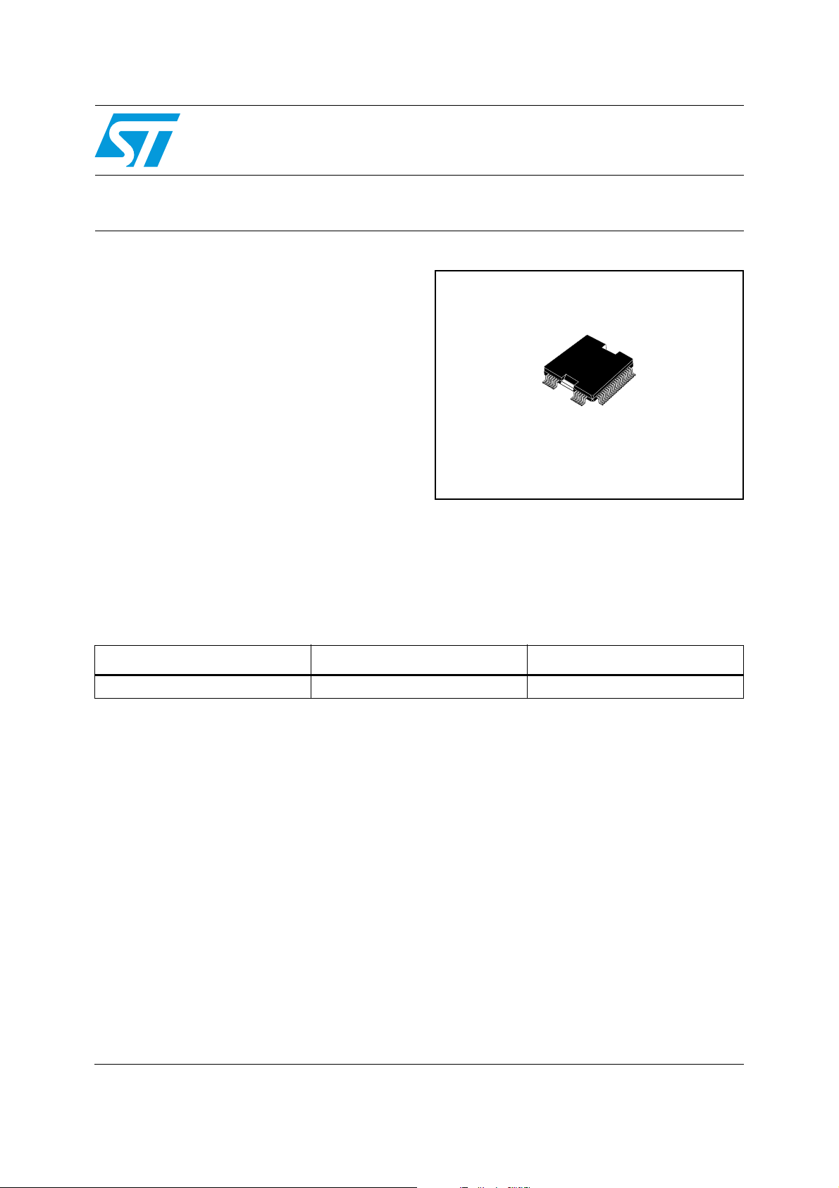
Description
The TDA7570 is a switchmode power audio
amplifier with differential inputs and PWM output.
Table 1. Device summary
TDA7570
HiQUAD64
The maximum output current and voltage swing
are depending by the output circuitry (power
supply, external power transistors and sensing
resistors). The device can work as a stereo
single-ended channels or a mono bridge power
amplifier.
Order code Package Packing
TDA7570 HiQUAD64 Tray
August 2007 Rev 1 1/17
www.st.com
17

Contents TDA7570
Contents
1 Block and simplified application diagram . . . . . . . . . . . . . . . . . . . . . . . 3
2 Pin description . . . . . . . . . . . . . . . . . . . . . . . . . . . . . . . . . . . . . . . . . . . . . 4
3 Electrical specifications . . . . . . . . . . . . . . . . . . . . . . . . . . . . . . . . . . . . . . 7
3.1 Absolute maximum ratings . . . . . . . . . . . . . . . . . . . . . . . . . . . . . . . . . . . . . 7
3.2 Thermal data . . . . . . . . . . . . . . . . . . . . . . . . . . . . . . . . . . . . . . . . . . . . . . . 7
3.3 Electrical characteristics . . . . . . . . . . . . . . . . . . . . . . . . . . . . . . . . . . . . . . . 7
3.4 Notes on the electrical schematic shown in Figure 3 . . . . . . . . . . . . . . . . 11
3.4.1 Main characteristics . . . . . . . . . . . . . . . . . . . . . . . . . . . . . . . . . . . . . . . . 11
4 Functions, pins and components description . . . . . . . . . . . . . . . . . . . 12
4.1 Components with critical placement and type: . . . . . . . . . . . . . . . . . . . . . 12
4.2 Input capacitors . . . . . . . . . . . . . . . . . . . . . . . . . . . . . . . . . . . . . . . . . . . . 12
4.3 Short circuit protection current calculation . . . . . . . . . . . . . . . . . . . . . . . . 12
4.4 External thermal protection network . . . . . . . . . . . . . . . . . . . . . . . . . . . . . 13
4.5 Gate driving network . . . . . . . . . . . . . . . . . . . . . . . . . . . . . . . . . . . . . . . . 13
4.6 External connections . . . . . . . . . . . . . . . . . . . . . . . . . . . . . . . . . . . . . . . . 13
5 Package informations . . . . . . . . . . . . . . . . . . . . . . . . . . . . . . . . . . . . . . . 15
6 Revision history . . . . . . . . . . . . . . . . . . . . . . . . . . . . . . . . . . . . . . . . . . . 16
2/17
TDA7570 Block and simplified application diagram
1 Block and simplified application diagram
Figure 1. Block and simplified application diagram
5V DIG
5V DIG
IN L+
IN L-
I-OFCLK
O0-15
CDsel1
CDsel2
NTC
THWint
THWext
2.5V
-2.5V
MUTE
ST-BY
IN R+
IN R-
PGND
FEED L IN +V
40
46
45
33
34
OSC
29
30
CLIP
31
CD
38
36
TERM.
37
54
52
REF
55
56
49
50
10
5332
SGNDDGND -VS +V
-VS +V
LEFT
CHANNEL
SIGNAL
PROCESSING
RIGHT
CHANNEL
SIGNAL
PROCESSING
REFL
REFL
S -VREF1
INTERFACE
INTERFACE
-VS +V
REFL
+V
S
CHANNEL LEFT
HSD +
PROTECTIONS
CHANNEL LEFT
LSD +
PROTECTIONS
CHANNEL RIGHT
HSD +
PROTECTIONS
CHANNEL RIGHT
LSD +
PROTECTIONS
26,27,58,592557 60 61
-V
S
+VS -L
OW
4212928
SNR1
SPI1
13
14
SPI2
18
GPL
17
GPLS
22
GNLS
21
GNL
23
SNL2
24
SNL1
+V
-5
6
S
+5
15
-V
S
8
SPR1
7
SPR2
4
GPR
5
GPRS
63
GNRS
64
GNR
62
SNR2
+25V
OUTPUT
LOWPASS
FILTER
-25V
+25V
OUTPUT
LOWPASS
FILTER
-25V
OUT LEFT
OUT RIGHT
D00AU1198
3/17
Pin description TDA7570
2 Pin description
Figure 2. Pins connection diagram
N.C.
N.C.
N.C.
Gpr
Gprs
+Vs-5
Spr2
Spr1
+Vs-Vref1
pgnd
N.C.
+Vs
Spl1
Spl2
-Vs+5
N.C.
Gpls
Gpl
N.C.
N.C.
Gnrs
Gnr
63
64
1
2
3
4
5
6
7
8
9
10
12
13
14
15
16
17
18
19
20
21 22 23 24 25
Gnl
Gnls
62
Snr2
Snl2
61
Snr1
60
Snl1
-Vs
-Vs+Vrefr
59
26
-Vs
-Vs+Vrefl
Feed R in
ST-BY
MUTE
CDsel1
CDsel2
+2.5V
CD
-Vs
58
57 56 55 54 53
271128 29 30 31 32
-Vs
Feed L in
sgnd
dgnd
52
51
50
49
48
47
46
45
44
43
42
41
40
39
38
37
36
35
34
33
-2.5V
N.C.
IN R-
IN R+
N.C.
N.C.
IN L+
IN L-
N.C.
N.C.
+Vs-low
N.C.
5Vdig
N.C.
NTC
THWext
THWint
N.C.
O0-I5
I-O-FCLK
AC00241
Table 2. Pins description
Pin
number
Name Function
1 N.C. Not connected
2 N.C. Not connected
3 N.C. Not connected
4 Gpr Gate PMOS, right channel +Vs-12V 30V
5 Gprs Sense gate PMOS, right channel +Vs-12V 30V
6+Vs-5 +Vs-6
7 Spr2 Sensing 2 PMOS, right channel 30V
8 Spr1 Sensing 1 PMOS, right channel 30V
9 +Vs-Vref1 Supply drivers PMOS +Vs-12V 30V
10 pgnd Power ground 0 (ref.)
11 N.C. Not connected
4/17
Voltage l i m i t
(low)
Voltage l i m i t
(high)

TDA7570 Pin description
Table 2. Pins description (continued)
Pin
number
12 +Vs Positive power supply 30V
13 Spl1 Sensing 1 PMOS, left channel 30V
14 Spl2 Sensing 2 PMOS, left channel 30V
15 -Vs+5 -Vs+6
16 N.C. Not connected
17 Gpls Sense gate PMOS, left channel +Vs-12V 30V
18 Gpl Gate PMOS, left channel +Vs-12V 30V
19 N.C. Not connected
20 N.C. Not connected
21 Gnl Gate NMOS, left channel -30V -Vs+12V
22 Gnls Gate NMOS, left channel -30V -Vs+12V
23 Snl2 Sensing 2 NMOS, left channel -30V
24 Snl1 Sensing 1 NMOS, left Channel -30V
25 -Vs+Vrefl Supply drivers NMOS. left channel -30V -Vs+12V
26 -Vs Negative power supply -30V
27 -Vs Negative power supply -30V
28 Feed L in Feedback network left channel -5V 5V
Name Function
Voltage l i m i t
(low)
Voltage l i m i t
(high)
29 CDsel1 Clip detector selection 1 5.5V
30 CD sel2 Clip detector selection 2 5.5V
31 CD Clip detector output 5.5V
32 dgnd Digital ground 0 (ref)
33 I-O-FCLK Clock frequency input/output pin 5.5V
34 O0-I5
35 N.C. Not connected
36 THWint Internal thermal warning output 5.5V
37 THWext External thermal warning output 5.5V
38 NTC Sensing resistors network 5.5V
39 N.C. Not connected
40 5Vdig Digital 5V supply output 5.5V
41
42 +Vs-low Positive voltage supply low power 30V
43 N.C. Not connected
44 N.C. Not connected
Input/output FCLK selection
0 = Output; 1 = Input
5.5V
5/17

Pin description TDA7570
Table 2. Pins description (continued)
Pin
number
45 IN L- Left channel negative input -3V 3V
46 IN L+ Left channel positive input -3V 3V
47 N.C. Not connected
48 N.C. Not connected
49 IN R+ Right channel positive input -3V 3V
50 IN R- Right channel negative input -3V 3V
51 N.C. Not connected
52 -2.5V Signal -2.5V supply output -2.75V
53 sgnd Signal ground 0 (ref)
54 +2.5V Signal 2.5V supply output 2.75V
55 MUTE Mute input 5.5V
56 ST-BY Stand by input 6V
57 Feed R in Feedback network right channel -5 5V
58 -Vs Negative voltage supply -30V
59 -Vs Negative voltage supply -30V
60 -Vs+Vrefr Supply drivers NMOS. Right channel -30V -Vs+12V
61 Snr1 Sensing 2 NMOS, right channel -30V
Name Function
Voltage l i m i t
(low)
Voltage l i m i t
(high)
62 Snr2 Sensing 1 NMOS, right channel -30V
63 Gnrs Sense gate NMOS, right channel -30V -Vs+12V
64 Gnr Gate NMOS, right channel -30V -Vs+12V
6/17

TDA7570 Electrical specifications
3 Electrical specifications
3.1 Absolute maximum ratings
Table 3. Absolute maximum ratings
Symbol Parameter Value Unit
±V
P
T
T
Operating supply voltage ±30 V
s
Power dissipation T
tot
Junction temperature, operating range -40 to 150 °C
j
Storage temperature, operating range -55 to 150 °C
stg
= 85°C 21 W
case
3.2 Thermal data
Table 4. Thermal data
Symbol Parameter Value Unit
R
th j-case
Thermal resistance junction to case 3 °C/W
3.3 Electrical characteristics
Table 5. Electrical characteristics
Symbol Parameter Test condition Min. Typ. Max. Unit
±V
S
I
q
I
st-by
V
os
(V
= ±25V, RL = 4Ω, f = 100Hz, Tj = 25°C, Gain = 28dB, application circuit shown in
S
Figure 3, 2x65/1x130W system, unless otherwise specified.)
Operating supply voltage ±12 ±30 V
V
Quiescent supply current
Quiescent supply current
Output offset voltage
= 5V, F
st-by
V
= 0 from +VS0.35 0.5 0.65 mA
st-by
V
= 0 from -VS-0.2 -0.3 -0.4 mA
st-by
Output-GND (single-ended) 350 mV
Output L - Output R (bridge) 120 mV
switching
= 352.8kHz
from +V
from +VS -low
from -V
20
S
5.4
20
S
25
25
35
7
9
35
mA
mA
mA
P
Output Power
o
Power dissipation of the
P
d
TDA7570
Single-ended, @ THD = 1%
2 x 70W system
Bridge, @ THD = 1%
1 x 250W system
70 W
250 W
Quiescent condition 1.5 1.75 W
7/17

Electrical specifications TDA7570
Table 5. Electrical characteristics (continued)
(V
= ±25V, RL = 4Ω, f = 100Hz, Tj = 25°C, Gain = 28dB, application circuit shown in
S
Figure 3, 2x65/1x130W system, unless otherwise specified.)
Symbol Parameter Test condition Min. Typ. Max. Unit
P
Power dissipation of the external
dt
power transistors (total)
THD Total harmonic distortion
@ P
= 25W, bridge
out
configuration
= 10 W, single ended 0.1 %
@ P
out
@ P
= 40 W, bridge 0.03 0.1 %
out
10 W
G Gain single-ended 27 28 29 dB
G Gain Bridge 33 34 35 dB
Output noise Single_Ended "A" weighted 200 μV
E
n
E Output noise bridge "A" weighted 150 μV
ΔG
R
R
Delta gain error between
e
channels
Input resistance Single-ended 7 10 13 KΩ
i
Input resistance Bridge 3.5 5 6.5 KΩ
i
f = 1kHz, after output filter of TBD
order, 20kHz butterworth
0.5 dB
Threshold voltage of the
V
gspth
Pchannel Vgs sensor
2.533.5V
(VSpx1 - VGpxs)
Threshold voltage of the
V
gsnth
Pchannel Vgs sensor
2.533.5V
(VGnxs - VSnx1)
c
Crosstalk f = 1kHz, Vo = 2Vrms 50 60 dB
t
A
SVR Supply voltage rejection f = 100Hz, V
F
V
Mute attenuation Vo = 2Vrms 70 80 dB
m
= 0.5V 50 60 dB
r
Switching frequency 250 310 360 KHz
SW
Logic inputs low level voltage 1.5 V
V
il
Logic inputs high level voltage 2.3 V
ih
CLIP DETECTOR
Vcd
Clip detector pin max operating
voltage (open drain)
5.5 V
CDl Clip detector pin leakage current CD off 1 μA
CDs
CDi Clip detector THD intervention
Clip detector pin saturation
voltage
CD on, 1mA 1 V
CDsel1=0, CDsel2=0
(near clipping detection)
0.5 %
CDsel1=0, CDsel2=1 1 %
CDsel1=1, CDsel2=0 5 %
CDsel1=1, CDsel2=1 8 %
8/17

TDA7570 Electrical specifications
Table 5. Electrical characteristics (continued)
(V
= ±25V, RL = 4Ω, f = 100Hz, Tj = 25°C, Gain = 28dB, application circuit shown in
S
Figure 3, 2x65/1x130W system, unless otherwise specified.)
Symbol Parameter Test condition Min. Typ. Max. Unit
PROTECTIONS
T
hwc
T
sdc
T
sdch
T
hws
T
sds
T
sdsh
V
pp
V
pn
I
spx1
I
snx1
DRIVERS
V
hgp
V
lgp
V
hgn
V
lgn
I
hgp
I
lgp
Chip thermal warning intervention
150 °C
Thermal shut-down chip 160 °C
Thermal shut-down chip hysteresis
External thermal warning
intervention
External thermal shut-down
intervention
External thermal shut-down
hysteresis
Protection intervention voltage
Pchannel (Vspx1-Vspx2)
Protection intervention voltage
Nchannel (Vsnx2-Vsnx1)
5Vdig
x 0.45
5Vdig
x 0.37
5Vdig
x 0.03
85 100 120 mV
85 100 120 mV
10 °C
7
5Vdig
x 0.48
5Vdig
x 0.4
5Vdig
x 0.04
5Vdig
x 0.51
5Vdig
x 0.43
5Vdig
x 0.043
V
V
V
Current input pins 7, 13 150 200 260 μA
Current output pins 24, 61 -150 -200 -260 μA
High level output voltage (Gpl, Gpr)
Low level output voltage (Gpl, Gpr)
High level output voltage (Gnl, Gnr)
Low level output voltage (Gnl, Gnr)
High level output sink current
(Gpl, Gpr, peak)
Low level output source current
(Gpl, Gpr, peak)
+Vs-10 V
+V
s
-V
s
-Vs+10 V
2.2 A
2.7 A
V
V
I
I
High level output sink current
hgn
(Gnl, Gnr, peak)
Low level output source current
lgn
(Gnl, Gnr, peak)
2.5 A
1.7 A
INTERNAL POWER SUPPLY
5Vdig 5Vdig pin output voltage Reference: dgnd pin 4.3 4.8 5.3 V
2.5V 2.5V pin output voltage Reference: sgnd pin 2.15 2.4 2.65 V
-2.5V -2.5V pin output voltage Reference: sgnd pin -2.15 -2.4 -2.65 V
Vref1 Vref1 pin output voltage Reference: + Vs pin 8.6 9.6 10.6 V
Vrefl/Vrefr
Vrefl, Vrefr pin output voltage Reference: - Vs pin -8.6 -9.6 -10.6 V
9/17

Electrical specifications TDA7570
Figure 3. Application diagrams
10/17

TDA7570 Electrical specifications
3.4 Notes on the electrical schematic shown in Figure 3
3.4.1 Main characteristics
● 2 channels single-ended or 1 channel bridge PWM amplifier
● Power output: see Tab l e 5
● Gain single-ended = 28 dB
● Gain bridge = 34dB
● Clip detector settled at THD=10%
● Internal master oscillator
The schematic is depicted showing the suggested structure of the printed circuit board
tracks (star points, high current path, components placement).
To avoid malfunctioning due to the parasitic inductance, short connections lengths are
recommended.
Table 6. Component characteristics
Component
(See schematic of Figure 4)
P-MOS-L
P-MOS-R
N-MOS-L
N-MOS-R
Rp-N-L2
RP-P-L2
Rp-N-R2
Rp-P-R2
Minimum load:
2 x 4 Ohm single-ended
or 8 Ohm bridge
(2 x 65W / 1 x 130W)
STP12PF06
STP14NF06
Not present 4.7K
Minimum load:
2 x 2 Ohm single-ended
or 4Ohm bridge
(2 x 125W / 1 x 250W))
2 x STP12PF06
in parallel
2 x STP14NF06
in parallel
11/17

Functions, pins and components description TDA7570
4 Functions, pins and components description
4.1 Components with critical placement and type:
● Ci-L1, Ci-L2, Ci-R1, Ci-R2 must be placed as near as possible to the sources of the
respective power MOS. If 2 power MOS in parallel are needed, can be useful to place a
couple of capacitors for each couple of power MOS. These capacitors are needed to
absorb the high di/dt current present during the Pchannel/Nchannel and
Nchannel/Pchannel transition that can cause high peak voltages on the power supply
wiring connection due to their parasitic inductance.
● The capacitors placed between +Vs to GND and to -Vs are distributed along the power
lines. With P.C. board with very short connections, some of these capacitors can be
avoided (Cvs-1, Cvs-2, Cd3, Cd4, Cd5, Cd6).
● The current sensing resistors Rsens-N-L, Rsens-P-L, Rsens-P-R and Rsens-N-R must
be not inductive components, as example, made by a costant an wire.
4.2 Input capacitors
● The value of the input capacitors (Cin-L+, Cin-L-, Cin-R+, Cin-R- depends on the
desired -3dB high pass cutoff frequency, following the formula:
F3dB()
--------------------------------------------- -=
6.28 10000 C
1
⋅⋅
in
4.3 Short circuit protection current calculation
Figure 4. Short circuit protection current diagram (example for the N-channel)
TDA7570
(not inductive resistor)
Rsens
Typ. Values = 10 – 30 mOhm
to -Vs
Imos
Rp1 (typ=4.7kOhm)
Cfil (typ 2.2nF)
Rfil (typ. 100 Ohm)
Vfil = Ispx1 x Rfil = 20mV Typ
I
lim
lim
----------------- -
Rsens
I
----------------- -
=
Rsens
1
SPx2 pin
Rp2
1
Vpx Rp1 Rp2+()⋅
⎛⎞
------------------------------------------------- - Vfil+
⎝⎠
Vpx Vfil+()=
Rp2
← if Rp2 is not used
Vp=100mV Typ
comparator
SPx1 pin
12/17

TDA7570 Functions, pins and components description
4.4 External thermal protection network
Example of external thermal protection circuitry
● Components:
– type: B57621 C621/100k/+
–R
● Results (simulations):
text
= 10K
– External thermal warning temperature intervention: 90 °C
– External thermal shut down temperature intervention: 100 °C
– External thermal shut down hysteresis: 6 °C
4.5 Gate driving network
The main purpose of the 27 Ohm resistors Rd-N-L, Rd-P-L, Rd-N-R and Rd-P-R are the
following:
● 1) Dumping of the L-C equivalent circuit done by the parasitic inductance and
capacitance present in the circuit
● 2) Reduction of the dv/dt of the Vgs and then reduction of the di/dt of the drain current
of the power MOS.
The R-C snubber network done by:
– Rs-N-L, Cs-N-L
–Rs-P-L, Cs-P-L
– Rs-N-R, Cs-N-R
– Rs-P-R, Cs-P-R
Are in the direction to increase the dumping (point 1) and reduce the dv/dt (point 2.
The value of these components is also depending on the layout structure. With a reduction
of the parasitic inductance present in the P.C. board layout, in the region around the power
transistors, the value of these components can be reduced, giving advantage in terms of
THD, mainly at mid-high power levels, due to the reduction of the "dead zone".
The minimum suggested value of Rd-x-x is around 10Ω, while, is some cases, Rs-x-x and
Cs-x-x can be removed.
4.6 External connections
● CD, THWEXT, THWINT
These pins, if used, it must be connected to a pull-up resistor (>10kΩ) connected to a
supply voltage referred to the receiver device (as example, a μP). Max 10V.
● MUTE - To have a soft mute-play and play-mute transition, an R-C network can be
applied (as example 47kΩ, 1μF)
● ST-BY - To avoid pop noise due to multiple ST-BY parasitic pulses, an R-C network can
be added (as example 47kΩ, 0.1μF)
● +V
-low - This pin supply the low voltage circuits. It can be connected to the +Vs or to
s
a reference voltage comprising between 12V to +Vs.
13/17

Functions, pins and components description TDA7570
A connection to +Vs through a 100Ω resistor, together a 1μF capacitor placed from
+Vs-low and GND is possible too.
● NL+, INL-, INR+, INR- Input pins. The sign is referred to the input of the differential-to-
singleended amplifier. Because the power stage is an inverting stage, the output of the
amplifier is with opposite sign with respect these pins. For bridge operation, the
connection INL+ must be shorted to the INR- and the connection INL- must be shorted
to INR+
14/17

TDA7570 Package informations
5 Package informations
In order to meet environmental requirements, ST offers these devices in ECOPACK®
packages. These packages have a Lead-free second level interconnect. The category of
second level interconnect is marked on the package and on the inner box label, in
compliance with JEDEC Standard JESD97. The maximum ratings related to soldering
conditions are also marked on the inner box label. ECOPACK is an ST trademark.
ECOPACK specifications are available at: www.st.com.
Figure 5. HiQUAD-64 mechanical data and package dimensions
DIM.
mm inch
MIN. TYP. MAX. MIN. TYP. MAX.
A 3.15 0.124
A1 0 0.25 0 0.010
A2 2.50 2.90 0.10 0.114
A3 0 0.10 0 0.004
b 0.22 0.38 0.008 0.015
c 0.23 0.32 0.009 0.012
D 17.00 17.40 0.669 0.685
D1 (1) 13.90 14.00 14.10 0.547 0.551 0.555
D2 2.65 2.80 2.95 0.104 0.110 0.116
E 17.00 17.40 0.669 0.685
E1 (1) 13.90 14.00 14.10 0.547 0.551 0.555
e 0.65 0.025
E2 2.35 2.65 0.092 0.104
E3 9.30 9.50 9.70 0.366 0.374 0.382
E4 13.30 13.50 13.70 0.523 0.531 0.539
F 0.10 0.004
G 0.12 0.005
L 0.80 1.10 0.031 0.043
N10
S
(1): "D1" and "E1" do not inclu de mold flash or protusions
- Mold flash or protusions shall not exceed 0.15mm(0.006inch) per side
A
53
°
(max.)
0°
(min.), 7˚(max.)
N
A
b
⊕
33
M
F AB
OUTLINE AND
MECHANICAL DATA
HiQUAD-64
E2
c
BOTTOM VIEW
e
A2
E3
D2
(slug tail width)
64
E
POQU64ME
B
Gauge Plane
0.35
E1
slug
(bottom side)
1
E4 (slug lenght)
D1
D
21
E3
SEATING PLANE
COPLANARITY
C
G
C
A3
S
L
A1
15/17

Revision history TDA7570
6 Revision history
Table 7. Document revision history
Date Revision Changes
29-Aug-2007 1 Initial release.
16/17

TDA7570
Please Read Carefully:
Information in this document is provided solely in connection with ST products. STMicroelectronics NV and its subsidiaries (“ST”) reserve the
right to make changes, corrections, modifications or improvements, to this document, and the products and services described herein at any
time, without notice.
All ST products are sold pursuant to ST’s terms and conditions of sale.
Purchasers are solely responsible for the choice, selection and use of the ST products and services described herein, and ST assumes no
liability whatsoever relating to the choice, selection or use of the ST products and services described herein.
No license, express or implied, by estoppel or otherwise, to any intellectual property rights is granted under this document. If any part of this
document refers to any third party products or services it shall not be deemed a license grant by ST for the use of such third party products
or services, or any intellectual property contained therein or considered as a warranty covering the use in any manner whatsoever of such
third party products or services or any intellectual property contained therein.
UNLESS OTHERWISE SET FORTH IN ST’S TERMS AND CONDITIONS OF SALE ST DISCLAIMS ANY EXPRESS OR IMPLIED
WARRANTY WITH RESPECT TO THE USE AND/OR SALE OF ST PRODUCTS INCLUDING WITHOUT LIMITATION IMPLIED
WARRANTIES OF MERCHANTABILITY, FITNESS FOR A PARTICULAR PURPOSE (AND THEIR EQUIVALENTS UNDER THE LAWS
OF ANY JURISDICTION), OR INFRINGEMENT OF ANY PATENT, COPYRIGHT OR OTHER INTELLECTUAL PROPERTY RIGHT.
UNLESS EXPRESSLY APPROVED IN WRITING BY AN AUTHORIZED ST REPRESENTATIVE, ST PRODUCTS ARE NOT
RECOMMENDED, AUTHORIZED OR WARRANTED FOR USE IN MILITARY, AIR CRAFT, SPACE, LIFE SAVING, OR LIFE SUSTAINING
APPLICATIONS, NOR IN PRODUCTS OR SYSTEMS WHERE FAILURE OR MALFUNCTION MAY RESULT IN PERSONAL INJURY,
DEATH, OR SEVERE PROPERTY OR ENVIRONMENTAL DAMAGE. ST PRODUCTS WHICH ARE NOT SPECIFIED AS "AUTOMOTIVE
GRADE" MAY ONLY BE USED IN AUTOMOTIVE APPLICATIONS AT USER’S OWN RISK.
Resale of ST products with provisions different from the statements and/or technical features set forth in this document shall immediately void
any warranty granted by ST for the ST product or service described herein and shall not create or extend in any manner whatsoever, any
liability of ST.
ST and the ST logo are trademarks or registered trademarks of ST in various countries.
Information in this document supersedes and replaces all information previously supplied.
The ST logo is a registered trademark of STMicroelectronics. All other names are the property of their respective owners.
© 2007 STMicroelectronics - All rights reserved
STMicroelectronics group of companies
Australia - Belgium - Brazil - Canada - China - Czech Republic - Finland - France - Germany - Hong Kong - India - Israel - Italy - Japan -
Malaysia - Malta - Morocco - Singapore - Spain - Sweden - Switzerland - United Kingdom - United States of America
www.st.com
17/17
 Loading...