

Quad power amplifier with integrated step-up converter
Features
■ Multipower BCD technology
■ DMOS power output
■ Non-switching high efficiency amplifier
■ Switching high efficiency voltage converter
■ High output power capability:
– 4 x 41 W max @ V
– 4 x 59 W @ V
■ Full I
2
C bus driving:
– Standby
– Independent front/rear soft play/mute
– Selectable gain 26 dB - 12 dB (for low noise
line output function)
– High efficiency enable/disable
– Voltage converter enable/disable
– Regulated voltage selection
– Switching frequency selection
■ Hardware mute function
■ Full fault protection
■ DC offset detection
■ Four independent short circuit protection
■ Clipping detector with selectable threshold
(1 % / 10 %) via I
Table 1. Device summary
= 14.4 V
s
= 14.4 V and PWM = 17.5 V
s
2
C bus
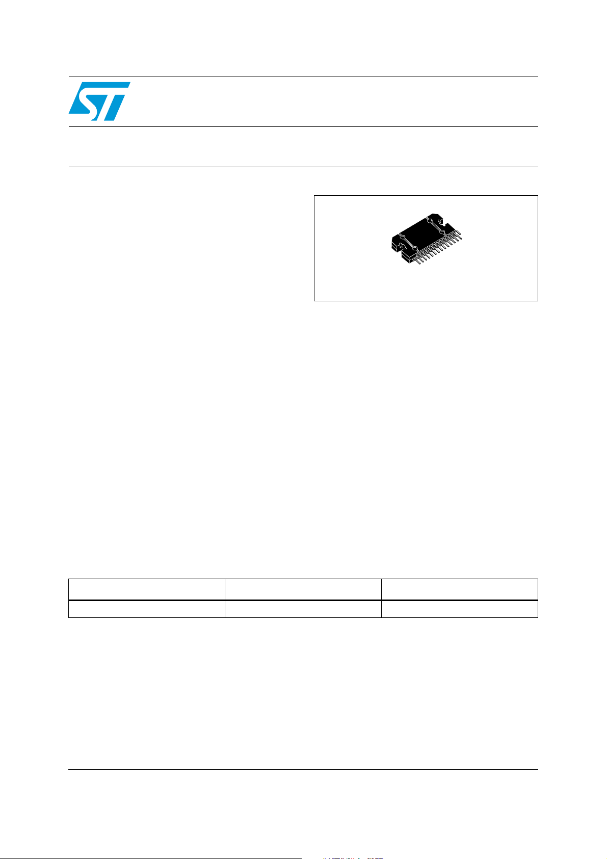
TDA7565
Flexiwatt27
Description
The TDA7565 is a new BCD technology quad
bridge type of car radio amplifier in Flexiwatt27
package specially intended for car radio
applications.
Thanks to the DMOS output stage the TDA7565
has a very low distortion allowing a clear powerful
sound.
The built-in voltage converter control block
assures a very high output power with an
extremely low number of added components.
Furthermore, the converter makes the TDA7565
compliant to the most recent OEM specifications
for low voltage operation (so called 'start-stop'
battery profile during engine stop), helping car
manufacturers to reduce the overall emissions
and thus contributing to environment protection.
Order code Package Packing
TDA7565 Flexiwatt27 Tube
February 2010 Doc ID 9800 Rev 4 1/19
www.st.com
1

Contents TDA7565
Contents
1 Block and pin connection diagrams . . . . . . . . . . . . . . . . . . . . . . . . . . . . 5
2 Electrical specification . . . . . . . . . . . . . . . . . . . . . . . . . . . . . . . . . . . . . . . 6
2.1 Absolute maximum ratings . . . . . . . . . . . . . . . . . . . . . . . . . . . . . . . . . . . . . 6
2.2 Thermal data . . . . . . . . . . . . . . . . . . . . . . . . . . . . . . . . . . . . . . . . . . . . . . . 6
2.3 Electrical characteristics . . . . . . . . . . . . . . . . . . . . . . . . . . . . . . . . . . . . . . . 6
3I
2
C bus interface . . . . . . . . . . . . . . . . . . . . . . . . . . . . . . . . . . . . . . . . . . . 10
3.1 Data validity . . . . . . . . . . . . . . . . . . . . . . . . . . . . . . . . . . . . . . . . . . . . . . . 10
3.2 Start and stop conditions . . . . . . . . . . . . . . . . . . . . . . . . . . . . . . . . . . . . . 10
3.3 Byte format . . . . . . . . . . . . . . . . . . . . . . . . . . . . . . . . . . . . . . . . . . . . . . . . 10
3.4 Acknowledge . . . . . . . . . . . . . . . . . . . . . . . . . . . . . . . . . . . . . . . . . . . . . . 10
4 Software specifications . . . . . . . . . . . . . . . . . . . . . . . . . . . . . . . . . . . . . 12
5 Examples of bytes sequence . . . . . . . . . . . . . . . . . . . . . . . . . . . . . . . . . 15
6 Low voltage "start-stop" operation . . . . . . . . . . . . . . . . . . . . . . . . . . . . 16
7 Package information . . . . . . . . . . . . . . . . . . . . . . . . . . . . . . . . . . . . . . . . 17
8 Revision history . . . . . . . . . . . . . . . . . . . . . . . . . . . . . . . . . . . . . . . . . . . 18
2/19 Doc ID 9800 Rev 4

TDA7565 List of tables
List of tables
Table 1. Device summary . . . . . . . . . . . . . . . . . . . . . . . . . . . . . . . . . . . . . . . . . . . . . . . . . . . . . . . . . . 1
Table 2. Absolute maximum ratings . . . . . . . . . . . . . . . . . . . . . . . . . . . . . . . . . . . . . . . . . . . . . . . . . . 6
Table 3. Thermal data. . . . . . . . . . . . . . . . . . . . . . . . . . . . . . . . . . . . . . . . . . . . . . . . . . . . . . . . . . . . . 6
Table 4. Electrical characteristics . . . . . . . . . . . . . . . . . . . . . . . . . . . . . . . . . . . . . . . . . . . . . . . . . . . . 6
Table 5. Chip address. . . . . . . . . . . . . . . . . . . . . . . . . . . . . . . . . . . . . . . . . . . . . . . . . . . . . . . . . . . . 12
Table 6. IB1 . . . . . . . . . . . . . . . . . . . . . . . . . . . . . . . . . . . . . . . . . . . . . . . . . . . . . . . . . . . . . . . . . . . 12
Table 7. IB2 . . . . . . . . . . . . . . . . . . . . . . . . . . . . . . . . . . . . . . . . . . . . . . . . . . . . . . . . . . . . . . . . . . . 13
Table 8. DB1. . . . . . . . . . . . . . . . . . . . . . . . . . . . . . . . . . . . . . . . . . . . . . . . . . . . . . . . . . . . . . . . . . . 13
Table 9. DB2. . . . . . . . . . . . . . . . . . . . . . . . . . . . . . . . . . . . . . . . . . . . . . . . . . . . . . . . . . . . . . . . . . . 13
Table 10. DB3. . . . . . . . . . . . . . . . . . . . . . . . . . . . . . . . . . . . . . . . . . . . . . . . . . . . . . . . . . . . . . . . . . . 14
Table 11. DB4. . . . . . . . . . . . . . . . . . . . . . . . . . . . . . . . . . . . . . . . . . . . . . . . . . . . . . . . . . . . . . . . . . . 14
Table 12. Document revision history . . . . . . . . . . . . . . . . . . . . . . . . . . . . . . . . . . . . . . . . . . . . . . . . . 18
Doc ID 9800 Rev 4 3/19

List of figures TDA7565
List of figures
Figure 1. Block diagram . . . . . . . . . . . . . . . . . . . . . . . . . . . . . . . . . . . . . . . . . . . . . . . . . . . . . . . . . . . . 5
Figure 2. Pin connection (top view) . . . . . . . . . . . . . . . . . . . . . . . . . . . . . . . . . . . . . . . . . . . . . . . . . . . 5
Figure 3. Demoboard schematic . . . . . . . . . . . . . . . . . . . . . . . . . . . . . . . . . . . . . . . . . . . . . . . . . . . . . 9
Figure 4. Data validity on the I2C bus . . . . . . . . . . . . . . . . . . . . . . . . . . . . . . . . . . . . . . . . . . . . . . . . 10
Figure 5. Timing diagram on the I2C bus. . . . . . . . . . . . . . . . . . . . . . . . . . . . . . . . . . . . . . . . . . . . . . 11
Figure 6. Acknowledge on the I2C bus . . . . . . . . . . . . . . . . . . . . . . . . . . . . . . . . . . . . . . . . . . . . . . . 11
Figure 7. Worst case condition for a start-stop system diagram . . . . . . . . . . . . . . . . . . . . . . . . . . . . 16
Figure 8. Flexiwatt27 (vertical) mechanical data and package dimensions . . . . . . . . . . . . . . . . . . . . 17
4/19 Doc ID 9800 Rev 4
TDA7565 Block and pin connection diagrams
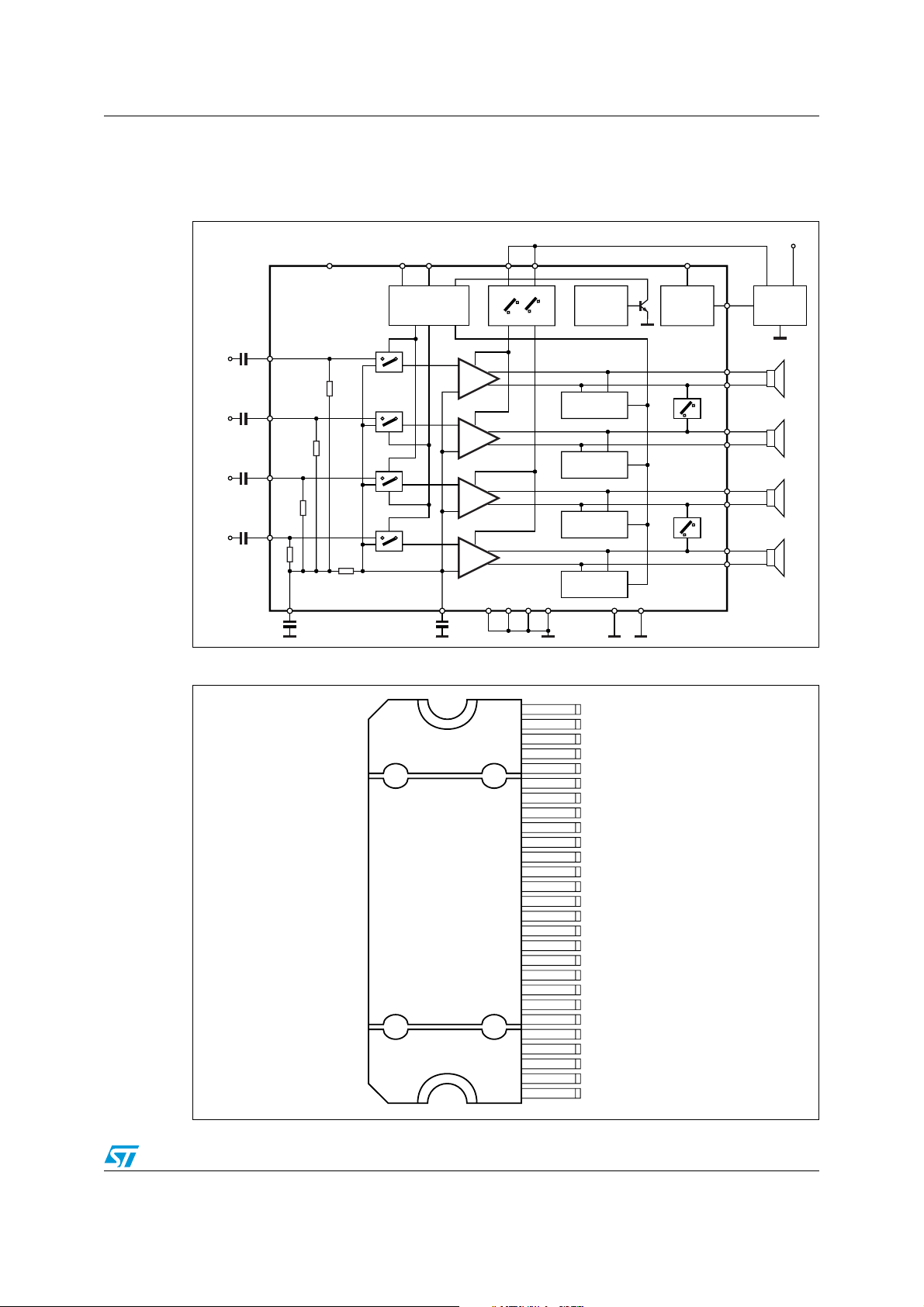
A
1 Block and pin connection diagrams
Figure 1. Block diagram
V
S
MUTE
CLK
V
CC1
V
CC2DATA CC GND
I2C BUS
MUTE1
MUTE2
IN RF
IN RR
IN LF
IN LR
F
R
F
R
SVR RF RR LF LR TAB S_GNDAC_GND
Figure 2. Pin connection (top view)
12/26dB
12/26dB
12/26dB
12/26dB
PW_GND
27
26
25
24
23
22
21
20
19
18
17
16
15
14
13
12
11
10
9
8
7
6
5
4
3
2
1
CLIP
DETECTOR
SHORT CIRCUIT
PROTECTION
SHORT CIRCUIT
PROTECTION
SHORT CIRCUIT
PROTECTION
SHORT CIRCUIT
PROTECTION
MUTE
DATA
PW_GND RR
OUT RR-
CK
OUT RR+
V
CC2
OUT RF-
PW_GND RF
OUT RF+
AC_GND
IN RF
IN RR
S_GND
IN LR
IN LF
SVR
OUT LF+
PW_GND LF
OUT LF-
V
CC1
OUT LR+
CC GND
OUT LR-
PW_GND LR
MG
TAB
D00AU1233
VOLTAGE
CONVERTER
CONTROL
MG
OUT RF+
OUT RF-
OUT RR+
OUT RR-
OUT LF+
OUT LF-
OUT LR+
OUT LR-
D00AU1232A
VOLTAGE
CONVERTER
EXTERNAL
CIRCUIT
Doc ID 9800 Rev 4 5/19
Electrical specification TDA7565
2 Electrical specification
2.1 Absolute maximum ratings
Table 2. Absolute maximum ratings
Symbol Parameter Value Unit
V
opc OFF
V
opc ON
V
V
peak
V
V
DATA
I
I
P
T
stg
Operating supply voltage, converter off 18 V
Operating supply voltage, converter on 25 V
DC supply voltage 28 V
S
Peak supply voltage (for t = 50 ms) 50 V
CK pin voltage 6 V
CK
Data pin voltage 6 V
Output peak current (not repetitive t = 100 µs) 8 A
O
Output peak current (repetitive f > 10 Hz) 6 A
O
Power dissipation T
tot
, TjStorage and junction temperature -55 to 150 °C
2.2 Thermal data
Table 3. Thermal data
Symbol Description Value Unit
R
th j-case
Thermal resistance junction to case Max. 1 °C/W
= 70 °C 80 W
case
2.3 Electrical characteristics
Refer to the test circuit, VS = 14.4 V; RL = 4 Ω; f = 1 kHz; voltage converter disabled (VC
T
= 25 °C; unless otherwise specified.
amb
Table 4. Electrical characteristics
Symbol Parameter Test condition Min. Typ. Max. Unit
Power amplifier
V
S
I
d
I
d
P
O
6/19 Doc ID 9800 Rev 4
Supply voltage range - 8 - 18 V
Total quiescent drain current - - 250 300 mA
Total quiescent drain current
(VCon)
Output power
(VC
)
off
V = 14.4 V
--350-mA
Max power
THD = 10 %
THD = 1 %
(1)
-41-W
22
18
27
22
-
W
W
Off
);

TDA7565 Electrical specification
Table 4. Electrical characteristics (continued)
Symbol Parameter Test condition Min. Typ. Max. Unit
Output power
(VCon)
P
O
V = 14.4V, PWM = 17.5V
Max power
THD = 10 %
THD = 1 %
(1)
-59-W
32
25
39
31
-
W
W
0.03
-
0.03
0.1
0.1
-6070μV
-1525μV
THD Total harmonic distortion
C
Cross talk f = 1 kHz to 10 kHz, RG = 600 Ω 50 55 - dB
T
R
G
ΔG
G
ΔG
E
E
Input impedance - 60 100 130 KΩ
IN
Voltage gain 1 - 25.5 26 26.5 dB
V1
Voltage gain match 1 - -1 - 1 dB
V1
Voltage gain 2 - 11.5 12 12.5 dB
V2
Voltage gain match 2 - -1 - 1 dB
V2
Output noise voltage 1
IN1
Output noise voltage 2
IN2
SVR Supply voltage rejection
P
= 1 W to 12 W; STDmode
O
HE mode; PO = 1-2 W
HE mode; P
= 1-12 W, f = 10 kHz - 0.15 0.5 %
P
O
= 4-12 W
O
Rg = 600 Ω; GV = 26 dB
filter 20 Hz to 22 kHz
Rg = 600 Ω; GV = 26 dB
filter 20 Hz to 12 kHz
f = 100 Hz to 10 kHz; V
= 600 Ω
R
g
= 1V pk;
r
50 60 - dB
BW Power bandwidth (-3 dB) 75 - - KHz
A
V
V
Standby attenuation - 70 100 dB
SB
I
Standby current - - - 50 μA
SB
Mute attenuation - 70 90 dB
A
M
Offset voltage Mute and play -100 - 100 mV
OS
Min. supply voltage threshold - 6.5 7 7.5 V
AM
Slew rate - 1.5 - - V/μs
T
T
Turn on delay D2/D1 (IB1) 0 to 1 - 10 40 ms
ON
Turn off delay D2/D1 (IB1) 1 to 0 - 10 40 ms
OFF
Thermal foldback junction
temperature
- 155 170 185 °C
%
%
%
CD
T
Clip det thd. level
THD
V
Offset detection
O
Thermal warning - - 165 - °C
hw
D0 (IB1) = 1 5 10 15 %
Power amplifier = play
AC Input = 0
±1.5 ±2 ±2.5 V
Doc ID 9800 Rev 4 7/19
D0 (IB1) = 0 0 1 2 %

Electrical specification TDA7565
Table 4. Electrical characteristics (continued)
Symbol Parameter Test condition Min. Typ. Max. Unit
I2C bus interface
f
V
V
Min(pin27)
V
Mout(pin27)
A
M(pin 27)
Clock frequency - - - 400 KHz
SCL
V
Input low voltage - - - 1.5 V
IL
Input high voltage - 2.3 - - V
IH
Mute in threshold voltage Amp. mute - - 1.5 V
Mute out threshold voltage - 3.5 - - V
Mute attenuation - 80 90 - -
Voltage converter
V
V
V
V
V
mgclamp
V
(VC
1. Saturated square wave output.
Converter output voltage
,
cc1
(VC = ON)
cc2
Voltage converter switching
F
s
frequency
MOS gate output low voltage Io = 200 mA - 1 2 V
mgl
MOS gate output high voltage
mgh
MOS gate output clamp voltage Io = 5 mA - 11.5 - V
Fall time Co = 1 nF - 20 - ns
t
f
t
Rise time Co = 1 nF - 50 - ns
r
MOS gate output voltage with
mgl
)
voltage converter disabled
off
= 14 V
V
S
D3 (IB2) = 0; D6 (IB2) = 0
D3 (IB2) = 1; D6 (IB2) = 0
D3 (IB2) = 0; D6 (IB2) = 1
D3 (IB2) = 1; D6 (IB2) = 1
D6 (IB1) = 0; D7 (IB1) = 0
D6 (IB1) = 1; D7 (IB1) = 0
D6 (IB1) = 0; D7 (IB1) = 1
D6 (IB1) = 1; D7 (IB1) = 1
I
= 20 mA - 11 - V
o
I
= 200 mA - 9.5 - V
o
I
= 5 mA - - 0.5 V
o
90
135
230
360
15
16.5
17.5
18.5
-
-V
120
175
300
470
kHz
8/19 Doc ID 9800 Rev 4

TDA7565 Electrical specification
Figure 3. Demoboard schematic
C10 2.2nF
R5 10 1W
V
V
(Vbatt)
S
2200μF
L1 100μH
C7
C9
10nF
R4
3.3
1W
C8
220nF
IN RF
IN RR
R1 50Ω
Q1
R3 10Ω
STP60NE06
C1 220nF
C2 220nF
2
16
15
STPS30L40CT
D1
C11
3300μF
SDASCLDGND
C12
100nF
TDA7565
C3 220nF
IN LF
C4 220nF
IN LR
MUTE
12
13
11 17
27
C6
10μF
14 1
C5
1μF
CC
C13
10μF
21
72623
5
251939
18
20
22
24
10
8
6
4
OUT RF+
OUT RF-
OUT RR+
OUT RR-
OUT LF+
OUT LF-
OUT LR+
OUT LR-
D00AU1224B
Doc ID 9800 Rev 4 9/19

I2C bus interface TDA7565
3 I2C bus interface
Data transmission from microprocessor to the TDA7565 and vice versa takes place through
the 2 wires I
2
C bus interface, consisting of the two lines SDA and SCL (pull-up resistors to
positive supply voltage must be connected).
3.1 Data validity
As shown by Figure 4, the data on the SDA line must be stable during the high period of the
clock. The HIGH and LOW state of the data line can only change when the clock signal on
the SCL line is LOW.
3.2 Start and stop conditions
As shown by Figure 5 a start condition is a high to low transition of the SDA line while SCL is
HIGH. The stop condition is a low to high transition of the SDA line while SCL is high.
3.3 Byte format
Every byte transferred to the SDA line must contain 8 bits. Each byte must be followed by an
acknowledge bit. The MSB is transferred first.
3.4 Acknowledge
The transmitter* puts a resistive high level on the SDA line during the acknowledge clock
pulse (see Figure 6). The receiver** the acknowledges has to pull-down (low) the SDA line
during the acknowledge clock pulse, so that the SDA line is stable low during this clock
pulse.
* Transmitter
–master (μP) when it writes an address to the TDA7565
– slave (TDA7565) when the μP reads a data byte from TDA7565
** Receiver
– slave (TDA7565) when the μP writes an address to the TDA7565
– master (µP) when it reads a data byte from TDA7565
Figure 4. Data validity on the I
SDA
SCL
STABLE, DATA
2
DATA LINE
VALID
C bus
CHANGE
DATA
ALLOWED
D99AU1031
10/19 Doc ID 9800 Rev 4

TDA7565 I2C bus interface
Figure 5. Timing diagram on the I2C bus
SCL
2
CBUS
I
SDA
START
Figure 6. Acknowledge on the I
SCL
SDA
START
1
MSB
D99AU1032
2
C bus
23789
D99AU1033
STOP
ACKNOWLEDGMENT
FROM RECEIVER
Doc ID 9800 Rev 4 11/19

Software specifications TDA7565
4 Software specifications
All the functions of the TDA7565 are activated by I2C interface.
The bit 0 of the "ADDRESS BYTE" defines if the next bytes are write instruction (from µP to
TDA7565) or read instruction (from TDA7565 to µP).
Table 5. Chip address
Bit Instruction
D7 Address bit
D6 Address bit
D5 Address bit
D4 Address bit
D3 Address bit
D2 Address bit
D1 Address bit
Read/Write bit
D0(R/W)
0 = Write instruction
1 = read instruction
If R/W = 0, the µP sends 2 "Instruction Bytes": IB1 and IB2.
Table 6. IB1
Bit Instruction
D7 Sel. freq. switch 1
D6 Sel. freq. switch 2
D5
D4
D3
D2
D1
D0
Offset detection start (D5 = 1)
Offset detection stop (D5 = 0) (off)
Front channel
Gain = 26dB (D4 = 0)
Gain = 12dB (D4 = 1)
Rear channel
Gain = 26dB (D3 = 0)
Gain = 12dB (D3 = 1)
Mute front channels (D2 = 0)
Unmute front channels (D2 = 1)
Mute rear channels (D1 = 0)
Unmute rear channels (D1 = 1)
CD 1% (D0 = 0)
CD 10% (D0 = 1)
12/19 Doc ID 9800 Rev 4

TDA7565 Software specifications
Table 7. IB2
Bit Instruction
D7
Voltage converter enabled (D7 = 1)
Voltage converter disabled (D7 = 0)
D6 Regulated voltage selection 1
D5 Test speed
D4
Stand-by on - amplifier not working - (D4 = 0)
Stand-by off - amplifier working - (D4 = 1)
D3 Regulated voltage selection 0)
D2 To be forced to “Level 1”
Right channel
D1
Power amplifier working in standard mode (D1 = 0)
Power amplifier working in Hi Eff. mode(D1 = 1)
Left channel
D0
Power amplifier working in standard mode (D0 = 0)
Power amplifier working in Hi Eff. mode(D0 = 1)
Table 8. DB1
Bit Instruction
D7 Thermal warning
D6 X
D5 X
D4 X
D3 X
D2 Offset (LF)
D1 Short circuit protection (CH1)
D0 X
Table 9. DB2
Bit Instruction
D7 Off status
D6 X
D5 Clip detector output
D4 X
D3 X
D2 Offset (LR)
D1 Short circuit protection (CH2)
D0 X
Doc ID 9800 Rev 4 13/19

Software specifications TDA7565
Table 10. DB3
Bit Instruction
D7 Standby status
D6 X
D5 X
D4 X
D3 X
D2 Offset (RF)
D1 Short circuit protection (CH3)
D0 X
Table 11. DB4
Bit Instruction
D7 X
D6 X
D5 X
D4 X
D3 X
D2 Offset (RR)
D1 Short circuit protection (CH4)
D0 X
14/19 Doc ID 9800 Rev 4

TDA7565 Examples of bytes sequence
5 Examples of bytes sequence
1 - Turn-on of the power amplifier with 26 dB gain, mute on, diagnostic defeat, high eff.
mode, voltage converter disabled.
Start Address byte with D0 = 0 ACK IB1 ACK IB2 ACK STOP
XX00X000 0XX1XX10
2 - Turn-off of the power amplifier
Start Address byte with D0 = 0 ACK IB1 ACK IB2 ACK STOP
XXXXXXXX XXX0XXX0
4 - Offset detection procedure start
Start Address byte with D0 = 0 ACK IB1 ACK IB2 ACK STOP
XX1XX11X XXX1XXX0
5 - Offset detection procedure stop and reading operation.
Start Address byte with D0 = 1 ACK DB1 STOP
● The purpose of this test is to check if a D.C. offset (2V typ.) is present on the outputs,
produced by input capacitor with anomalous leakage current or humidity between pins.
● The delay from 3 to 4 can be selected by software, starting from 1 ms
Doc ID 9800 Rev 4 15/19

Low voltage "start-stop" operation TDA7565
6 Low voltage "start-stop" operation
The most recent OEM specification are requiring automatic stop of car engine at traffic lights
in order to reduce emissions of polluting substances. The TDA7565, thanks to its integrated
switching voltage converter, allows a continuous operation when battery falls down to 6/7 V
during such conditions, without producing pop noise. The maximum system power will be
reduced accordingly.
The internal converter must be enabled and programmed in order to supply 15 V (D3 (IB2) = 0;
D6 (IB2) = 0). The suggested voltage frequency switching is 150 kHz (D6 (IB1) = 1; D7 (IB1) = 0).
The following curve is a worst case condition for a start-stop system. The TDA7565, with the
switching converter powered on, can sustain this cranking curve without any audio signal
interruption.
Figure 7. Worst case condition for a start-stop system diagram
V
V
b1
Vb3
V
b2
tr
V
= 12 V, Vb2 = 6 V, Vb3 = 7 V
b1
R
≤ 0.01 Ω (internal resistor of power supply)
i
t2 t
1
t
3
t
f
t
Recovery time from test start to tr is 1 s
t
= 2 ms
r
t
= 1 ms (the shortest time, at cranking simulation power supply, is 5 ms)
1
t
= 15 ms
2
t
= 1 s
3
t
= 0.5 s
f
16/19 Doc ID 9800 Rev 4

TDA7565 Package information
7 Package information
In order to meet environmental requirements, ST offers these devices in different grades of
ECOPACK
®
packages, depending on their level of environmental compliance. ECOPACK
®
specifications, grade definitions and product status are available at: www.st.com.
ECOPACK
®
is an ST trademark.
Figure 8. Flexiwatt27 (vertical) mechanical data and package dimensions
DIM.
A 4.45 4.50 4.65 0.175 0.177 0.183
B 1.80 1.90 2.00 0.070 0.074 0.079
C 1.40 0.055
D 0.75 0.90 1.05 0.029 0.035 0.041
E 0.37 0.39 0.42 0.014 0.015 0.016
F (1) 0.57 0.022
G 0.80 1.00 1.20 0.031 0.040 0.047
G1 25.75 26.00 26.25 1.014 1.023 1.033
H (2) 28.90 29.23 29.30 1.139 1.150 1.153
H1 17. 00 0.669
H2 12. 80 0.503
H3 0.80 0.031
L (2) 22.07 22.47 22.87 0.869 0.884 0.904
L1 18.57 18.97 19.37 0.731 0.747 0.7 62
L2 (2) 15.50 15.70 15.90 0.610 0.618 0.626
L3 7.70 7.85 7.95 0.303 0.309 0.313
L4 5 0.197
L5 3.5 0.138
M 3.70 4.00 4.30 0.145 0.157 0.169
M1 3.60 4.00 4.40 0.142 0.157 0.173
N 2.20 0.086
O 2 0.079
R 1.70 0.067
R1 0.5 0.02
R2 0.3 0.12
R3 1.25 0.049
R4 0.50 0.019
V5˚ (Typ.)
V1 3˚ (Typ.)
V2 20˚ (Typ.)
V3 45˚ (Typ.)
(1): dam-ba r protusion no t included
(2): molding pr otusion incl uded
mm inch
MIN. TYP. MAX. MIN. TYP. MA X.
OUTLINE AND
MECHANICAL DATA
Flexiwatt27 (vertical)
V
C
B
H
V3
OL3 L4
L2
Pin 1
H3
G
H1
G1
H2
R3
N
F
V
A
R4
R2
R
L
L1
V2
R2
FLEX27ME
V1
R1
L5
R1 R1
M1
M
V1
D
E
7139011
Doc ID 9800 Rev 4 17/19

Revision history TDA7565
8 Revision history
Table 12. Document revision history
Date Revision Changes
20-Sep-2003 1 Initial release.
1-Jul-2008 2
25-Jan-2010 3
03-Feb-2010 4 Minor text changes.
Document reformatted.
Document status promoted from product preview to datasheet.
Updated Features and Description on page 1.
Updated Table 4: Electrical characteristics.
Added Section 6: Low voltage "start-stop" operation.
18/19 Doc ID 9800 Rev 4

TDA7565
Please Read Carefully:
Information in this document is provided solely in connection with ST products. STMicroelectronics NV and its subsidiaries (“ST”) reserve the
right to make changes, corrections, modifications or improvements, to this document, and the products and services described herein at any
time, without notice.
All ST products are sold pursuant to ST’s terms and conditions of sale.
Purchasers are solely responsible for the choice, selection and use of the ST products and services described herein, and ST assumes no
liability whatsoever relating to the choice, selection or use of the ST products and services described herein.
No license, express or implied, by estoppel or otherwise, to any intellectual property rights is granted under this document. If any part of this
document refers to any third party products or services it shall not be deemed a license grant by ST for the use of such third party products
or services, or any intellectual property contained therein or considered as a warranty covering the use in any manner whatsoever of such
third party products or services or any intellectual property contained therein.
UNLESS OTHERWISE SET FORTH IN ST’S TERMS AND CONDITIONS OF SALE ST DISCLAIMS ANY EXPRESS OR IMPLIED
WARRANTY WITH RESPECT TO THE USE AND/OR SALE OF ST PRODUCTS INCLUDING WITHOUT LIMITATION IMPLIED
WARRANTIES OF MERCHANTABILITY, FITNESS FOR A PARTICULAR PURPOSE (AND THEIR EQUIVALENTS UNDER THE LAWS
OF ANY JURISDICTION), OR INFRINGEMENT OF ANY PATENT, COPYRIGHT OR OTHER INTELLECTUAL PROPERTY RIGHT.
UNLESS EXPRESSLY APPROVED IN WRITING BY AN AUTHORIZED ST REPRESENTATIVE, ST PRODUCTS ARE NOT
RECOMMENDED, AUTHORIZED OR WARRANTED FOR USE IN MILITARY, AIR CRAFT, SPACE, LIFE SAVING, OR LIFE SUSTAINING
APPLICATIONS, NOR IN PRODUCTS OR SYSTEMS WHERE FAILURE OR MALFUNCTION MAY RESULT IN PERSONAL INJURY,
DEATH, OR SEVERE PROPERTY OR ENVIRONMENTAL DAMAGE. ST PRODUCTS WHICH ARE NOT SPECIFIED AS "AUTOMOTIVE
GRADE" MAY ONLY BE USED IN AUTOMOTIVE APPLICATIONS AT USER’S OWN RISK.
Resale of ST products with provisions different from the statements and/or technical features set forth in this document shall immediately void
any warranty granted by ST for the ST product or service described herein and shall not create or extend in any manner whatsoever, any
liability of ST.
ST and the ST logo are trademarks or registered trademarks of ST in various countries.
Information in this document supersedes and replaces all information previously supplied.
The ST logo is a registered trademark of STMicroelectronics. All other names are the property of their respective owners.
© 2010 STMicroelectronics - All rights reserved
STMicroelectronics group of companies
Australia - Belgium - Brazil - Canada - China - Czech Republic - Finland - France - Germany - Hong Kong - India - Israel - Italy - Japan -
Malaysia - Malta - Morocco - Philippines - Singapore - Spain - Sweden - Switzerland - United Kingdom - United States of America
www.st.com
Doc ID 9800 Rev 4 19/19
 Loading...