

CD00108485 Rev 1.0 ACTIVE PAGE A
AM/FM Car Radio Tuner IC with Stereo Decoder and Intelligent
Selectivity System (ISS)
Datasheet
DOCUMENT HISTORY
Version Release Date Change Qualifier
Rev 1.0 Initial Release
Initial Edocs version
CD00108485 Rev 1.0 ACTIVE PAGE B
DOCUMENT APPROVAL
Name Function Date
Brasca, Guido Market Com 11−May−2006
Bosisio, Savino Corporate Com 11−May−2006
CD00108485 Rev 1.0 ACTIVE PAGE C
REFERENCED DOCUMENTS
Document Id Document Type Document Title Relation Name
No References

CD00108485 Rev 1.0 ACTIVE PAGE D
CUSTOM ATTRIBUTES
Alternate Identifier(s) 12326
Alternate Name
Confidentiality Level Public
ECN Number
Original ID
Original Repository
Revalidation Date
Status ACTIVE
Publishing scope Public
Root Part Number(s) TDA7540B
DOCUMENT CD00108485 REVISION 1.0 ACTIVE DATE 11-May-2006 page: 1/75
TDA7540B
AM/FM Car Radio Tuner IC with Stereo Decoder and
Intelligent Selectivity System (ISS)
Features
FM-Part
■ RF AGC generation by RF and IF detection
■ I/Q mixer for 1st FM IF 10.7MHz with image
rejection
■ Mixer for 2nd IF 450kHz
■ Internal 450KHz bandpass filter with bandwidth
control by ISS
■ Fully integrated FM-demodulator with spike
cancellation
AM-Part
■ Wide and narrow AGC generation
■ Mixer for 1st IF 10.7MHz, AM upconversion
■ Mixer for 2nd IF 450kHz, AM downconversion
■ Integrated AM-demodulator
■ AM IF- and audio noise blanking
Stereodecoder
■ PLL with adjustment free, fully integrated VCO
■ Automatic pilot dependent MONO/STEREO
switching
■ Programmable ROLL-OFF compensation
■ High cut and stereo blend-characteristics
programmable
■ Dedicated RDS-mute
■ Internal noise blanker with several threshold
controls
Additional Features
■ VCO for world tuning range
■ High performance fast PLL for RDS-System
■ IF counter for FM and AM with search stop
signal
■ Quality detector for level, deviation, adjacent
channel and multipath
■ ISS (Intelligent Selectivity System) for
cancellation of adjacent channel and noise
influences
■ Adjacent channel mute
■ Fully electronic alignment
■ All functions I
Description
The TDA7540 is a high performance tuner circuit
for AM/FM car radio. It contains mixer, IF
amplifier, demodulator for AM and FM,
stereodecoder, quality detection, ISS filter and
PLL synthesizer with IF counter on a single chip.
Use of BICMOS technology allows the
implementation of several tuning functions and a
minimum of external components.
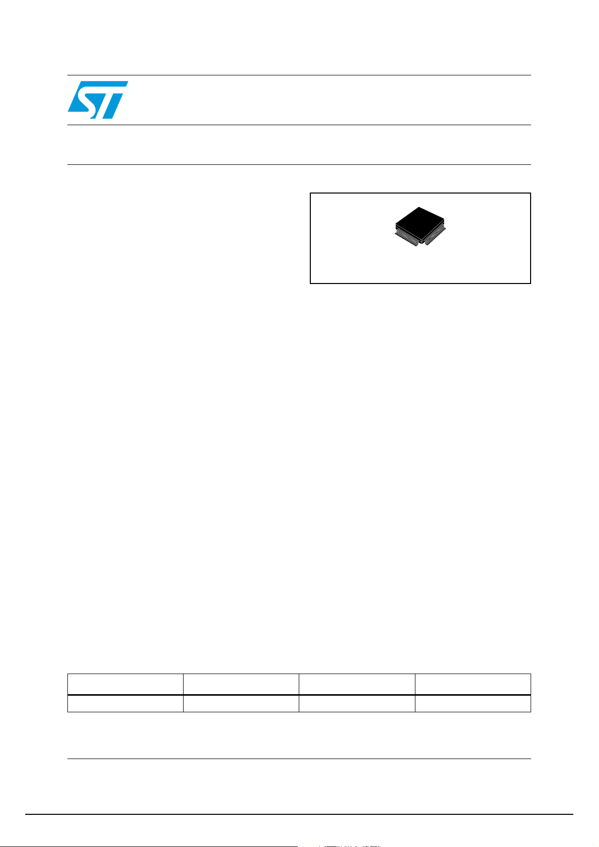
TQFP80
2
C-Bus controlled
Order codes
Part number Temp range, °CPackage Packing
TDA7540B -40 to 85 TQFP80 Tube
May 2006 Rev 1 1/75
www.st.com
Copyright STMicroelectronics COMPANY INTERNAL Unauthorized reproduction and communication strictly prohibited
75

DOCUMENT CD00108485 REVISION 1.0 ACTIVE DATE 11-May-2006 page: 2/75
Contents TDA7540B
Contents
1 Block diagram . . . . . . . . . . . . . . . . . . . . . . . . . . . . . . . . . . . . . . . . . . . . . . 4
2 Pins description and connection diagrams . . . . . . . . . . . . . . . . . . . . . . 5
2.1 TQFP80 pins connection diagram . . . . . . . . . . . . . . . . . . . . . . . . . . . . . . . 5
2.2 Pin description . . . . . . . . . . . . . . . . . . . . . . . . . . . . . . . . . . . . . . . . . . . . . . 5
2.3 Thermal data . . . . . . . . . . . . . . . . . . . . . . . . . . . . . . . . . . . . . . . . . . . . . . . 7
3 Electrical specifications . . . . . . . . . . . . . . . . . . . . . . . . . . . . . . . . . . . . . . 8
3.1 Absolute maximum ratings . . . . . . . . . . . . . . . . . . . . . . . . . . . . . . . . . . . . . 8
3.2 Electrical characteristics . . . . . . . . . . . . . . . . . . . . . . . . . . . . . . . . . . . . . . . 8
3.2.1 Globals . . . . . . . . . . . . . . . . . . . . . . . . . . . . . . . . . . . . . . . . . . . . . . . . . . . 8
3.2.2 FM section . . . . . . . . . . . . . . . . . . . . . . . . . . . . . . . . . . . . . . . . . . . . . . . . 9
3.2.3 AM section . . . . . . . . . . . . . . . . . . . . . . . . . . . . . . . . . . . . . . . . . . . . . . . 14
3.2.4 Stereodecoder . . . . . . . . . . . . . . . . . . . . . . . . . . . . . . . . . . . . . . . . . . . . 16
3.2.5 PLL section . . . . . . . . . . . . . . . . . . . . . . . . . . . . . . . . . . . . . . . . . . . . . . 22
4 Functional description . . . . . . . . . . . . . . . . . . . . . . . . . . . . . . . . . . . . . . 24
4.1 FM section . . . . . . . . . . . . . . . . . . . . . . . . . . . . . . . . . . . . . . . . . . . . . . . . 24
4.1.1 Mixer1, AGC and 1.IF . . . . . . . . . . . . . . . . . . . . . . . . . . . . . . . . . . . . . . 24
4.1.2 Mixer2, limiter and demodulator . . . . . . . . . . . . . . . . . . . . . . . . . . . . . . . 24
4.1.3 Quality detection and ISS . . . . . . . . . . . . . . . . . . . . . . . . . . . . . . . . . . . 24
4.1.4 Soft mute control . . . . . . . . . . . . . . . . . . . . . . . . . . . . . . . . . . . . . . . . . . 25
4.2 AM section . . . . . . . . . . . . . . . . . . . . . . . . . . . . . . . . . . . . . . . . . . . . . . . . 26
4.3 Stereodecoder . . . . . . . . . . . . . . . . . . . . . . . . . . . . . . . . . . . . . . . . . . . . . 26
4.3.1 Decoder . . . . . . . . . . . . . . . . . . . . . . . . . . . . . . . . . . . . . . . . . . . . . . . . . 26
4.3.2 Functional description of the noise blanker . . . . . . . . . . . . . . . . . . . . . . 29
4.3.3 Functional description of the multipath-detector . . . . . . . . . . . . . . . . . . 30
4.3.4 Quality detector . . . . . . . . . . . . . . . . . . . . . . . . . . . . . . . . . . . . . . . . . . . 31
4.3.5 AFS control and stereo decoder mute . . . . . . . . . . . . . . . . . . . . . . . . . . 31
4.4 PLL and if counter section . . . . . . . . . . . . . . . . . . . . . . . . . . . . . . . . . . . . 32
4.4.1 PLL frequency synthesizer block . . . . . . . . . . . . . . . . . . . . . . . . . . . . . . 32
4.4.2 IF counter block . . . . . . . . . . . . . . . . . . . . . . . . . . . . . . . . . . . . . . . . . . . 33
4.5 I2C-Bus interface . . . . . . . . . . . . . . . . . . . . . . . . . . . . . . . . . . . . . . . . . . . 34
2/75
Copyright STMicroelectronics COMPANY INTERNAL Unauthorized reproduction and communication strictly prohibited

DOCUMENT CD00108485 REVISION 1.0 ACTIVE DATE 11-May-2006 page: 3/75
TDA7540B Contents
4.5.1 Data transition . . . . . . . . . . . . . . . . . . . . . . . . . . . . . . . . . . . . . . . . . . . . 34
4.5.2 Start condition . . . . . . . . . . . . . . . . . . . . . . . . . . . . . . . . . . . . . . . . . . . . 34
4.5.3 Stop condition . . . . . . . . . . . . . . . . . . . . . . . . . . . . . . . . . . . . . . . . . . . . 35
4.5.4 Acknowledge . . . . . . . . . . . . . . . . . . . . . . . . . . . . . . . . . . . . . . . . . . . . . 35
4.5.5 Data transfer . . . . . . . . . . . . . . . . . . . . . . . . . . . . . . . . . . . . . . . . . . . . . 35
4.5.6 Device addressing . . . . . . . . . . . . . . . . . . . . . . . . . . . . . . . . . . . . . . . . . 35
4.5.7 Write operation . . . . . . . . . . . . . . . . . . . . . . . . . . . . . . . . . . . . . . . . . . . 35
4.5.8 Read operation . . . . . . . . . . . . . . . . . . . . . . . . . . . . . . . . . . . . . . . . . . . 36
5 Software specification . . . . . . . . . . . . . . . . . . . . . . . . . . . . . . . . . . . . . . 37
5.1 Address organization . . . . . . . . . . . . . . . . . . . . . . . . . . . . . . . . . . . . . . . . 37
5.2 Control register function . . . . . . . . . . . . . . . . . . . . . . . . . . . . . . . . . . . . . . 39
5.2.1 Data Byte Specification . . . . . . . . . . . . . . . . . . . . . . . . . . . . . . . . . . . . . 43
6 Appendix . . . . . . . . . . . . . . . . . . . . . . . . . . . . . . . . . . . . . . . . . . . . . . . . . 63
7 Part List (Application and measurment circuit) . . . . . . . . . . . . . . . . . . 70
8 Application circuit . . . . . . . . . . . . . . . . . . . . . . . . . . . . . . . . . . . . . . . . . . 71
9 Application Notes . . . . . . . . . . . . . . . . . . . . . . . . . . . . . . . . . . . . . . . . . . 72
10 Package Information . . . . . . . . . . . . . . . . . . . . . . . . . . . . . . . . . . . . . . . . 73
11 Revision history . . . . . . . . . . . . . . . . . . . . . . . . . . . . . . . . . . . . . . . . . . . 74
3/75
Copyright STMicroelectronics COMPANY INTERNAL Unauthorized reproduction and communication strictly prohibited
DOCUMENT CD00108485 REVISION 1.0 ACTIVE DATE 11-May-2006 page: 4/75
Block diagram TDA7540B
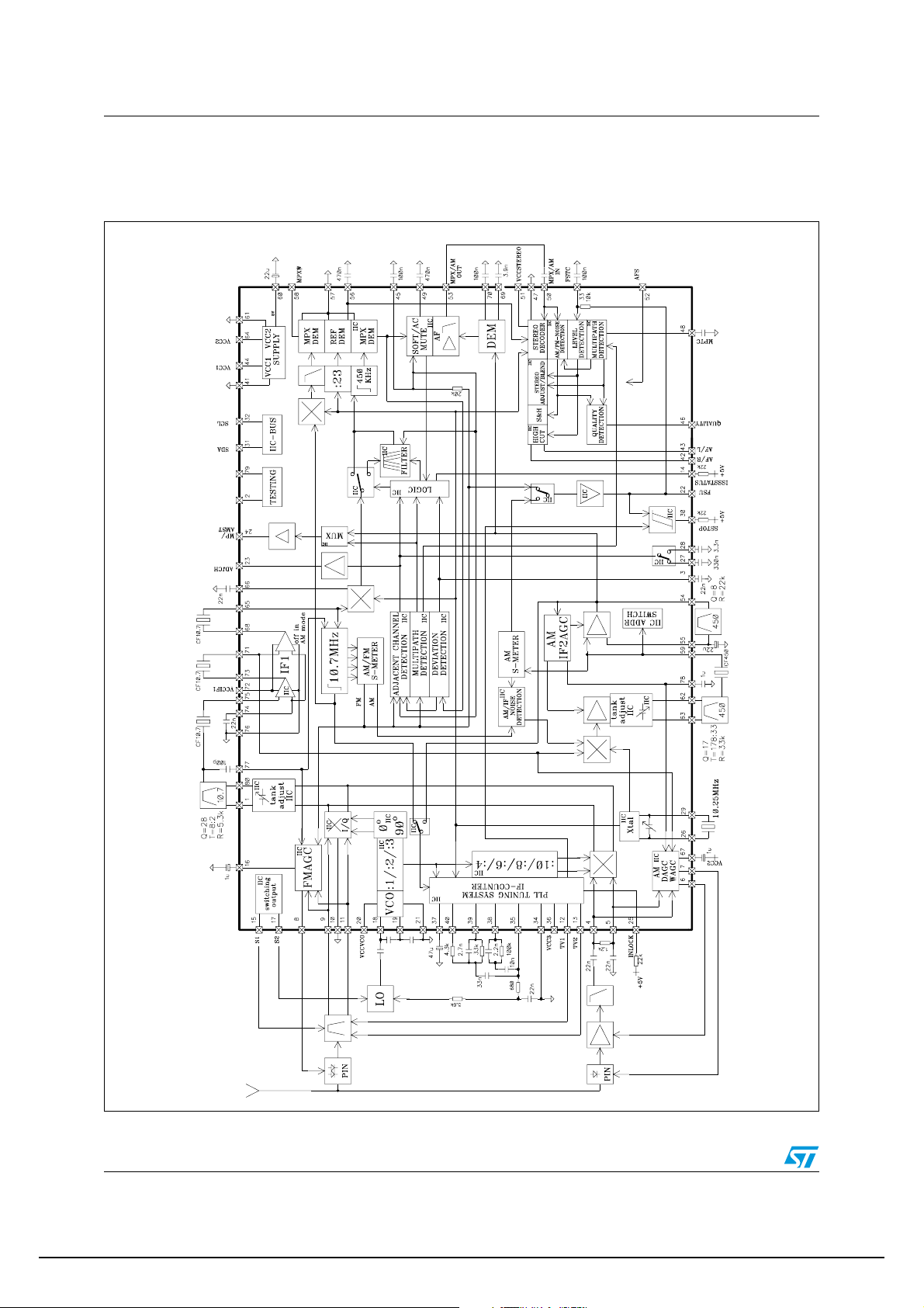
1 Block diagram
Figure 1. Block circuit diagram
4/75
Copyright STMicroelectronics COMPANY INTERNAL Unauthorized reproduction and communication strictly prohibited
DOCUMENT CD00108485 REVISION 1.0 ACTIVE DATE 11-May-2006 page: 5/75
TDA7540B Pins description and connection diagrams
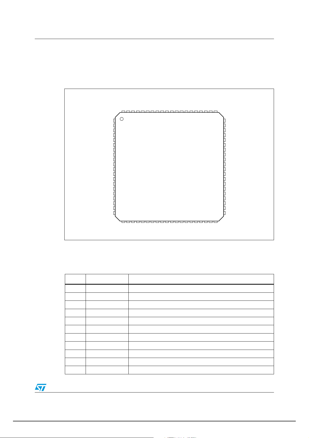
2 Pins description and connection diagrams
2.1 TQFP80 pins connection diagram
Figure 2. TQFP80 pins connection (top view)
IF1AMP1IN
IF1REF
IF1AMP1OUT
VCCIF1
IF1AMP2IN
AMDETC
IF1AMP2OUT
AMRFAGCTC
FMM1X2REF
FMM1X2IN
VCC2
AMMIX2OUT1
AMMIX2OUT2
GNDVCC2
60
59
58
57
56
55
54
53
52
51
50
49
48
47
46
45
44
43
42
41
VREF1
RXIN0AMIF2IN
MPXW
GNDDEM
FMREFDEMC
AMIF2REF
AMIF2BPF
MPXOUT
AFS
VCCSTEREO
MPXIN
MUTETC
MPTC
GNDSTEREO
QUALYOUT
FSWO
VCC1
L
R
GNDVCC1
MIX1 OUT1
TEST1
DEVTC
AMMIX1IN
AMMIX1REF
AMRFAGCOUT
AMPINDR
FMPINDR
FMMIX1IN1
GNDRF
FMMIX1IN2
TV1
TV2
ISSSTATUS
FMAGCTC
VCOB
VCOE
VCCVCO
S1
S2
TEST2
MIX1OUT2
79
80
1
2
3
4
5
6
7
8
9
10
12
13
14
15
16
17
18
19
20
21 22 23 24 25
GNDIF1
IF1AGCIN
AMAGC2TC
75 74 73 727071 69 68 67 66 65
76
77
78
26 27 28 29 30
AMREFDEMC
311132 33 34 35 36
64 63 62 61
37 38 39 40
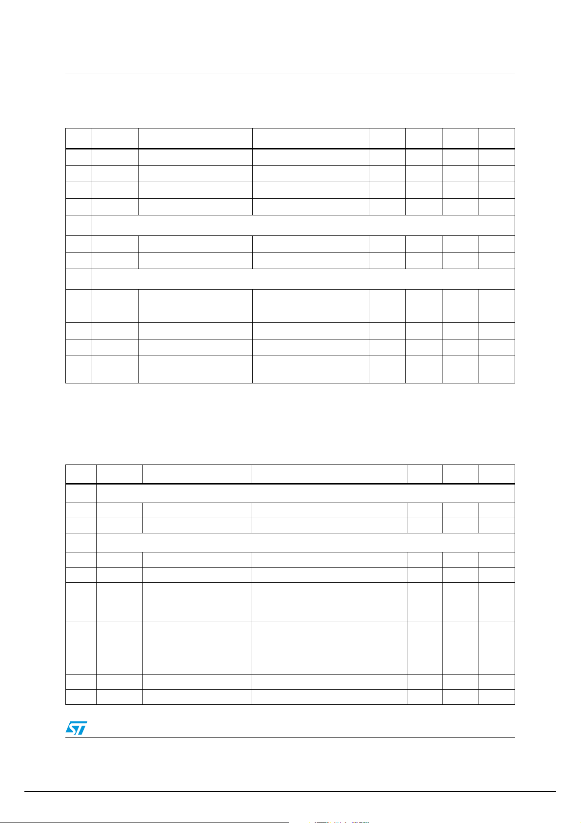
2.2 Pin description
Table 1. Pin description
Pin No. Pin Name Function
1 MIX1OUT1 Mixer Tank 10.7MHz
2 TEST1 Testing I/O Pin
3 DEVTC Deviation Detector Time Constant
4 AMMIX1IN AM Mixer1 Input
5 AMMIX1REF AM Mixer1 Reference
6 AMRFAGCOUT Output AM RF AGC
7 AMPINDR AM PIN Diode Driver Output
8 FMPINDR FM PIN Diode Driver Output
9 FMMIX1IN1 FM Mixer1 Input1
10 GNDRF RF Ground
11 FMMIX1IN2 FM Mixer1 Input2
FSU
GNDVCO
ADJCH
AMST/MP
XTALG
INLOCK
ISSTC1
ISSTC2
XTALD
SSTOP
SDA
SCL
FSTC
LPOUT
GNDVCC3
VCC3
VREF2
LPAM
LPFM
LPHC
D05AU1618
5/75
Copyright STMicroelectronics COMPANY INTERNAL Unauthorized reproduction and communication strictly prohibited

DOCUMENT CD00108485 REVISION 1.0 ACTIVE DATE 11-May-2006 page: 6/75
Pins description and connection diagrams TDA7540B
Table 1. Pin description (continued)
Pin No. Pin Name Function
12 TV1 Tuning Voltage Preselection1
13 TV2 Tuning Voltage Preselection2
14 ISSSTATUS ISS Filter Status Output
15 S1 Free Programmable Switching Output
16 FMAGCTC FM AGC Time Constant
17 S2 Free Programmable Switching Output
18 VCOB VCO Input Base
19 VCOE VCO Output Emitter
20 VCCVCO VCO Supply
21 GNDVCO VCO Ground
22 FSU Unweighted Fieldstrength Output
23 ADJCH Ident. Adjacent Channel Output
24 AMST/MP AM Stereo Output / Ident. Multipath Output
25 INLOCK PLL Inlock Information Output
26 XTALG Xtal Oscillator to MOS Gate
27 ISSTC1 Time Constant1 ISS Filter Switch
28 ISSTC2 Time Constant2 ISS Filter Switch
29 XTALD Xtal Oscillator to MOS Drain
30 SSTOP Search Stop Output
2
31 SDA I
32 SCL I
33 FSTC S-meter Filtering Capacitor
34 GNDVCC3 VCC3 Ground
35 LPOUT Op Amp Output to PLL Loop Filters
36 VCC3 Supply Tuning Voltage
37 VREF2 Voltage Reference for PLL Op Amp
38 LPAM Op Amp Input to PLL Loop Filters AM
39 LPFM Op Amp Input to PLL Loop Filters FM
40 LPHC High Current PLL Loop Filter Input
41 GNDVCC1 Digital Ground
42 R Stereodecoder Output Right
43 L Stereodecoder Output Left
44 VCC1 Digital Supply
45 FSWO Weighted Fieldstrength Output with programmable DC offset
46 Qualyout Stereodecoder Quality Output
47 GNDSTEREO Strereodecoder Ground
48 MPTC Multipath Time Constant
49 MUTETC Weak Signal Mute Time Constant
C-Bus Data
2
C-Bus Clock
6/75
Copyright STMicroelectronics COMPANY INTERNAL Unauthorized reproduction and communication strictly prohibited
DOCUMENT CD00108485 REVISION 1.0 ACTIVE DATE 11-May-2006 page: 7/75
TDA7540B Pins description and connection diagrams
Table 1. Pin description (continued)
Pin No. Pin Name Function
50 MPXIN Stereodecoder Input
51 VCCSTEREO Stereodecoder Supply
52 AFS Alternative Frequency Search Drive
53 MPX/AFAM MPX Output / AM AF Output
54 AMIF2BPF AM IF2 Bandpass Filter
55 AMIF2REF Reference Voltage AM IF2 Amplifier
56 FMREFDEMC FM Demodulator Reference
57 GNDDEM Ground FM Demodulator
58 MPXW MPX Output without ISS Filtering
59 AMIF2IN Input AM IF2
60 VREF1 Reference 5V
61 GNDVCC2 Analog Ground
62 AMMIX2OUT2 AM Tank 450kHz
63 AMMIX2OUT1 AM Tank 450kHz
64 VCC2 Analog Supply
65 FMMIX2IN FM IF1 Mixer2 Input
66 FMMIX2REF FM IF1 Mixer2 Reference
67 AMRFAGCTC AM RF AGC Time Constant
68 IF1AMP2OUT IF1 Amplifier2 Output
69 AMDETC AM Detector Capacitor
70 AMREFDEMC AM Demodulator Reference
71 IF1AMP2IN IF1 Amplifier2 Input
72 VCCIF1 IF1 Supply
73 IF1AMP1OUT IF1 Amplifier1 Output
74 IF1REF IF1 Amplifier Reference
75 IF1AMP1IN IF1 Amplifier1 Input
76 GNDIF1 IF1 Ground
77 IF1AGCIN IF1 AGC Input
78 AMAGC2TC AM AGC2 Time Constant
79 TEST2 Testing I/O Pin
80 MIX1OUT2 Mixer Tank 10.7MHz
2.3 Thermal data
Table 2. Thermal data
Symbol Parameter Value Unit
R
th(j-amb)
Thermal Resistance Junction to ambient Max.
7/75
Copyright STMicroelectronics COMPANY INTERNAL Unauthorized reproduction and communication strictly prohibited
55
°C/W
DOCUMENT CD00108485 REVISION 1.0 ACTIVE DATE 11-May-2006 page: 8/75
Electrical specifications TDA7540B
3 Electrical specifications
3.1 Absolute maximum ratings
Table 3. Absolute maximum rating
Symbol Parameter Value Unit
V
T
T
V
V
V
Supply voltage 9.5 V
S
Ambient temperature -40 to 85 °C
amb
Storage temperature -55 to 150 °C
stg
ESD protection (Human Body Model) ±1500 V
ESD
ESD protection (Machine Model) ±150 V
ESD
ESD protection (Change Device Model) ±750 V
ESD
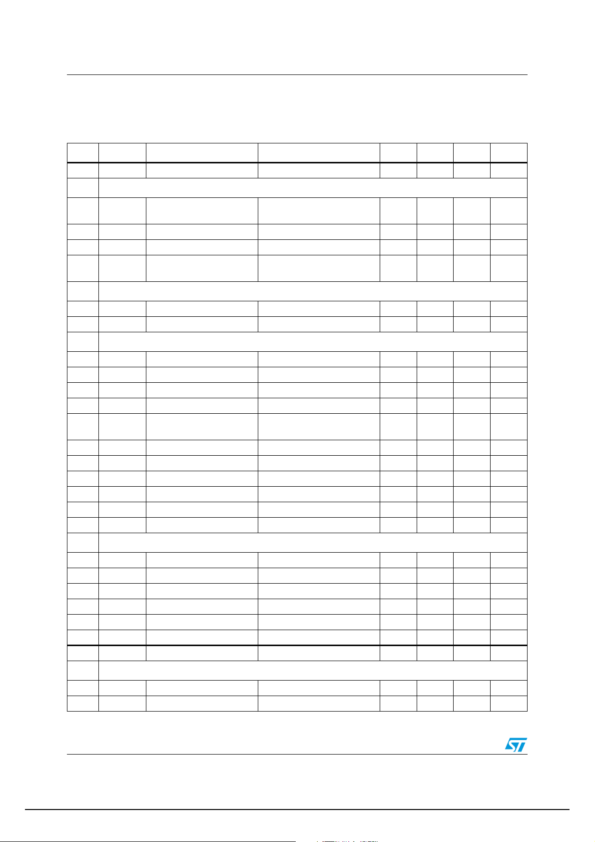
3.2 Electrical characteristics
3.2.1 Globals
Table 4. Electrical characteristics
Item Symbol Parameter Test conditions Min. Typ. Max. Unit
1 Supply
1.1 V
1.2 V
1.3 V
1.4 V
1.5 V
1.6 V
1.7 V
1.8 V
1.9 I
1.10 I
1.11 I
1.12 I
1.13 I
1.14 I
1.15 I
(T
f
Xtal
CC1
CC2
CC3
CCVCO
CCMIX1
CCMIX2
CCIF1
CCST
CC1
CC1
CC2
CC2
CC3
CCVCO
CCMIX1
= 25°C, V
amb
CC1
= V
CC2
= V
CC3
= V
CCST
= V
CCVCO
= V
CCMIX1
= V
CCMIX2
= V
CCIF1
= 10.25MHz, in application circuit, unless otherwise specified).
Digital supply voltage 7.7 8.5 9 V
Analog supply voltage 7.7 8.5 9 V
Analog tuning voltage 7.7 8.5 9 V
VCO supply voltage 7.7 8.5 9 V
MIX1 supply voltage 7.7 8.5 9 V
MIX2 supply voltage 7.7 8.5 9 V
IF1 supply voltage 7.7 8.5 9 V
Stereo supply voltage 7.7 8.5 9 V
Supply current FM ON 10 mA
Supply current AM ON 10 mA
Supply current FM ON / VCO:3 90 mA
Supply current AM ON 90 mA
Supply current 4.5 mA
Supply current 8 mA
Supply current FM ON 8 mA
=8.5V,
8/75
Copyright STMicroelectronics COMPANY INTERNAL Unauthorized reproduction and communication strictly prohibited
DOCUMENT CD00108485 REVISION 1.0 ACTIVE DATE 11-May-2006 page: 9/75
TDA7540B Electrical specifications
Table 4. Electrical characteristics (continued)
(T
= 25°C, V
amb
f
= 10.25MHz, in application circuit, unless otherwise specified).
Xtal
Item Symbol Parameter Test conditions Min. Typ. Max. Unit
CC1
= V
CC2
= V
CC3
= V
CCST
= V
CCVCO
= V
CCMIX1
= V
CCMIX2
= V
CCIF1
=8.5V,
1.16 I
1.17 I
1.18 I
1.19 I
CCMIX1
CCMIX2
CCIF1
CCST
Supply current AM ON 7 mA
Supply current AM ON 7 mA
Supply current 5 mA
Supply current 13 mA
2 Reference Voltages
2.1 V
2.2 V
2
3I
C-Bus interface
3.1 f
3.2 V
3.3 V
3.4 I
3.5 V
REF1
REF2
SCL
Internal reference voltage I
Internal reference voltage I
= 0mA 5 V
REF1
= 0mA 2.5 V
REF2
Clock frequency 400 kHz
Input low voltage 1 V
IL
Input high voltage 3 5 V
IH
Input current -5 5 µA
IN
Output acknowledge
O
voltage
I
= 1.6mA 0.4 V
O
3.2.2 FM section
Table 5. Electrical characteristics
(T
= 25°C, V
amb
= 98MHz, dev= 40kHz, f
f
RF
otherwise specified).
Item Symbol Parameter Test Conditions Min. Typ. Max. Unit
CC1
= V
CC2
= V
MOD
= V
CC3
= 1kHz, f
= V
CCST
CCVCO
= 10.25MHz, in application circuit, unless
Xtal
= V
CCMIX1
= V
CCMIX2
= V
CCIF1
= 8.5V,
4 Wide Band RF AGC
4.1 V
4.2 V
9-11
9-11
Lower threshold start V16 = 2.5V 85 dBµV
Upper threshold start V16 = 2.5V 96 dBµV
5 Narrow Band IF & Keying AGC
5.1 V
5.2 V
5.3 V
Lower threshold start KAGC = off, V
77
Upper threshold start KAGC = off, V
77
Lower threshold start with
77
KAGC
KAGC = max,
V
∆fIF=300KHz
KAGC = max,
5.4 V
Startpoint KAGC
22
V
∆fIF=300KHz
f
5.5 ∆ Control range KAGC ∆V
5.6 R
Input resistance 10 kΩ
IN
= 0mV
9-11
9-11
= 0mV
9-11
9-11
generates FS level at V
IF1
= +0.8V 16 dB
22
= 0mV
RMS,
RMS,
= 0mV
RMS
RMS
22
86 dBµV
98 dBµV
98 dBµV
2.2 V
9/75
Copyright STMicroelectronics COMPANY INTERNAL Unauthorized reproduction and communication strictly prohibited
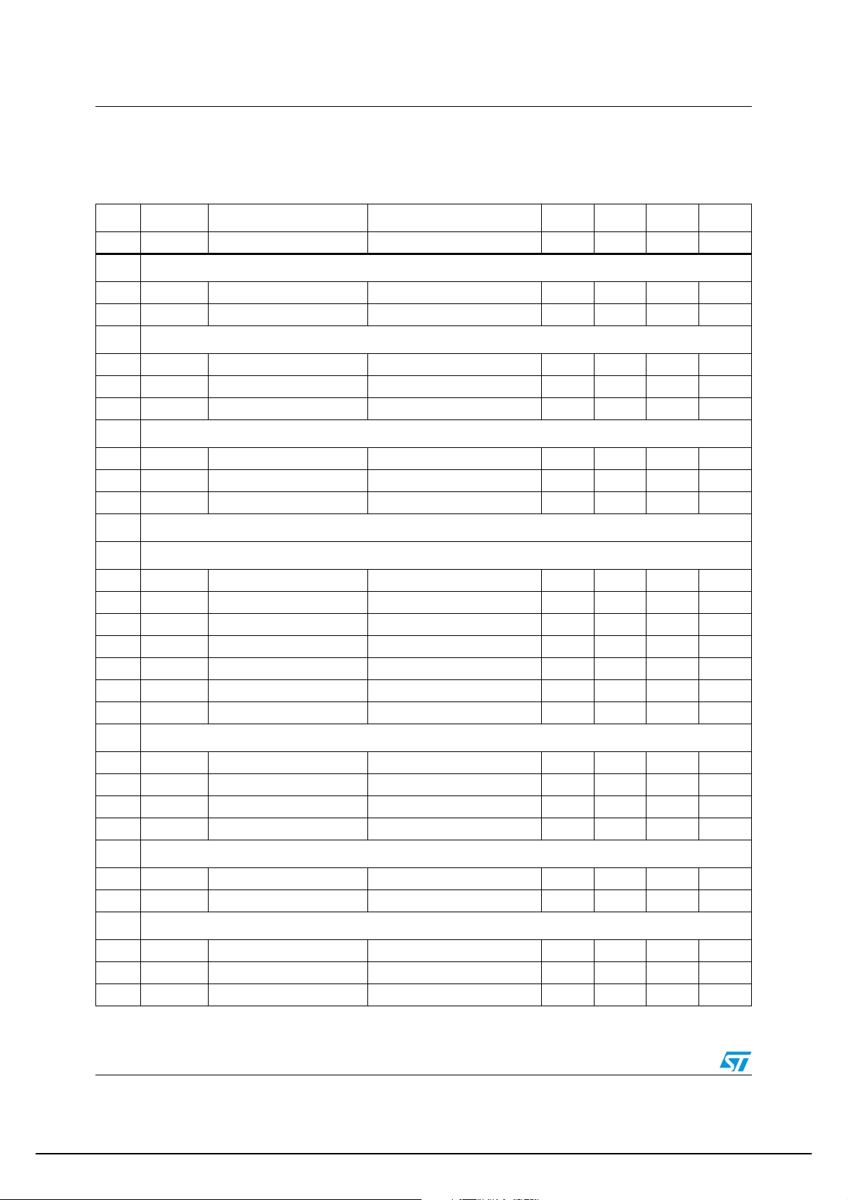
DOCUMENT CD00108485 REVISION 1.0 ACTIVE DATE 11-May-2006 page: 10/75
Electrical specifications TDA7540B
Table 5. Electrical characteristics (continued)
(T
= 25°C, V
amb
f
= 98MHz, dev= 40kHz, f
RF
CC1
= V
CC2
= V
MOD
= V
CC3
= 1kHz, f
= V
CCST
CCVCO
= 10.25MHz, in application circuit, unless
Xtal
= V
CCMIX1
= V
CCMIX2
= V
CCIF1
= 8.5V,
otherwise specified).
Item Symbol Parameter Test Conditions Min. Typ. Max. Unit
5.7 C
Input capacitance 2.5 pF
IN
6 AGC Time Constant Output
V
6.1 V
6.2 V
6.3 I
6.4 I
Max. AGC output voltage V
16
Min. AGC output voltage V
16
Min. AGC charge current V
16
Max. AGC discharge
16
current
V
9-11
9-11
9-11
9-11
= 0mV
= 50mV
= 0mV
= 50mV
RMS
RMS
RMS,V16
RMS,V16
= 2.5V -12.5 µA
= 2.5V 1.25 mA
REF1
+V
BE
0.5 V
V
7 AGC PIN Diode Driver Output
7.1 I
7.2 I
AGC OUT, current min. V
8
AGC OUT, current max. V
8
9-11
9-11
= 0mV
= 50 mV
, V8 = 2.5V 50 µA
RMS
, V8 = 2.5V -20 mA
RMS
8 I/Q Mixer1 (10.7MHz)
8.1 R
8.2 C
8.3 R
8.4 V
8.5 g
OUT
9,11
Input resistance differential 10 kΩ
IN
Input capacitance differential 4 pF
IN
Output resistance differential 100 kΩ
Input dc bias 3.2 V
Conversion
m
transconductance
17 ms
8.6 F Noise figure 400Ω generator resistance 3 dB
8.7 CP
1dB compression point referred to diff. mixer input 100 dBµV
1dB
8.8 IIP3 3rd order intermodulation 122 dBµV
8.9 IQP I/Q phase adjust PH -7 +8 °
8.10 IRR Image rejection ratio ratio wanted/image 30 40 dB
8.11 IRR Image rejection ratio with phase adjust 40 46 dB
9 IF1 Amplifier1 +2 (10.7MHz)
9.1 G2 Gain 6 dB
9.2 G1
9.3 G1
9.4 R
9.5 R
9.6 CP
OUT
Min. gain IFG1 9 dB
min
Max. gain IFG1 18 dB
max
Input resistance 330 W
IN
Output resistance 330 W
1dB compression point referred to 330Ω input 105 dBµV
1dB
9.7 IIP3 3rd order Intermodulation ref. to 330Ω input, 9dB gain 126 dBµV
10 Mixer2 (450kHz)
10.1 R
10.2 V
Input impedance 330 Ω
IN
Max. input voltage 119 dBµV
65
10/75
Copyright STMicroelectronics COMPANY INTERNAL Unauthorized reproduction and communication strictly prohibited
DOCUMENT CD00108485 REVISION 1.0 ACTIVE DATE 11-May-2006 page: 11/75
TDA7540B Electrical specifications
Table 5. Electrical characteristics (continued)
(T
= 25°C, V
amb
f
= 98MHz, dev= 40kHz, f
RF
CC1
= V
CC2
= V
MOD
= V
CC3
= 1kHz, f
= V
CCST
CCVCO
= 10.25MHz, in application circuit, unless
Xtal
= V
CCMIX1
= V
CCMIX2
= V
CCIF1
= 8.5V,
otherwise specified).
Item Symbol Parameter Test Conditions Min. Typ. Max. Unit
10.3 V
Limiting sensitivity S/N = 20dB 28 dBµV
65
10.4 G Mixer gain 18 dB
11 Limiter 1 (450kHz)
11.1 G
Limiter
Gain 80 dB
12 Demodulator, Audio Output
12.1 THD
12.2 V
12.3 R
MPX
OUT
12.4 |∆V|
12.5 |∆V|
12.6 S/N
12.7 V
MPXW
Dev.= 75kHz, V
10mV
RMS
MPX output signal Dev.= 75kHz 500 mV
Output impedance 50 Ω
DC offset fine adjust DEM, MENA=1 8.5 mV
min
DC offset fine adjust DEM, MENA=1 264 mV
max
Dev.= 40kHz,V65 =
10mV
RMS
MPXW output signal Dev.= 75kHz 350 mV
=
65
0.1 %
RMS
76 dB
RMS
13 Quality Detection
S-meter, Unweighted Fieldstrength
13.1 V
13.2 V
13.3 V
13.4 ∆V
13.5 ∆V
13.6 ∆V
13.7 R
OUT
Min. input voltage MIX2 30 dBµV
65
Fieldstrength output V65 = 20dBµV0.1V
22
Fieldstrength output V65 = 119dBµV4.9V
22
voltage per decade SMSL = 0 1 V
22
voltage per decade SMSL = 1 1.5 V
22
S-meter offset SL, SMSL=1 -15 15 dB
22
Output impedance 400 Ω
13.8 TK Temp coeff. 0 ppm/K
Adjacent Channel Gain
13.9 G
13.10 G
max
Gain minimum ACG=0 32 dB
min
Gain maximum ACG=1 38 dB
Adjacent Channel Filter
13.11 f
13.12 f
13.13 f
HP
BP
-20dB
-3dB frequency highpass ACF=0 100 kHz
Centre frequency ACF=1 100 kHz
Attenuation 20dB 70 kHz
Adjacent Channel Output
13.14 V
13.15 V
Output voltage low 0.1 V
23
Output voltage high 4.9 V
23
11/75
Copyright STMicroelectronics COMPANY INTERNAL Unauthorized reproduction and communication strictly prohibited
DOCUMENT CD00108485 REVISION 1.0 ACTIVE DATE 11-May-2006 page: 12/75
Electrical specifications TDA7540B
Table 5. Electrical characteristics (continued)
(T
= 25°C, V
amb
f
= 98MHz, dev= 40kHz, f
RF
CC1
= V
CC2
= V
MOD
= V
CC3
= 1kHz, f
= V
CCST
CCVCO
= 10.25MHz, in application circuit, unless
Xtal
= V
CCMIX1
= V
CCMIX2
= V
CCIF1
= 8.5V,
otherwise specified).
Item Symbol Parameter Test Conditions Min. Typ. Max. Unit
13.16 R
OUT
Output resistance 4 kΩ
Multipath Channel Gain
13.17 G
13.18 G
max
Gain minimum MPG=0 12 dB
min
Gain maximum MPG=1 23 dB
Multipath Bandpass Filter
13.19 f
13.20 f
BP19
BP31
Centre frequency MPF=0 19 kHz
Centre frequency MPF=1 31 kHz
13.21 Q Quality factor 5 8 10
Multipath Output
13.22 V
13.23 V
13.24 R
OUT
Output voltage low 0.1 V
24
Output voltage high 4.9 V
24
Output resistance 2.5 kΩ
14 ISS (intelligent Selectivity System)
Filter 450kHz
14.1 f
centre
Centre frequency f
REF_intern
= 450kHz 450 kHz
14.2 BW 3dB Bandwidth, -3dB ISS80 = 1 80 kHz
14.3 BW 20dB Bandwidth, -20dB ISS80 = 1 150 kHz
14.4 BW 3dB Bandwidth, -3dB ISS80 = 0 120 kHz
14.5 BW 20dB Bandwidth, -20dB ISS80 = 0 250 kHz
14.6 BW 3dB Bandwidth weather band ISS30 = 1 30 kHz
14.7 BW 20dB -20dB weather band ISS30 = 1 80 kHz
Adjacent Channel ISS Filter Threshold
14.8 V
14.9 V
14.10 V
14.11 V
NTH
NTH
WTH
WTH
Internal low threshold ACNTH 0 V
Internal high threshold ACNTH 0.3 V
Internal low threshold ACWTH 0.25 V
Internal high threshold ACWTH 0.95 V
Multipath Threshold
14.12 V
14.13 V
THMP
THMP
Internal low threshold MPTH 0.50 V
Internal high threshold MPTH 1.25 V
ISS Filter Time Constant
14.14 I
14.15 I
14.16 I
27,I28
27,I28
27,I28
Charge current low mid TISS, ISSCTL = 1 -74 µA
Charge current high mid TISS, ISSCTL = 1 -60 µA
Charge current low narrow TISS, ISSCTL = 1 -124 µA
12/75
Copyright STMicroelectronics COMPANY INTERNAL Unauthorized reproduction and communication strictly prohibited
DOCUMENT CD00108485 REVISION 1.0 ACTIVE DATE 11-May-2006 page: 13/75
TDA7540B Electrical specifications
Table 5. Electrical characteristics (continued)
(T
= 25°C, V
amb
f
= 98MHz, dev= 40kHz, f
RF
CC1
= V
CC2
= V
MOD
= V
CC3
= 1kHz, f
= V
CCST
CCVCO
= 10.25MHz, in application circuit, unless
Xtal
= V
CCMIX1
= V
CCMIX2
= V
CCIF1
= 8.5V,
otherwise specified).
Item Symbol Parameter Test Conditions Min. Typ. Max. Unit
14.17 I
14.18 I
14.19 I
27,I28
27,I28
27,I28
Charge current high
narrow
Discharge current low TISS, ISSCTL = 0 1 µA
Discharge current high TISS, ISSCTL = 0 15 µA
TISS, ISSCTL = 1 -110 µA
14.20 V27,V28Low voltage ISSCTL = 0 0.1 V
14.21 V
27,V28
High voltage ISSCTL = 1 4.9 V
ISS Filter Switch Threshold
14.22 V
27,V28
Threshold ISS on ISSCTL = 0 3 V
14.23 V27,V28Threshold ISS off ISSCTL = 0 1 V
14.24 V
14.25 V
27,V28
27,V28
14.26 I
14.27 I
14.28 I
14.29 I
14.30 DEV
14.31 DEV
14.32 RATIO
14.33 RATIO
Threshold ISS narrow on ISSCTL = 0 4 V
Threshold ISS narrow off ISSCTL = 0 2 V
Charge current low TDEV -25 µA
3
Charge current high TDEV -39 µA
3
Discharge current low TDEV 1 µA
3
Discharge current high TDEV 15 µA
3
Internal low threshold DWTH 30 kHz
WTH
Internal high threshold DWTH 75 kHz
WTH
Referred to threshold DTH 1
min
Referred to threshold DTH 1.5
max
15 Softmute
15.1 V
15.2 V
15.3 a
15.4 a
15.5 a
15.6 V
15.7 a
15.8 I
15.9 I
ANT
ANT
SMmin
SMmax
SMTHISS
ACTH
SMAC
49
49
16 S/N MPX
16.1 (S+N)/N
Upper startpoint SMTH, SMD, SLOPE = 0 10 dBµV
lower startpoint SMTH, SMD, SLOPE = 0 3 dBµV
Min. softmute depth
Max. softmute depth
Mute depth threshold for
ISS filter on
Internal AC mute
threshold
SMD, SLOPE = 0,
SMTH
Upper
SMD, SLOPE = 0,
SMTH
Upper
18 dB
36 dB
SMCTH 0.2 1 2 dB
ACM 60 340 mV
AC mute depth ACMD 4 10 dB
Charge current -47.5 µA
Discharge current 2.5 µA
= 60dBµV,
V
ANT
dev.= 40kHz,LP=15KHz
deemphasis t = 50
µs
66 69 dB
13/75
Copyright STMicroelectronics COMPANY INTERNAL Unauthorized reproduction and communication strictly prohibited
DOCUMENT CD00108485 REVISION 1.0 ACTIVE DATE 11-May-2006 page: 14/75
Electrical specifications TDA7540B
3.2.3 AM section
Table 6. Electrical Characteristics
(T
= 25°C, V
amb
= 98MHz, m= 30%, f
f
RF
otherwise specified).
Item Symbol Parameter Test Conditions Min. Typ. Max. Unit
17 Global
CC1
= V
CC2
MOD
= V
= V
CC3
CCST
= 400kHz, f
= V
CCVCO
= 10.25MHz, in application circuit, unless
Xtal
= V
CCMIX1
= V
CCMIX2
= V
CCIF1
= 8.5V,
17.1 V
17.2
17.3 (S+N)/N Signal to Noise Ratio Ref.: V
17.4 a
17.5 f
17.6 THD Total Harmonic Distortion
17.7 V
17.8 V
17.9 V
17.10 V
17.11 V
17.12 |I
Usable sensitivity (S+N)/N = 26 dB 25 19 dBµV
ANT_us
∆V
AF
78max
IF2 AGC Range Ref.: V
ANT
IF rejection
IF
Frequency response
AF output level V
53
IF output level V
24
Min. RF AGC threshold
4
Max. RF AGC threshold
Min. IF AGC threshold
71
Max. IF AGC threshold
Min. DAGC threshold
71
Max. DAGC threshold
Ref: V
IF = 10.7MHz
Ref.: V
∆V
AF
V
INRF
m = 0.3
V
INRF
m = 0.3
INRF
INRF
WAGC
WAGC
DAGC
= 60dBµV, 50 52 dB
INRF
= 60dBµV5055 dB
INRF
= 60dBµV,
INRF
70 80 dB
= 60dBµV,
INRF
= -3 dB
= 60dBµV, m = 0 . 8
3.6 kHz
0.5
0.3
= 120 dBµV, m = 0 . 8
1.0
0.3
= 60dBµV 190 mV
= 60dBµ, m=off 190 mV
90
109
90
109
74
96
| AGC2 charge current seek 160 µA
17.13 CCR Charge current ratio seek/seek off 30
%
RMS
RMS
dBµV
dBµV
dBµV
dBµV
dBµV
dBµV
18 AGC Voltage Driver Output
18.1 V
18.2 V
18.3 | I
Max. AGC output voltage 3.5 V
6
Min. AGC output voltage 0.5 V
6
| AGC current 100 µA
6
19 AGC PIN Diode Driver Output
19.1 I
AGC driver current -2 mA
7
20 AM Mixer1 (10.7MHz)
20.1 R
20.2 C
20.3 R
OUT
Input resistance differential 100 kΩ
IN
Input capacitance differential 4 pF
IN
Output impedance differential 100 kΩ
14/75
Copyright STMicroelectronics COMPANY INTERNAL Unauthorized reproduction and communication strictly prohibited
DOCUMENT CD00108485 REVISION 1.0 ACTIVE DATE 11-May-2006 page: 15/75
TDA7540B Electrical specifications
Table 6. Electrical Characteristics
(T
= 25°C, V
amb
f
= 98MHz, m= 30%, f
RF
CC1
= V
CC2
MOD
= V
= V
CC3
CCST
= 400kHz, f
= V
CCVCO
= 10.25MHz, in application circuit, unless
Xtal
= V
CCMIX1
= V
CCMIX2
= V
CCIF1
= 8.5V,
otherwise specified).
Item Symbol Parameter Test Conditions Min. Typ. Max. Unit
20.4 CP
1dB compression point referred to diff. mixer input 112 dBµV
1dB
20.5 IIP3 3rd order intermodulation 132 dB
20.6 F Noise figure 8 dB
20.7 A Gain 26 dB
20.8 C
20.9 C
20.10 C
min
max
1-80
Min. capacitance step IF1T 0.55 pF
Max. capacitance IF1T 8.25 pF
IF1T 2 pF
21 AM Mixer2 (450kHz)
21.1 R
21.2 C
21.3 CP
Input resistance 330 W
71
Input capacitance 2.5 pF
71
1dB compression point referred to diff. mixer input 120 dBµV
1dB
21.4 IIP3 3rd order intermodulation 132 dBµV
21.5 F Noise figure 12 dB
21.6 A Max. gain Mixer2 tank output 34 dB
21.7 ∆A Gain control range 20 dB
21.8 C
21.9 C
21.10 C
min
max
62-63
Min. cap step IF2T 1.6 pF
Max. cap IF2T 24 pF
IF2T 2 pF
22 IF Noise Blanking
µV
22.1 t
22.2 t
22.3 V
22.4 V
22.5 V
22.6 V
22.7 V
bl
bl
th
th
thstep
desth
desth
Min. blanking time 8 µs
Max. blanking time 17 µs
Min internal threshold 0 mV
Max. internal threshold 187.5 mV
Threshold step 12.5 mV
Min. desensitivity threshold 3.2 V
Max. desensitivity threshold 4 V
15/75
Copyright STMicroelectronics COMPANY INTERNAL Unauthorized reproduction and communication strictly prohibited
DOCUMENT CD00108485 REVISION 1.0 ACTIVE DATE 11-May-2006 page: 16/75
Electrical specifications TDA7540B
3.2.4 Stereodecoder
Table 7. Electrical characteristics
(T
= 25°C, V
amb
= 500mV
V
MPX
circuit, unless otherwise specified).
Item Symbol Parameter Test Conditions Min. Typ. Max. Unit
23 Stereodecoder
= V
CC1
mono, f = 1kHz, deemphasis = 50µs, f
rms
CC2
= V
CC3
= V
CCST
= V
CCVCO
= V
CCMIX1
Xtal
= V
CCMIX2
= 10.25MHz, in application
= V
CCIF1
= 8.5V,
23.1 V
23.2 R
23.3 G
23.4 G
23.5 G
min
max
step
23.6 SVRR
23.7 a Max. channel separation
MPX input level STD Gain = 2,5 dB 0.5 0.93 V
in
Input resistance 100 kΩ
in
Min. Stereodecoder gain 0 dB
Max. Stereodecoder gain 3.75 dB
Stereodecoder gain step
resolution
Supply voltage ripple
rejection
Vripple = 100mV, f = 1kHz 60 dB
V
MPX
= 500mV
rms
stereo
only L/R
1.25 dB
50 dB
23.8 THD Total harmonic distortion 0.02 0.3 %
23.9 (S+N)/N
23.10 V
23.11 R
23.12 V
23.13 V
puafs
puafs
TH1
TH2
Signal plus Noise to Noise
ratio
A-weighted, 19kHz notch 85 dB
Pull up voltage for AFS pin 3.3 V
Pull up resistor for AFS pin 25 kΩ
1. threshold for AFS PIN 2.4 V
2. threshold for AFS PIN 0.8 V
24 Mono/Stereo-switch
24.1 V
24.2 V
24.3 V
24.4 V
PTHST1
PTHST0
PTHMO1
PTHMO0
Pilot threshold voltage for Mono->Stereo, PTH = 1 10 mV
Pilot threshold voltage for Mono->Stereo, PTH = 0 14 mV
Pilot threshold voltage for Stereo->Mono, PTH = 1 8 mV
Pilot threshold voltage for Stereo->Mono, PTH = 0 12 mV
25 19kHz PLL
rms
rms
rms
rms
rms
25.1 f
lock
PLL lock range
Pilot magnitude
20 mV
rms
= 4%
18.9 19.1 kHz
25.2 DP Pilot deviation Pilot frequency 19kHz 4 30 %
26 Deemphasis- and highcut
26.1 t
26.2 t
HC50
HC75
Deemphasis time constant
Deemphasis time constant
DEEMP = 0, DESFT = 1
V
>> V
LEVEL
HCH
DEEMP = 1, DESFT = 1
>> V
V
LEVEL
HCH
50 µs
75 µs
16/75
Copyright STMicroelectronics COMPANY INTERNAL Unauthorized reproduction and communication strictly prohibited
DOCUMENT CD00108485 REVISION 1.0 ACTIVE DATE 11-May-2006 page: 17/75
TDA7540B Electrical specifications
Table 7. Electrical characteristics (continued)
(T
V
amb
MPX
= 25°C, V
= 500mV
= V
CC1
mono, f = 1kHz, deemphasis = 50µs, f
rms
CC2
= V
CC3
= V
CCST
= V
CCVCO
= V
CCMIX1
Xtal
= V
CCMIX2
= 10.25MHz, in application
= V
CCIF1
= 8.5V,
circuit, unless otherwise specified).
Item Symbol Parameter Test Conditions Min. Typ. Max. Unit
26.3 t
26.4 t
26.5 t
26.6 t
26.7 F
26.8 F
HC25
HC37
HC50
HC75
AMCMin
AMCMin
Deemphasis time constant
Deemphasis time constant
Highcut time constant
Highcut time constant
Min. AM corner frequency
Max. AM corner frequency
DEEMP = 0, DESFT = 0
V
LEVEL
DEEMP = 1, DESFT = 0
V
LEVEL
DEEMP = 0, DESFT = 1
V
LEVEL
DEEMP= 1, DESFT = 1
V
LEVEL
DEEMP = 0, DESFT = 1
AMCF
DEEMP = 0, DESFT = 1
AMCF
27 Stereoblend- and highcut-control
27.1 L
27.2 L
27.3 L
Gmin
Gmax
Gstep
27.4 VSBL
27.5 VSBL
27.6 VSBL
27.7 VHCH
27.8 VHCH
27.9 VHCH
27.10 VHCL
27.11 VHCL
27.12 VHCL
Min. level gain LG 0 dB
Max. level gain LG 4.7 dB
Level gain step resolution LG 0.67 dB
Min. voltage for mono SBC 29 %V
min
Max. voltage for mono SBC 58 %V
max
Step resolution SBC 4.2 %V
step
Min. voltage for no highcut VHCH 42 %V
min
Max. Voltage for no highcut VHCH 66 %V
max
Step resolution VHCH 8 %V
step
Min. voltage for full high cut VHCL, MAXHC = 00 11 %VHCH
min
Max. voltage for full high cut VHCL, MAXHC = 00 33 %VHCH
max
Step resolution VHCL, MAXHC = 00 7.3 %VHCH
step
28 Carrier and harmonic suppression at the output
>> V
>> V
<< V
<< V
HCH
25 µs
37.5 µs
HCH
150 µs
HCL
225 µs
HCL
1.06 kHz
3.18 kHz
REF1
REF1
REF1
REF1
REF1
REF1
28.1 a19 Pilot signal f=19kHz V
pilot
= 50mV
rms
50 dB
28.2 a38 Subcarrier f=38kHz 75 dB
28.3 a57 Subcarrier f=57kHz 62 dB
28.4 a76 Subcarrier f=76kHz 90 dB
29 Intermodulation (Note 1)
29.1 a2 f
29.2 a3 f
=10kHz, f
mod
=13kHz, f
mod
=1kHz 65 dB
spur
=1kHz 75 dB
spur
17/75
Copyright STMicroelectronics COMPANY INTERNAL Unauthorized reproduction and communication strictly prohibited
DOCUMENT CD00108485 REVISION 1.0 ACTIVE DATE 11-May-2006 page: 18/75
Electrical specifications TDA7540B
Table 7. Electrical characteristics (continued)
(T
V
amb
MPX
= 25°C, V
= 500mV
= V
CC1
mono, f = 1kHz, deemphasis = 50µs, f
rms
CC2
= V
CC3
= V
CCST
= V
CCVCO
= V
CCMIX1
Xtal
= V
CCMIX2
= 10.25MHz, in application
= V
CCIF1
= 8.5V,
circuit, unless otherwise specified).
Item Symbol Parameter Test Conditions Min. Typ. Max. Unit
30 Traffic Radio (Note 2)
30.1 a57 Signal f=57kHz 70 dB
31 SCA - Subsidiary Communications Authorization (Note 3)
31.1 a67 Signal f=67kHz 75 dB
32 ACI - Adjacent Channel Interference (Note 4)
32.1 a114 Signal f=114kHz 95 dB
32.2 a190 Signal f=190kHz 84 dB
33 FM noise blanker
33.1 V
33.2 V
33.3 V
33.4 V
33.5 V
33.6 V
33.7 V
33.8 V
33.9 V
33.10 V
33.11 V
TRMIN
TRMAX
TRSTEP
TRNOISE
TRNOISE
PEAK
PEAK
PEAK
PEAKDEV
PEAKDEV
PEAKFS
Min. trigger threshold
Max. trigger threshold
Trigger threshold step
Min. noise controlled
trigger threshold
Max. noise controlled
trigger threshold
Peak voltage NBRR = 00, V
Peak voltage V
Peak voltage V
Min. deviation dependent
peak voltage
Max. deviation dependent
peak voltage
Min. fieldstrength controlled
peak voltage
Max. fieldstrength
33.12 V
PEAKFS
controlled
peak voltage
33.13 T
33.14 T
33.15 SR
PEAK
Min. blanking time
S
Max. blanking time
S
Noise rectifier charge
0)
0)
0)
0)
V
=0.8V, NBLTH 147 mV
PEAK
0)
V
=0.8V, NBLTH 280 mV
PEAK
V
=1.5V, NBCTH 450 mV
PEAK
V
=1.5V, NBCTH 1200 mV
PEAK
=50mV, f=150kHz 1.9 V
MPX
=200mV, f=150kHz 3.5 V
MPX
V
=500mV, NBDTH = 11
MPX
V
=500mV, NBDTH= 00 2.0 V
MPX
V
=0mV, V
MPX
(fully mono), NBFS = 11
=0mV, V
V
MPX
(fully mono), NBFS = 00
Signal HOLDN in testmode,
NBT
Signal HOLDN in testmode,
NBT
Signal PEAK in testmode,
NBPC=0
19 mV
=0mV 0.8 V
MPX
0.8
(off)
LEVEL
<< V
SBL
0.8
(off)
<< V
LEVEL
SBL
2.0 V
22 µs
38 µs
10 mV/µs
OP
OP
OP
OP
OP
V
OP
OP
V
33.16 SR
PEAK
Noise rectifier charge
Signal PEAK in testmode,
NBPC=1
20 mV/µs
18/75
Copyright STMicroelectronics COMPANY INTERNAL Unauthorized reproduction and communication strictly prohibited

DOCUMENT CD00108485 REVISION 1.0 ACTIVE DATE 11-May-2006 page: 19/75
TDA7540B Electrical specifications
Table 7. Electrical characteristics (continued)
(T
V
amb
MPX
= 25°C, V
= 500mV
= V
CC1
mono, f = 1kHz, deemphasis = 50µs, f
rms
CC2
= V
CC3
= V
CCST
= V
CCVCO
= V
CCMIX1
Xtal
= V
CCMIX2
= 10.25MHz, in application
= V
CCIF1
= 8.5V,
circuit, unless otherwise specified).
Item Symbol Parameter Test Conditions Min. Typ. Max. Unit
33.17 V
33.18 V
33.19 V
33.20 V
33.21 V
RECTADJ
RECTADJ
RECTADJ
RECTADJ
ADJMP
Noise rectifier discharge
adjustment
Noise rectifier discharge
adjustment
Noise rectifier discharge
adjustment
Noise rectifier discharge
adjustment
Noise rectifier adjustment
by multipath
Noise rectifier adjustment
33.22 V
ADJMP
by strong multipath
influence
Noise rectifier adjustment
33.23 V
ADJMP
by multipath and strong
multipath influence
33.24 G
AMdelay
AM delay filter attenuation f = 2.2kHz 2 dB
34 Multipath Detector
Signal PEAK in testmode,
NBRR=00, NBSMP=0,
MPPC=0
Signal PEAK in testmode,
NBRR=01, NBSMP=0,
MPPC=0
Signal PEAK in testmode,
NBRR=10, NBSMP=0,
MPPC=0
Signal PEAK in testmode,
NBRR=11, NBSMP=0,
MPPC=0
Signal PEAK in testmode,
=1V, NBSMP=0,
V
MPTC
MPPC=1
Signal PEAK in testmode,
V
=1V,, NBSMP=1,
MPTC
MPPC=0
Signal PEAK in testmode,
V
=1V,, NBSMP=1,
MPTC
MPPC=1
0.3 V/ms
0.8 V/ms
1.3 V/ms
2.0 V/ms
TBD V/ms
TBD V/ms
TBD V/ms
34.1 f
34.2 G
34.3 G
34.4 G
34.5 G
34.6 I
34.7 I
34.8 I
CMP
BPMP
BPMP
RECTMP
RECTMP
CHMP
CHMP
DISMP
Center frequency of
multipath-bandpass
Min. band pass gain MPBPG 6 dB
Max. band pass gain MPBPG 12 dB
Min. rectifier gain MPRG 0 dB
Max. rectifier gain MPRG 7.6 dB
Rectifier charge current MPCC = 0 0.8 µA
Rectifier charge current MPCC = 1 0.4 µA
Rectifier discharge current 1 mA
stereo decoder locked on
pilot tone
19 kHz
35 Quality detector
35.1 a Min. MP influence factor QDC 0.6
35.2 a Max. MP
influence factor QDC 1.05
35.3 A Min. noise influence factor QNG 6 dB
35.4 A Max. noise influence factor QNG 15 dB
19/75
Copyright STMicroelectronics COMPANY INTERNAL Unauthorized reproduction and communication strictly prohibited

DOCUMENT CD00108485 REVISION 1.0 ACTIVE DATE 11-May-2006 page: 20/75
Electrical specifications TDA7540B
1. Intermodulation Suppression
a
2 = VO(signal,@1KHz) / VO(spurious, @1KHz) ; fs = (2x10KHz) - 19KHz
a
3 = VO(signal,@1KHz) / VO(spurious, @1KHz) ; fs = (3x13KHz) - 38KHz
measured with: 91% stereo signal; 9% pilot signal; fm = 10kHz or 13kHz.
2. Traffic Radio (V.F.) Suppression
57(V,W,F) = VO(signal,@1KHz) / VO(spurious, @1KHz+/-23KHz)
a
measured with: 91% stereo signal; 9% pilot signal; fm=1kHz; 5% sub carrier (f=57kHz,
fm=23Hz AM, m=60%)
3. SCA ( Subsidiary Communications Authorization )
67 = VO(signal,@1KHz) / VO(spurious, @9KHz) ; fs = (2x38KHz) - 67KHz
a
measured with: 81% mono signal; 9% pilot signal; fm=1kHz; 10%SCA – sub carrier ( fS =
67kHz, unmodulated ).
4. ACI ( Adjacent Channel Interference )
a
114 = VO(signal,@1KHz) / VO(spurious, @4KHz) ; fs = 110KHz - (3x38KHz)
a
190 = VO(signal,@1KHz) / VO(spurious, @4KHz) ; fs = 186KHz - (5x38KHz)
measured with: 90% mono signal; 9% pilot signal; fm=1kHz; 1% spurious signal ( fS =
110kHz or 186kHz, unmodulated).
0
) All thresholds are measured inTestmode at the quality output. The thresholds are
calculated by
V
- V
NBTH
V
PEAK
PEAK
is adjusted by applying a 150kHz sinewave at MPXIN.
20/75
Copyright STMicroelectronics COMPANY INTERNAL Unauthorized reproduction and communication strictly prohibited

DOCUMENT CD00108485 REVISION 1.0 ACTIVE DATE 11-May-2006 page: 21/75
TDA7540B Electrical specifications
Figure 3. Trigger threshold vs. V
VTH
Min. Trig. T hreshold
200 mV
8 STEPS
147 mV
0.8 V
PEAK
Noise Controlled Tr ig. Threshold
Figure 4. Deviation controlled trigger adjustment
V
PEAK
[V ]
OP
1200 mV (00)
950 mV (01)
700 mV (10)
450 mV (11)
V
Peak1.5 V
2.0
1.5
1.0
0.8
20 32.5 45 75
Figure 5. Field strength controlled trigger adjustment
V
PEAK
MONO STEREO
≈
3V
2.0V (00 )
1.6V ( 01)
NOIS E
ATC _SB OF F (11)
1.4V ( 10)
00
01
10
11
Detector off
DEVIATION [KHz]
0.8V
noisy sig nal go od signal
E'
21/75
Copyright STMicroelectronics COMPANY INTERNAL Unauthorized reproduction and communication strictly prohibited

DOCUMENT CD00108485 REVISION 1.0 ACTIVE DATE 11-May-2006 page: 22/75
Electrical specifications TDA7540B
3.2.5 PLL section
Table 8. Electrical characteristics
(T
= 25°C, V
amb
= 98MHz, dev. = 40kHz, f
f
RF
otherwise specified).
Item Symbol Parameter Test Conditions Min. Typ. Max. Unit
36 Output of Tuning Voltages (TV1,TV2)
CC1
= V
CC2
= V
MOD
= V
CC3
= 1kHz, f
CCST
= V
CCVCO
= 10.25MHz, in application circuit, unless
Xtal
= V
CCMIX1
= V
CCMIX2
= V
CCIF1
= 8.5V,
36.1 V
36.2 R
36.3 R
OUT
OUT
OUT
Output voltage TVO 0.5 V
-0.5 V
CC3
Output impedance TVMODE=0 40 kΩ
Output impedance TVMODE=1 20 kΩ
37 Xtal Reference Oscillator
37.1 f
37.2 C
37.3 C
LO
Step
max
37.4 ∆f/f Deviation versus VCC2
Reference frequency C
= 15pF 10.25 MHz
Load
Min. cap step XTAL 0.75 pF
Max. cap XTAL 23.25 pF
∆V
= 1V 1.5 ppm/V
CC2
37.5 ∆f/f Deviation versus temp -40°C < T < +85°C 0.2 ppm/K
38 Loop Filter Input/Output
38.1 -I
38.2 I
38.3 V
38.4 V
38.5 I
38.6 I
IN
IN
OL
OH
OUT
OUT
Input leakage current VIN = GND, PD
= VREF1
V
Input leakage current
Output voltage Low I
Output voltage High I
Output current, sink V
Output current, source V
IN
= Tristate
PD
OUT
= -0.2mA 0.05 0.5 V
OUT
= 0.2mA
OUT
= 1V to V
OUT
= 1V to V
OUT
= Tristate -0.1 0.1 µA
OUT
-0.1 0.1 µA
-
V
V
CC3
0.5
-1V 10 mA
CC3
-1V -10 mA
CC3
CC3
0.05
V
39 Voltage Controlled Oscillator (VCO)
39.1 f
39.2 f
VCOmin
VCOmax
39.3 C/N Carrier to Noise
Minimum VCO frequency 50 MHz
Maximum VCO frequency 260 MHz
= 200MHz, ∆f=1KHz,
f
VCO
B=1Hz, closed loop
80 dBc
40 SSTOP, INLOCK, ISSSTATUS Outputs (Open Collector)
40.1 V Output voltage low I = -200
µA0.20.5V
40.2 V Output voltage high 5 V
40.3 -I Output leakage current V = 5V -0.1 0.1 µA
40.4 I Output current, sink V = 0.5V-5V 1 mA
41 Switching Outputs S1, S2 (Open Collector SMODE=1)
41.1 V Output voltage low I = -5mA 0.2 0.5 V
22/75
Copyright STMicroelectronics COMPANY INTERNAL Unauthorized reproduction and communication strictly prohibited

DOCUMENT CD00108485 REVISION 1.0 ACTIVE DATE 11-May-2006 page: 23/75
TDA7540B Electrical specifications
Table 8. Electrical characteristics (continued)
(T
= 25°C, V
amb
f
= 98MHz, dev. = 40kHz, f
RF
CC1
= V
CC2
= V
MOD
= V
CC3
= 1kHz, f
CCST
= V
CCVCO
= 10.25MHz, in application circuit, unless
Xtal
= V
CCMIX1
= V
CCMIX2
= V
CCIF1
= 8.5V,
otherwise specified).
Item Symbol Parameter Test Conditions Min. Typ. Max. Unit
41.2 V Output voltage high V
CC1
V
41.3 -I Output leakage current V = 5V -3 3 µA
41.4 I Output current, sink V = 0.5V-V
CC
5mA
42 Switching Outputs S1, S2 (Open Emitter SMODE=0)
42.1 V Output voltage low I = 0µA0V
V
-
42.2 V Output voltage high I = 1mA
CC1
1
V
42.3 -I Output leakage current -0.1 0.1 µA
42.4 I Output current, sink V = 5V 5 mA
23/75
Copyright STMicroelectronics COMPANY INTERNAL Unauthorized reproduction and communication strictly prohibited

DOCUMENT CD00108485 REVISION 1.0 ACTIVE DATE 11-May-2006 page: 24/75
Functional description TDA7540B
4 Functional description
4.1 FM section
4.1.1 Mixer1, AGC and 1.IF
FM quadrature I/Q-mixer converts FM RF to IF1 of 10.7MHz. The mixer provides inherent
image rejection and wide dynamic range with low noise and large input signal performance.
The mixer1 tank can be adjusted by software (IF1T). For accurate image rejection the
phase-error of I/Q can be compensated by software (PH)
It is capable of tuning the US FM, US weather, Europe FM, Japan FM and East Europe FM
bands
– US FM = 87.9 to 107.9 MHz
– US weather = 162.4 to 162.55 MHz
– Europe FM = 87.5 to 108 MHz
– Japan FM = 76 to 91 MHz
– East Europe FM = 65.8 to 74 MHz
The AGC operates on different sensitivities and bandwidths in order to improve the input
sensitivity and dynamic range. AGC thresholds are programmable by software
(RFAGC,IFAGC,KAGC). The output signal is a controlled current for pin diode attenuator.
A 10.7MHz programmable amplifier (IFG1) correct the IF ceramic insertion loss and the
costumer level plan application.
4.1.2 Mixer2, limiter and demodulator
In this 2nd mixer stage the first 10.7MHz IF is converted into the second 450kHz IF. A multistage limiter generates signals for the complete integrated demodulator including spike
cancellation (DNB). MPX output DC offset versus noise DC level is correctable by software
(DEM), if tuner softmute is activated.
4.1.3 Quality detection and ISS
Fieldstrength
Parallel to mixer2 input a 10.7MHz limiter generates a signal for digital IF counter and a
fieldstrength output signal. This internal unweighted fieldstrength is used for keying AGC,
adjacent channel and multipath detection and is available at PIN22 (FSU) after +6dB buffer
stage. It is possible to combinate the IF counter result with this FSU via programmable
comparator (SSTH). The behaviour of FSU signal can be corrected for DC offset (SL) and
slope (SMSL). The generated unweighted fieldstrength is externally filtered and used for
softmute function and generation of ISS filter switching signal for weak input level (sm).
Adjacent channel detector
The input of the adjacent channel detector is AC coupled from internal unweighted
fieldstrength. A programmable highpass or bandpass (ACF) and amplifier (ACG) as well as
rectifier determines the influences. This voltage is compared with adjustable comparator1
thresholds (ACWTH, ACNTH). The output signal of this comparator generates a DC level at
PIN27 by programmable time constant. Time control (TISS) for a present adjacent channel
24/75
Copyright STMicroelectronics COMPANY INTERNAL Unauthorized reproduction and communication strictly prohibited

DOCUMENT CD00108485 REVISION 1.0 ACTIVE DATE 11-May-2006 page: 25/75
TDA7540B Functional description
is made by charge and discharge current after comparator1 in an external capacitance. The
charge current is fixed and the discharge current is controlled by I
2
C Bus. This level
produces digital signals (ac, ac+) in an additional comparator4. The adjacent channel
information is available as analog output signal after rectifier and +8dB output buffer.
Multipath detector
The input of the multipath detector is AC coupled from internal unweighted fieldstrength. A
programmable bandpass (MPF) and amplifier (MPG) as well as rectifier determines the
influences. This voltage is compared with an adjustable comparator2 thresholds (MPTH).
The output signal of this comparator2 is used for the "Milano" effect. In this case the
adjacent channel detection is switched off. The "Milano" effect is selectable by I
2
C Bus
(MPOFF). The multipath information is available as analog output signal after rectifier and
+8dB output buffer.
450kHz IF narrow bandpass filter (ISS filter)
The device gets an additional 450KHz IF narrow bandpass filter for suppression of noise
and adjacent channel signal influences. This narrow filter has three switchable bandwidthes,
narrow range of 80kHz, mid range of 120kHz and 30KHz for weather band information.
Without ISS filter the IF bandwidth (wide range) is defined only by ceramic filter chain. The
filter is located between mixer2 and 450kHz limiter stage. The centre frequency is matched
to the demodulator center frequency.
Deviation detector
In order to avoid distortion in audio output signal the narrow ISS filter is switched OFF for
present overdeviation. Hence the demodulator output signal is detected. A lowpass filtering
and peak rectifier generates a signal that is defined by software controlled current (TDEV) in
an external capacitance.
This value is compared with a programmable comparator3 thresholds (DWTH, DTH) and
generates two digital signals (dev, dev+). For weak signal condition deviation threshold is
dependent on FSWO.
ISS switch logic
All digital signals coming from adjacent channel detector, deviation detector and softmute
are acting via switching matrix on ISS filter switch. The IF bandpass switch mode is
controlled by software (ISSON, ISS30, ISS80, CTLOFF). The switch ON of the IF bandpass
is also available by external manipulation of voltage at PIN27. Two application modes are
available (APPM).
The conditions are described in table 51.
4.1.4 Soft mute control
The filtered fieldstrength (FSWO) signal is the reference for mute control. The startpoint and
mute depth are programmable (SMTH, SMD) in a wide range. The time constant is defined
by external capacitance. Additional adjacent channel mute function is supported. A
highpass filter with -3dB threshold frequency of 100kHz, amplifier and peak rectifier
generates an adjacent noise signal from MPX output with the same time constant for
softmute. This value is compared with comparator5 thresholds (ACM). For present strong
adjacent channel the MPX signal is additional attenuated (ACMD).
25/75
Copyright STMicroelectronics COMPANY INTERNAL Unauthorized reproduction and communication strictly prohibited

DOCUMENT CD00108485 REVISION 1.0 ACTIVE DATE 11-May-2006 page: 26/75
Functional description TDA7540B
4.2 AM section
The up/down conversion is combined with gain control circuit sensing three input signals,
narrow band information at PIN 54, upconversion signal (IF2AGC) at PIN 71and wide band
information (RFAGC) at PIN 4.This gain control gives two output signals. The first one is a
current for pin diode attenuator and the second one is a voltage for preamplifier. Time
constant of RF- and IF-AGC is defined by internal 100k resistor and external capacitor at
PIN 67. The intervention points for AGC (DAGC,WAGC) are programmable by software.
In order to avoid a misbehaviour of AGC intervention point it is important to know that the
DAGC threshold has to be lower than WAGC threshold !
The oscillator frequency for upconversion-mixer1 is generated by dividing the VCO
frequency after VCO divider (VCOD) and AM predivider(AMD).
Two 10,7MHz ceramic filters before mixer2 input increases 900KHz attenuation.In mixer2
the IF1 is down converted into the IF2 450kHz. After filtering by ceramic filter a 450kHz
amplifier is included with an additional gain control of IF2 below DAGC threshold. Time
constant is defined by capacitance at PIN 78.
Mixer1 and mixer2 tanks are software controlled adjustable (IF1T, IF2T).
The demodulator is a peak detector to generate the audio output signal.
A separate output is available for AMIF stereo (AMST).
AM IF noise blanker
In order to remove in AM short spikes a noise cancellation conception is used in 450KHz IF
AM level. The advantage is to avoid long narrow AGC- and demodulator- time constants,
wich enlarge spike influences on audio signal and makes difficult to remove it in audio path.
The 10,7MHz AM IF signal generates before 10,7 MHz ceramic filter via limitation an
unweighted fieldstrenght signal including slope of noise spike. The comparison of these
detected slope between fast and slow rectifier ignores audio modulation whereby the
threshold of slow rectifier is programmable (AINBT). A comparator activates a pulse
generator.
The duration of this pulse is software programmable (AINT) and is smooth blanking out the
spikes in 450KHz AM mixer2. Additionally this funtionality is controlled by narrow AM
fieldstrenght (AINBD).
4.3 Stereodecoder
4.3.1 Decoder
The stereo decoder-part of the TDA7540 (see Fig. 14) contains all functions necessary to
demodulate the MPX-signal like pilot tone-dependent MONO/STEREO-switching as well as
"stereoblend" and "highcut". Adaptations like programmable input gain, roll-off
compensation, selectable deemphasis time constant and a programmable field strength
input allow easy adaption to different applications.
The 4.th order input filter has a corner frequency of 80kHz and is used to attenuate spikes
and noise and acts as an anti-aliasing filter for the following switch capacitor filters.
26/75
Copyright STMicroelectronics COMPANY INTERNAL Unauthorized reproduction and communication strictly prohibited

DOCUMENT CD00108485 REVISION 1.0 ACTIVE DATE 11-May-2006 page: 27/75
TDA7540B Functional description
Demodulator
In the demodulator block the left and the right channel are separated from the MPX-signal.
In this stage also the 19-kHz pilot tone is canceled. For reaching a high channel separation
the TDA7540 offers an I2C-bus programmable roll-off adjustment, which is able to
compensate the low pass behavior of the tuner section. Within the compensation range an
adjustment to obtain at least 40dB channel separation is possible. The bits for this
adjustment are located together with the level gain adjustment in one byte. This gives the
possibility to perform an optimization step during the production of the car radio where the
channel separation and the field strength control are trimmed.
In addition to that the FM signal can be inverted.
Deemphasis and Highcut
The deemphasis low pass allows to choose between a time constant of 50µs/ 75µs
(DEEMP) and 25µs/37.5µs (DESFT). The highcut control range will be in both cases τ
2xτ
. Inside the highcut control range (between VHCH and VHCL) the LEVEL signal is
Deemp
converted into a 5-bit word, which controls the low pass time constant between
τ
Deemp
...3xτ
. Thereby the resolution will remain always 5 bits independently of the
Deemp
absolute voltage range between the VHCH- and VHCL-values.
The highcut function can be switched off by I
2
C-bus .
HC
=
In AM mode (AMON = 1) the bits DEEMP and DESFT together with the AM corner
frequency bits (AMCF1...5) can be used as programmable AM frequency response. The
maximum corner frequency is defined by τ
, the minimum is defined by 3xτ
Deemp
Deemp
19kHz PLL and pilot tone detector
The PLL has the task to lock on the 19kHz pilot tone during a stereo-transmission to allow a
correct demodulation. The included pilot tone-detector enables the demodulation if the pilot
tone reaches the selected pilot tone threshold
V
. Two different thresholds are available.
PTHST
By reading the status byte of the TDA7540 via I2C-bus the detector output can be checked.
Field Strength Control
The field strength input is used to control the highcut- and the stereoblend-function. In
addition the signal can be also used to control the noise blanker thresholds and as input for
the multipath detector.
LEVEL-Input and -Gain
As level input for the stereo decoder is used the FSU voltage (pin22). Appling a capacitor at
FSTC (pin33) a desired time constant can by reached together with the internal resistor of
10k between FSU pin and FSTC pin.
In addition to that the LEVEL signal is low pass filtered internally in order to suppress
undesired high frequency modulation on the highcut- and stereoblend-function . The filter is
a combination of a 1.st-order RC-low pass at 53kHz (working as anti-aliasing filter) and a
1.st-order switched capacitor low pass at 2.2kHz. The second stage is a programmable gain
stage to adapt the LEVEL signal internally . The gain is widely programmable in 8 steps
from 0dB to 4,7dB (step=0.67dB). These 3bits are located together with the Roll-Off bits in
the "Stereo decoder 8"-byte to simplify a possible adaptation during the production of the
car radio.
27/75
Copyright STMicroelectronics COMPANY INTERNAL Unauthorized reproduction and communication strictly prohibited

DOCUMENT CD00108485 REVISION 1.0 ACTIVE DATE 11-May-2006 page: 28/75
Functional description TDA7540B
Stereoblend control
The stereoblend control block converts the internal LEVEL-voltage into a demodulator
compatible analog signal, which is used to control the channel separation between 0dB and
the maximum separation. Internally this control range has a fixed upper limit, which is the
internal reference voltage
V
in 4% steps (see fig.6).
REF1
To adjust the external LEVEL-voltage to the internal range two values must be defined: the
LEVEL gain
L
and VSBL. To adjust the voltage where the full channel separation is reached
G
(VST) the LEVEL gain
the gain:
The MONO-voltage VMO (0dB channel separation) can be chosen selecting VSBL.
Figure 6. Relation between internal and external level-voltagees and setup of stereoblend
V
. The lower limit can be programmed between 29 and 58% of
REF1
L
has to be defined. The following equation can be used to estimate
G
L
G
= V
/FSU@full stereo
REF1
The stereo blend function can be switched ON/OFF using bit Addr25<d2>. Please note that
in AM it must be switched in forced mono!
Highcut control
The highcut control set-up is similar to the stereoblend control set-up: the starting point
VHCH can be set with 2 bits to be 42, 50, 58 or 66% of
whereas the range can be set
VREF1
to be 11, 18.3, 25.7 or 33% of VHCH (see fig. 7).
28/75
Copyright STMicroelectronics COMPANY INTERNAL Unauthorized reproduction and communication strictly prohibited

L
ass
t
imeconstan
t
V
V
ieldstrengt
h
t
DOCUMENT CD00108485 REVISION 1.0 ACTIVE DATE 11-May-2006 page: 29/75
TDA7540B Functional description
Figure 7. Highcut characteristics
owp
3
•
D eem p
D eem p
HCL
HC HF
4.3.2 Functional description of the noise blanker
In the automotive environment spikes produced by the ignition or for example the wipermotor disturb the MPX-signal. The aim of the noise blanker part is to cancel the audible
influence of the spikes. Therefore the output of the stereo decoder is held at the actual
voltage for a time between 22
blanker is given in fig.15.
In a first stage the spikes must be detected but to avoid a wrong triggering on high
frequency (white) noise a complex trigger control is implemented. Behind the trigger stage a
pulse former generates the "blanking"-pulse. An own biasing circuit supplies the noise
blanker in order to avoid any cross talk to the signal path.
Trigg er pa th
The incoming MPX signal is high pass filtered, amplified and rectified. This second order
high pass filter has a corner-frequency of 140kHz. The rectified signal, RECT, is low pass
filtered to generate a signal called PEAK. Also noise with a frequency 140kHz increases the
PEAK voltage. The resulting voltage can be adjusted by use of the noise rectifier discharge
current. The PEAK voltage is fed to a threshold generator, which adds to the PEAK-voltage
a DC-dependent threshold VTH. Both signals, RECT and PEAK+VTH are fed to a
comparator, which triggers a re-triggerable monoflop. The monoflop's output activates the
sample-and-hold circuits in the signal path for the selected duration.
µs and 38µs (programmable). The block diagram of the noise
Automatic noise controlled threshold adjustment (see Figure 3)
There are mainly two independent possibilities for programming the trigger threshold:
1. the low threshold in 8 steps (NBLTH)
2. and the noise adjusted threshold in 4 steps (NBCTH).
The low threshold is active in combination with a good MPX signal without any noise; the
PEAK voltage is less than 1V. The sensitivity in this operation is high.
If the MPX signal is noisy (low fieldstrength) the PEAK voltage increases due to the higher
noise, which is also rectified. With increasing of the PEAK voltage the trigger threshold
increases, too. This particular gain is programmable in 4 steps (NBCTH).
29/75
Copyright STMicroelectronics COMPANY INTERNAL Unauthorized reproduction and communication strictly prohibited

DOCUMENT CD00108485 REVISION 1.0 ACTIVE DATE 11-May-2006 page: 30/75
Functional description TDA7540B
Automatic threshold control by the stereoblend voltage (see Figure 5)
Besides the noise controlled threshold adjustment there is an additional possibility for
influencing the noise blanker trigger threshold using the bits NBFS. This influence depends
on the stereoblend control.
The point where the MPX signal starts to become noisy is fixed by the RF part. This point is
also the starting point of the normal noise-controlled trigger adjustment. But in some cases
the noise blanker can create a wrong triggering, which create distortion, already in the
region of mono/stereo transition. Therefore a opportunity to control the PEAK voltage by the
stereo blend function it is implemented.
Over deviation detector (see Figure 4)
If the system is tuned to stations with a high deviation the noise blanker can trigger on the
higher frequencies of the modulation. To avoid this wrong behavior, which causes noise in
the output signal, the noise blanker offers a deviation-dependent threshold adjustment. By
rectifying the MPX signal a further signal representing the actual deviation is obtained. It is
used to increase the PEAK voltage. Offset and gain of this circuit are programmable in 3
steps (NBDTH) of the stereo decoder-byte (the first step turns off the detector).
Multipath-level
To react on high repetitive spikes caused by a Multipath-situation, the discharge-time of the
PEAK voltage can be decreased depending on the voltage-level at Pin MPout. There are
two ways to do this. One way is to switch on the linear influence of the Multipath-Level on the
PEAK-signal . In this case the discharge slew rate is 1V/ms
(a)
. The second possibility is to
activate a function, which switches to the 18k discharge if the Multipath-Level is below 2.5V.
AM mode of noise blanker
The TDA7540 offers an AM audio noise blanker too.
If the AM noise blanker is used the AM audio delay filter must be switched on. It is not
recommented to use the AM noise blanker without to use the AMIF noiseblanker inside the
tuner.
Together with the IF AM moise blanker, this audio noise blanking can work in two different
modes.
Mode 1 uses the same threshold controls like in FM mode. The detector uses in AM mode
the audio input for spike detection. A combination of programmable gain stage and low pass
filtering forms an envelope detector wich drives the noise blanker input via 10/20KHz,
1st/2nd order high pass filter.
In mode 2 only a fixed noise blanker threshold is used.
In order to blank the whole spike in AM mode the hold time of the S&H circuit is much longer
than in FM mode (640µs -1,2ms)
4.3.3 Functional description of the multipath-detector
Using the internal Multipath-Detector the audible effects of a multipath condition can be
minimized. A multipath-condition is detected by rectifying the 19kHz spectrum in the
fieldstrength signal. An external capacitor is used to define the attack- and decay-times (see
a. The slew rate is measured with RDischarge=infinite and VMPout=2.5V
30/75
Copyright STMicroelectronics COMPANY INTERNAL Unauthorized reproduction and communication strictly prohibited

DOCUMENT CD00108485 REVISION 1.0 ACTIVE DATE 11-May-2006 page: 31/75
TDA7540B Functional description
block diagram, fig. 16). The MP_OUT-pin is used as detector-output connected to a
capacitor of about 47nF. Using this configuration an external adaptation to the user's
requirement is possible without affecting the "normal" fieldstrength input (LEVEL) for the
stereo decoder.
To keep the old value of the Multipath Detector during an AF-jump, the MP-Hold switch can
disconnect the external capacitor. This switch is controlled directly by the AFS-Pin.
Selecting MPION the channel separation is automatically reduced during a multipath
condition according to the voltage appearing at the MP_OUT-pin.
Programming
To obtain a good multipath performance an adaptation is necessary. Therefore the gain of
the first 19kHz-bandpass is programmable in two steps (MPG), the gain of the second
19kHz-bandpass is programmable in four steps (MPBPG) and the rectifier gain is
programmable in four steps(MPRG). Please note that the frequency of the first multipath
bandpass (MPF) must be set to 19kHz! The attack- and decay-times can be set by the
external capacitor value and the multipath detector charge current MPCC.
4.3.4 Quality detector
The TDA7540 offers a quality detector output, which gives a voltage representing the FMreception conditions. To calculate this voltage the MPX-noise and the multipath-detector
output are summed according to the following formula:
V
= 0.8b (V
Qual
-0.8 V)+ a (V
Noise
The noise-signal is the PEAK-signal without additional influences (see noise blanker
description). The factor 'a' can be programmed from 0.6 to 1.05(QDC) and the factor b can
be programmed from 6dB to 15dB ( QNG). The output is a low impedance output able to
drive external circuitry as well as simply fed to an AD-converter for RDS applications.
4.3.5 AFS control and stereo decoder mute
The TDA7540 is supplied with several functionality to support AF-checks using the stereo
decoder. The additional pin (AFS) is implemented in order to speed up the stereo decoder
AF-functions compared to IIC controlling.
The block diagramm of AFS function is shown in Figure 17.
In order to separate the different functions of the AFS pin, two different logic thresholds are
implemented. Below the higher threshold voltage (2.4V) only the multipath-detector is
switched into small time constant (internal logical signal MPfast).
Below the lower threshold voltage (0.8V) the full AFS function is activated. The MPXIN pin is
switched into high impedance mode (internal signal AFSMute), which avoids any clicks
during the jump condition. If the stereo decoder is not muted, it is possible at the same time
to evaluate the noise- and multipath-content of the alternate frequency using the Quality
detector output.
REF1-VMpout
).
Furthermore the AFS pin does also freeze the condition of pilot locking and magnitude
(internal signal PDhold). The Pdhold signal is defined by V
th1
or V
, dependent on the
th2
PDH signal.
31/75
Copyright STMicroelectronics COMPANY INTERNAL Unauthorized reproduction and communication strictly prohibited

DOCUMENT CD00108485 REVISION 1.0 ACTIVE DATE 11-May-2006 page: 32/75
Functional description TDA7540B
4.4 PLL and if counter section
4.4.1 PLL frequency synthesizer block
This part contains a frequency synthesizer and a loop filter for the radio tuning system. Only
one VCO is required to build a complete PLL system for FM world tuning and AM
upconversion (see Figure 9). For auto search stop operation an IF counter system is
available.
The PLL counter works in a two stages configuration. The first stage is a swallow counter
with a two modulus (32/33) precounter. The second stage is an 11-bit programmable
counter.
The circuit receives the scaling factors for the programmable counters and the values of the
reference frequencies via an I
2
C-Bus interface.The reference frequency is generated by an
adjustable internal (XTAL) oscillator followed by the reference divider. The main reference
and step-frequencies are free selectable (RC, PC).
Output signals of the phase detector are switching the programmable current sources. The
loop filter integrates their currents to a DC voltage.
The values of the current sources are programmable by 6 bits also received via the I
2
C Bus
(A, B, CURRH, LPF).
To minimize the noise induced by the digital part of the system, a special guard
configuration is implemented.
The loop gain can be set for different conditions by setting the current values of the
chargepump generator.
Frequency generation for phase comparison
The RF signals applies a two modulus counter (32/33) pre-scaler, which is controlled by a 5bit A-divider. The 5-bit register (PC0 to PC4) controls this divider. In parallel the output of the
prescaler connects to an 11-bit B-divider. The 11-bit PC register (PC5 to PC15) controls this
divider
Dividing range behind VCO divider:
f
= [33 x A + (B + 1 - A) x 32] x f
VCOdiv
f
= (32 x B + A + 32) x f
VCOdiv
REF
Important: For correct operation: A ≤ 32; B ≥ A
REF
Three state phase comparator
The phase comparator generates a phase error signal according to phase difference
between f
SYN
and f
. This phase error signal drives the charge pump current generator.
REF
Charge pump current generator
This system generators signed pulses of current. The phase error signal decides the
duration and polarity of those pulses. The current absolute values are programmable by A
register for high current and B register for low current.
32/75
Copyright STMicroelectronics COMPANY INTERNAL Unauthorized reproduction and communication strictly prohibited

DOCUMENT CD00108485 REVISION 1.0 ACTIVE DATE 11-May-2006 page: 33/75
TDA7540B Functional description
Inlock detector
Switching the chargepump in low current mode can be done either via software or
automatically by the inlock detector, by setting bit LDENA to "1".
After reaching a phase difference about lower than 40nsec the chargepump is forced in low
current mode. A new PLL divider alternation by I
high current mode.
Low noise CMOS op-amp
An internal voltage divider at pin VREF2 connects the positive input of the low noise opamp. The charge pump output connects the negative input. This internal amplifier in
cooperation with external components can provide an active filter. The negative input is
switchable to three input pins, to increase the flexibility in application. This feature allows two
separate active filters for different applications.
While the high current mode is activated LPHC output is switched on.
4.4.2 IF counter block
The aim of IF counter is to measure the intermediate frequency of the tuner for AM and FM
mode. The input signal for FM and AM upconversion is the same 10.7MHz IF level after
limiter. AM 450KHz signal is coming from narrow filtered IF2 before demodulation. A switch
controlled by IF counter mode (IFCM) is choosing the input signal for IF counter.
The grade of integration is adjustable by eight different measuring cycle times. The
tolerance of the accepted count value is adjustable, to reach an optimum compromise for
search speed and precision of the evaluation.
The IF-counter mode
2
C-Bus will switch the chargepump in the
The IF counter works in 3 modes controlled by IFCM register.
Sampling timer
A sampling timer generates the gate signal for the main counter. The basically sampling
time are in FM mode 6.25kHz (t
=160µs) and in AM mode 1kHz (t
TIM
=1ms). This is
TIM
followed by an asynchronous divider to generate several sampling times.
Intermediate frequency main counter
This counter is a 11 - 21-bit synchronous autoreload down counter. Five bits (CF) are
programmable to have the possibility for an adjust to the centre frequency of the IF-filter.
The counter length is automatic adjusted to the chosen sampling time and the counter mode
(FM, AM-UPC, AM).
At the start the counter will be loaded with a defined value which is an equivalent to the
divider value (t
SamplexfIF
If a correct frequency is applied to the IF counter frequency input at the end of the sampling
time the main counter is changing its state from 0h to 1FFFFFh.
).
33/75
Copyright STMicroelectronics COMPANY INTERNAL Unauthorized reproduction and communication strictly prohibited

DOCUMENT CD00108485 REVISION 1.0 ACTIVE DATE 11-May-2006 page: 34/75
Functional description TDA7540B
This is detected by a control logic and an external search stop output is changing from LOW
to HIGH. The frequency range inside which a successful count result is adjustable by the
EW bits.
t
= (CF + 1696+1) / fIFFM mode
CNT
t
= (CF + 10688+1) / fIFAM up conversion mode
CNT
t
= (CF + 488+1) / f
CNT
IF
AM mode
Counter result succeeded:
t
≥ t
≤ t
CNT
CNT
- t
+ t
ERR
ERR
TIM
t
TIM
Counter result failed:
t
> t
TIM
t
< t
TIM
t
= IF timer cycle time (sampling time)
TIM
t
CNT
t
ERR
+ t
CNT
CNT
- t
ERR
ERR
= IF counter cycle time
= discrimination window (controlled by the EW registers)
The IF counter is only started by inlock information from the PLL part. It is enabled by
software (IFENA).
Adjustment of the measurement sequence time
The precision of the measurements is adjustable by controlling the discrimination window.
This is adjustable by programming the control registers EW.
The measurement time per cycle is adjustable by setting the registers IFS.
Adjust of the Frequency Value
The center frequency of the discrimination window is adjustable by the control registers CF.
4.5 I2C-Bus interface
The TDA7540 supports the I2C-Bus protocol. This protocol defines any device that sends
data onto the bus as a transmitter, and the receiving device as the receiver. The device that
controls the transfer is a master and device being controlled is the slave. The master will
always initiate data transfer and provide the clock to transmit or receive operations.
4.5.1 Data transition
Data transition on the SDA line must only occur when the clock SCL is LOW. SDA transitions
while SCL is HIGH will be interpreted as START or STOP condition.
4.5.2 Start condition
A start condition is defined by a HIGH to LOW transition of the SDA line while SCL is at a
stable HIGH level. This "START" condition must precede any command and initiate a data
transfer onto the bus. The device continuously monitors the SDA and SCL lines for a valid
START and will not response to any command if this condition has not been met.
34/75
Copyright STMicroelectronics COMPANY INTERNAL Unauthorized reproduction and communication strictly prohibited

DOCUMENT CD00108485 REVISION 1.0 ACTIVE DATE 11-May-2006 page: 35/75
TDA7540B Functional description
4.5.3 Stop condition
A STOP condition is defined by a LOW to HIGH transition of the SDA while the SCL line is at
a stable HIGH level. This condition terminates the communication between the devices and
forces the bus-interface of the device into the initial condition.
4.5.4 Acknowledge
Indicates a successful data transfer. The transmitter will release the bus after sending 8 bits
of data. During the 9th clock cycle the receiver will pull the SDA line to LOW level to indicate
it receive the eight bits of data.
4.5.5 Data transfer
During data transfer the device samples the SDA line on the leading edge of the SCL clock.
Therefore, for proper device operation the SDA line must be stable during the SCL LOW to
HIGH transition.
4.5.6 Device addressing
To start the communication between two devices, the bus master must initiate a start
instruction sequence, followed by an eight bit word corresponding to the address of the
device it is addressing.
The most significant 6 bits of the slave address are the device type identifier.
The TDA7540 device type is fixed as "110001".
The next significant bit is used to address a particular device of the previous defined type
connected to the bus.
The state of the hardwired PIN 59 defines the state of this address bit. So up to two devices
could be connected on the same bus. When PIN 59 is connected to VCC2 and a resistor at
PIN 55 versus ground of about 5,6k Ohm the address bit “1” is selected. In this case the AM
part doesn’t work. Otherwise the address bit “0” is selected (FM and AM is working).
Therefor a double FM tuner concept is possible.
The last bit of the start instruction defines the type of operation to be performed:
– When set to "1", a read operation is selected
– When set to "0", a write operation is selected
The TDA7540 connected to the bus will compare their own hardwired address with the slave
address being transmitted, after detecting a START condition. After this comparison, the
TDA7540 will generate an "acknowledge" on the SDA line and will do either a read or a write
operation according to the state of R/W bit.
4.5.7 Write operation
Following a START condition the master sends a slave address word with the R/W bit set to
"0". The device will generate an "acknowledge" after this first transmission and will wait for a
second word (the word address field). This 8-bit address field provides an access to any of
the 64 internal addresses.
Upon receipt of the word address the TDA7540 slave device will respond with an
"acknowledge". At this time, all the following words transmitted to the TDA7540 will be
considered as Data. The internal address will be automatically incremented up to hex40 in
35/75
Copyright STMicroelectronics COMPANY INTERNAL Unauthorized reproduction and communication strictly prohibited

DOCUMENT CD00108485 REVISION 1.0 ACTIVE DATE 11-May-2006 page: 36/75
Functional description TDA7540B
page mode. Than again subaddresse hex60 has to be transmitted for following registers
above 32.
After each word receipt the TDA7540 will answer with an "acknowledge".
4.5.8 Read operation
If the master sends a slave address word with the R/W bit set to "1", the TDA7540 will transit
one 8-bit data word. This data word includes the following informations:
bit0 (ISS filter, 1 = ON, 0 = OFF)
bit1 (ISS filter bandwidth, 1 = 80kHz, 0 = 120kHz)
bit2 (STEREO,1 = STEREO, 0 = MONO)
bit3 (1 = PLL is locked in , 0 = PLL is locked out).
bit4 (fieldstrength indicator, 1 = lower as softmute threshold, 0 = higher as softmute
threshold)
bit5 (adjacent channel indicator, 1 = adjacent channel present, 0 = no adjacent channel)
bit6 (deviation indicator, 1 = strong overdeviation present, 0 = no strong overdeviation)
bit7 (deviation indicator, 1 = overdeviation present, 0 = no overdeviation)
36/75
Copyright STMicroelectronics COMPANY INTERNAL Unauthorized reproduction and communication strictly prohibited

DOCUMENT CD00108485 REVISION 1.0 ACTIVE DATE 11-May-2006 page: 37/75
TDA7540B Software specification
5 Software specification
The interface protocol comprises:
– start condition (S)
– chip address byte
– subaddress byte
– sequence of data (N bytes + Acknowledge)
– stop condition (P)
The pagermode is only working up to byte 31. After byte 31 it is need to send again the chip
address followed by the subaddress 32 and the databytes starting from 32 up to 39!
5.1 Address organization
Table 9. Address organization
FunctionAddr76543210
CHARGEPUMP 0 FMSEEK CURRH B1 B0 A3 A2 A1 A0
PLL COUNTER
TV1 3 TV1O7 TV1O6 TV1O5 TV1O4 TV1O3 TV1O2 TV1O1 TV1O0
TV2 4 TV2O7 TV2O6 TV2O5 TV2O4 TV2O3 TV2O2 TV2O1 TV2O0
IFC CTRL 1 5 LDENA CASF IFCM1 IFCM0 IFENA IFS2 IFS1 IFS0
IFC CTRL 2 6 EW2 EW1 EW0 CF4 CF3 CF2 CF1 CF0
AM CTL 7 LM TVMODE TV2WB TV1WB AMD1 AMD0 AMST AMSEEK
QUALITYISS 8 TISS2 TISS1 TISS0 --- ISS30 ISS80 ISSON CTLOFF
QUALITY AC 9 ACNTH1 ACNTH0 ACWTH2 ACWTH1 ACWTH0 ACG ACF ---
QUALITY MP 10 MPAC APPM2 APPM1 MPTH1 MPTH0 MPG MPF MPOFF
QUALITYDEV 11 BWCTL DTH1 DTH0 DWTH1 DWTH0 TDEV2 TDEV1 TDEV0
1 PC7 PC6 PC5 PC4 PC3 PC2 PC1 PC0
2 PC15 PC14 PC13 PC12 PC11 PC10 PC9 PC8
37/75
Copyright STMicroelectronics COMPANY INTERNAL Unauthorized reproduction and communication strictly prohibited

DOCUMENT CD00108485 REVISION 1.0 ACTIVE DATE 11-May-2006 page: 38/75
Software specification TDA7540B
Table 9. Address organization (continued)
FunctionAddr76543210
MUTE1 12 MENA SMD3 SMD2 SMD1 SMD0 SMTH2 SMTH1 SMTH0
MUTE2 13 F100K ACM3 ACM2 ACM1 ACM0 ACMD1 ACMD0 SMCTH
VCO/PLLREF 14 LPF AMON RC2 RC1 RC0 VCOD2 VCOD1 VCOD0
FMAGC 15 RFKAGC KAGC2 KAGC1 KAGC0 IFAGC1 IFAGC0 RFAGC1 RFAGC0
AMAGC 16 DAGC3 DAGC2 DAGC1 DAGC0 WAGC3 WAGC2 WAGC1 WAGC0
DEM ADJ 17 DNB1 DNB0 DEM5 DEM4 DEM3 DEM2 DEM1 DEM0
LEVEL 18 ODSW ODCUR SMSL SL4 SL3 SL2 SL1 SL0
IF1/XTAL 19 XTAL4 XTAL3 XTAL2 XTAL1 XTAL0 IFG11 IFG10 XTLIM
TANK ADJ 20 IF1T3 IF1T2 IF1T1 IF1T0 IF2T3 IF2T2 IF2T1 IF2T0
I/Q ADJ 21 SMO1 SMO0 --- --- PH3 PH2 PH1 PH0
AMIFNB 22 AINT1 AINT0 AINBD1 AINBD0 AINBT3 AINBT2 AINBT1 AINBT0
SCTRL 23 SSTH3 SSTH2 SSTH1 SSTH0 S2MODE S2 S1MODE S1
STD1 24 STVCO1 STVCO0 NBT1 NBT0 SI TFCKL NBFT TSMA
STD2 25 STING1 STING0 DEEMP PTH NBPC MS STDON STDM
STD3 26 NBDTH1 NBDTH0 NBON NBCTH1 NBCTH0 NBLTH2 NBLTH1 NBLTH0
STD4 27 NBSMP VHCL1 VHCL0 VHCH1 VHCH0 MAXHC1 MAXHC0 HCON
STD5 28 MPPC QDC1 QDC0 NBFS1 NBFS0 SBC2 SBC1 SBC0
STD6 29 MPRG1 MPRG0 MPCC MPION MPBPG1 MPBPG0 NBRR1 NBRR0
STD7 30 AMAF LG2 LG1 LG0 ROC3 ROC2 ROC1 ROC0
STD8 31 AMNBD AMNBFO AMNBHP PDH AFSM AFSON QNG1 QNG0
STD9 32 AMCF4 AMCF3 AMCF2 AMCF1 AMCF0 DESFT --- ---
TESTTU1 33 OUT20 ISSIN TOUT TIN1 CLKSEP TEST3 TEST2 TEST1
TESTTU2 34 OUT7 OUT6 OUT5 OUT4 OUT3 OUT2 OUT1 OUT0
TESTTU3 35 --- TINACM TINMP TINAC OUT11 OUT10 OUT9 OUT8
TESTTU4 36 OUT19 OUT18 OUT17 OUT16 OUT15 OUT14 OUT13 OUT12
TESTTU5 37 TIN2 OUT27 OUT26 OUT25 OUT24 OUT23 OUT22 OUT21
TESTSTD 38 --- --- MUXST3 MUXST2 MUXST1 MUXST0 --- TST
FMDEMSB 39 VCOM PCM --- SBSH SBA SBTO SBW SBT
38/75
Copyright STMicroelectronics COMPANY INTERNAL Unauthorized reproduction and communication strictly prohibited

DOCUMENT CD00108485 REVISION 1.0 ACTIVE DATE 11-May-2006 page: 39/75
TDA7540B Software specification
5.2 Control register function
Table 10. Control register function
Register Name Function
A Charge pump high current
ACF Adjacent channel filter select
ACG Adjacent channel filter gain
ACM Threshold for startpoint adjacent channel mute
ACMD Adjacent channel mute depth
ACNTH Adjacent channel narrow band threshold
ACWTH Adjacent channel wide band threshold
AFSM AFS influence on stereodecoder mute
AFSON AFS Pin enable
AINBD AM IF noise blanker desensitivity
AINBT AM IF noise blanker threshold
AINT AM IF noise blanking time
AMAF AM audio filter
AMD AM prescaler
AMCF AM corner frequency
AMIN AM IF1 input select
AMNBD AM audio delay for noise blanking
AMNBFO AM audio noise blanker high pass filter order
AMNBHP AM audio noise blanker high pass filter frequency
AMON AM-FM switch
AMSEEK Set short time constant of AGC in AM seek mode
AMST AM stereo select
APPM Application mode quality detection
B Charge pump low current
BWCTL ISS filter fixed bandwith (ISS80) in automatic control
CASF Check alternative station frequency
CF Center frequency IF counter
CLKSEP Clock separation (only for testing)
CTLOFF Switch off automatic control of ISS filter
CURRH Set current high charge pump
DAGC AM narrow band AGC threshold
DEEMP Stereodecoder deemphasis
DEM Demodulator offset
39/75
Copyright STMicroelectronics COMPANY INTERNAL Unauthorized reproduction and communication strictly prohibited

DOCUMENT CD00108485 REVISION 1.0 ACTIVE DATE 11-May-2006 page: 40/75
Software specification TDA7540B
Table 10. Control register function (continued)
Register Name Function
DESFT Stereodecoder deemphasis shift
DNB Demodulator spike blanking threshold
DTH Deviation detector threshold for ISS filter “OFF”
DWTH Deviation detector threshold for ISS filter narrow/wide
EW Frequency error window IF counter
F100K Corner frequency of AC-mute high pass filter
FMSEEK ISS time constant change in FM seek mode
HCON High cut enable
IF1T FM/AM mixer1 tank adjust
IF2T AM mixer2 tank adjust
IFAGC FM IF AGC
IFCM IF counter mode
IFENA IF counter enable
IFG IF1 amplifier gain (10.7MHz)
IFS IF counter sampling time
ISSIN Test input for ISS filter
ISSON ISS filter “ON”
ISS30 ISS filter 30KHz weather band
ISS80 ISS filter narrow/mid switch
KAGC FM keying AGC
LDENA Lock detector enable
LG Level gain adjust in stereodecoder
LM Local mode FM seek stop
LPF Loop filter input select
MAXHC Maximum high cut
MENA Softmute enable
MPAC Adjacent channel control by multipath
MPCC Multipath detector charge current
MPBPG Multipath detector bandpass filter gain
MPF Multipath filter frequency
MPG Multipath filter gain
MPION Multipath internal influence enable
MPOFF Multipath control “OFF”
MPPC Multipath influence on peak discharge current
MPRG Multipath detector rectifier gain
40/75
Copyright STMicroelectronics COMPANY INTERNAL Unauthorized reproduction and communication strictly prohibited

DOCUMENT CD00108485 REVISION 1.0 ACTIVE DATE 11-May-2006 page: 41/75
TDA7540B Software specification
Table 10. Control register function (continued)
Register Name Function
MPTH Multipath threshold
MS Mono/Stereo switch automatically
MUXST Test multiplexer output stereodecoder
NBCTH Noise blanker noise controlled threshold
NBDTH Noise blanker deviation controlled threshold
NBFS Field strength controlled noise blanker
NBFT AM noise blanker fixed threshold
NBLTH Noise blanker low threshold
NBON Noise blanker enable
NBPC Noise blanker peak charge current
NBRR Noise blanker rectifier discharge resistor
NBSMP Strong multipath influence on noise blanker on/off
NBT Noise blanker time
ODCUR Current for overdeviation-correction
ODSW Overdeviation-correction enable
OUT Test output (only for testing)
PC Counter for PLL (VCO frequency)
PCM Pilot cancellation mode
PDH PD hold activation
PH I/Q mixer phase adjust
PTH Pilot threshold
QDC Quality detector coefficient
QNG Quality noise gain
RC Reference counter PLL
RFAGC FM RF AGC
RFKAGC FM RF keying AGC
ROC Roll-Off compensation
S Two mode switching output enable
SBA FM demodulator spike blanker attack mode
SBC Stereoblend control
SBSH FM demodulator spike blanker sample&hold mode
SBT FM demodulator spike blanker test mode
SBTO FM demodulator spike blanker toggle mode
SBW FM demodulator spike blanker window mode
SI Signal invertion
41/75
Copyright STMicroelectronics COMPANY INTERNAL Unauthorized reproduction and communication strictly prohibited

DOCUMENT CD00108485 REVISION 1.0 ACTIVE DATE 11-May-2006 page: 42/75
Software specification TDA7540B
Table 10. Control register function (continued)
Register Name Function
SL S meter slider
SMODE Two mode switching output
SMCTH Softmute capacitor threshold for ISS “ON”
SMD Softmute depth threshold
SMO Softmute reference voltage offset
SMSL S meter slope
SMTH Softmute startpoint threshold
SSTH Unweighted fieldstrenght threshold for seek stop
STDON Stereodecoder on/off if muted
STDM Stereodecoder mute enable
STING Stereodecoder ingain
STVCO Stereodecoder VCO adjust
TDEV Time constant for deviation detector
TEST Testing PLL/IFC (only for testing)
TFCKL Fast clock for testing audioprocessor
TIN Switch FSU PIN to TEST input (only for testing)
TINAC Test input adjacent channel (only for testing)
TINACM Test input adjacent channel mute (only for testing)
TINMP Test input multipath(only for testing)
TISS Time constant for ISS filter “ON”/”OFF”
TMSA Test mode stereodecoder and audioprocessor
TOUT Switch FSU PIN to Test output (only for testing)
TST Test stereodecoder enable
TVMODE Tuning voltage offset mode
TVO Tuning voltage offset for prestage
TVWB Tuning voltage offset for prestage (weather band mode)
VCOD VCO divider
VCOM Stereodecoder VCO mode
VHCH Start level high cut
VHCL Stop level high cut
WAGC AM wide band AGC
XTAL Xtal frequency adjust
XTLIM Xtal amplitude limitation
42/75
Copyright STMicroelectronics COMPANY INTERNAL Unauthorized reproduction and communication strictly prohibited

DOCUMENT CD00108485 REVISION 1.0 ACTIVE DATE 11-May-2006 page: 43/75
TDA7540B Software specification
Table 11. Subaddress
MSB LSB
I A5A4A3A2A1A0
000000Charge pump control
-------
100000STD9
-------
100111FMDEMSB
0 Page mode “OFF”
1 Page mode enable
5.2.1 Data Byte Specification
Table 12. Addr 0 Charge Pump Control
MSB LSB
d7 d6 d5 d4 d3 d2 d1 d0
0000High current = 0mA
Function
Function
0001High current = 0.5mA
0010High current = 1mA
0011High current = 1.5mA
-----
1111High current = 7.5mA
0 0 Low current = 0
0 1 Low current = 50
1 0 Low current = 100
1 1 Low current = 150
µA
µA
µA
µA
0 Select low current
1 Select high current
0 ISS time constant at PIN 27 available, FMSEEK “OFF”
1 ISS time constant at PIN 28 available, FMSEEK “ON”
Table 13. Addr 1 PLL Counter 1 (LSB)
MSB LSB
Function
d7 d6 d5 d4 d3 d2 d1 d0
00000000LSB = 0
00000001LSB = 1
00000010LSB = 2
43/75
Copyright STMicroelectronics COMPANY INTERNAL Unauthorized reproduction and communication strictly prohibited

DOCUMENT CD00108485 REVISION 1.0 ACTIVE DATE 11-May-2006 page: 44/75
Software specification TDA7540B
Table 13. Addr 1 PLL Counter 1 (LSB) (continued)
MSB LSB
Function
d7 d6 d5 d4 d3 d2 d1 d0
---------
11111100LSB = 252
11111101LSB = 253
11111110LSB = 254
11111111LSB = 255
Table 14. Addr 2 PLL Counter 2 (MSB)
MSB LSB
d7 d6 d5 d4 d3 d2 d1 d0
00000000MSB = 0
00000001MSB = 256
00000010MSB = 512
---------
11111100MSB = 64768
11111101MSB = 65024
11111110MSB = 65280
11111111MSB = 65536
Swallow mode: f
Table 15. Addr 3,4 TV1,2
VCO/fSYN
= LSB + MSB + 32
MSB LSB
d7 d6 d5 d4 d3 d2 d1 d0
0000000Tuning Voltage Offset = 0
0000001TVO = 25mV
Function
Function
0000010TVO = 50mV
---------
1111111TVO = 3175mV
0-TVO
1+TVO
44/75
Copyright STMicroelectronics COMPANY INTERNAL Unauthorized reproduction and communication strictly prohibited

DOCUMENT CD00108485 REVISION 1.0 ACTIVE DATE 11-May-2006 page: 45/75
TDA7540B Software specification
Table 16. Addr 5 IF Counter Control 1
MSB LSB
d7 d6 d5 d4 d3 d2 d1 d0
000t
001t
010t
011t
100t
101t
110t
111t
0 IF counter disable / stand by
1 IF counter enable
00 Not valid
0 1 IF counter FM mode
1 0 IF counter AM mode (450KHz)
1 1 IF counter AM mode (10.7MHz)
= 20.48ms (FM)128ms (AM )
Sample
= 10.24ms (FM)64ms (AM )
Sample
= 5.12ms (FM)32ms (AM )
Sample
= 2.56ms (FM)16ms (AM )
Sample
= 1.28ms (FM)8ms (AM )
Sample
= 640µs (FM)4ms (AM )
Sample
= 320µs (FM)2ms (AM)
Sample
= 160µs (FM)1ms (AM )
Sample
Function
0 Disable mute & AGC on hold in FM mode
1 Enable mute & AGC on hold in FM mode
0 Lock detector disable
1 Lock detector enable
Table 17. Addr 6 IF Counter Control 2
MSB LSB
d7 d6 d5 d4 d3 d2 d1 d0
00000f
00001f
---------
01011f
01100f
01101f
01110f
01111f
---------
11111f
000 Not valid
= 10.60625MHz (FM) / 10.689MHz ; 449KHz (AM)
Center
= 10.61250MHz (FM) / 10.690MHz ; 450KHz (AM)
Center
= 10.67500MHz (FM) / 10.700MHz ; 460KHz (AM)
Center
= 10.68125MHz (FM) / 10.701MHz ; 461KHz (AM)
Center
= 10.68750MHz (FM) / 10.702MHz ; 462KHz (AM)
Center
= 10.69375MHz (FM) / 10.703MHz ; 463KHz (AM)
Center
= 10.70000MHz (FM) / 10.704MHz ; 464KHz(AM)
Center
= 10.80000MHz (FM) / 10.720MHz ;480KHz (AM)
Center
Function
001 Not valid
45/75
Copyright STMicroelectronics COMPANY INTERNAL Unauthorized reproduction and communication strictly prohibited

DOCUMENT CD00108485 REVISION 1.0 ACTIVE DATE 11-May-2006 page: 46/75
Software specification TDA7540B
Table 17. Addr 6 IF Counter Control 2 (continued)
MSB LSB
Function
d7 d6 d5 d4 d3 d2 d1 d0
010 Not valid
011 ∆f = 6.25kHz (FM)1kHz (AM)
100 ∆f = 12.5kHz (FM) 2kHz (AM)
101 ∆f = 25kHz (FM) 4kHz (AM)
110 ∆f = 50kHz (FM) 8kHz (AM)
111 ∆f = 100kHz (FM)16kHz (AM)
Table 18. Addr 7 AM Control
MSB LSB
d7 d6 d5 d4 d3 d2 d1 d0
0 Multipath information available FM at PIN 24
1 AM stereo output available at PIN 24
0 0 Prescaler ratio 10
0 1 Prescaler ratio 8
1 0 Prescaler ratio 6
1 1 Prescaler ratio 4
0 0 Disable additional TV1, 2 offset
0 1 Enable additional TV1 offset +3,175V (for weather band)
1 0 Enable additional TV2 offset +3,175V (for weather band)
1 1 Enable additional TV1, 2 offset +3,175V (for weather band)
0 TV is tracking with PLL
1 TV is independing on PLL
Function
0 Normal AGC time constant
1 Short time constant for AM seek stop
0 Disable local mode
1 Enable local mode (PIN diode current = 0.5mA)
Table 19. Addr 8 Quality ISS Filter
MSB
LSB
Function
d7 d6 d5 d4 d3 d2 d1 d0
0 ISS filter control “ON”
1 ISS filter control “OFF”
0 Switch ISS filter “OFF”
1 Switch ISS filter “ON”
46/75
Copyright STMicroelectronics COMPANY INTERNAL Unauthorized reproduction and communication strictly prohibited

DOCUMENT CD00108485 REVISION 1.0 ACTIVE DATE 11-May-2006 page: 47/75
TDA7540B Software specification
Table 19. Addr 8 Quality ISS Filter (continued)
MSB
LSB
Function
d7 d6 d5 d4 d3 d2 d1 d0
0 Switch “OFF” ISS filter 120kHz
1 Switch “ON” ISS filter 80kHz
0 Switch “OFF” ISS filter 30KHz for weatherband
1 Switch “ON” ISS filter 30KHz for weatherband
000
001
010
discharge current1µA, charge current mid 74µA
narrow124µA
discharge current3µA, charge current mid 72µA
narrow122µA
discharge current5µA, charge current mid 70µA
narrow120µA
0 1 1 discharge current7µA, charge current mid 68
--- -
111
discharge current15µA,charge current mid
60µAnarrow110µA
Table 20. Addr 9 Quality Detection Adjacent Channel
MSB LSB
Function
d7 d6 d5 d4 d3 d2 d1 d0
ϖ narrow118µA
0/1 Not valid
0 AC highpass frequency 100kHz
1 AC bandpass frequency 100kHz
0 AC gain 32dB
1 AC gain 38dB
0 0 0 AC wide band threshold 0.25V
0 0 1 AC wide band threshold 0.35V
0 1 0 AC wide band threshold 0.45V
--- -
1 1 1 AC wide band threshold 0.95V
0 0 AC narrow band threshold 0.0V
0 1 AC narrow band threshold 0.1V
1 0 AC narrow band threshold 0.2V
1 1 AC narrow band threshold 0.3V
47/75
Copyright STMicroelectronics COMPANY INTERNAL Unauthorized reproduction and communication strictly prohibited

DOCUMENT CD00108485 REVISION 1.0 ACTIVE DATE 11-May-2006 page: 48/75
Software specification TDA7540B
Table 21. Addr 10 Quality Detection Multipath
MSB LSB
Function
d7 d6 d5 d4 d3 d2 d1 d0
0 Multipath control “ON”
1 Multipath control “OFF”
0 MP bandpass frequency 19KHz
1 MP bandpass frequency 31KHz
0 MP gain 12dB
1 MP gain 23dB
0 0 MP threshold 0.50V
0 1 MP threshold 0.75V
1 0 MP threshold 1.00V
1 1 MP threshold 1.25V
0 0 Application mode 1
0 1 Application mode 2
0 Multipath eliminates ac
1 Multipath eliminates ac and ac+
Table 22. Addr 11 Quality Deviation Detection
MSB LSB
d7 d6 d5 d4 d3 d2 d1 d0
0 0 0 charge current 39µA
0 0 1 charge current 37µA
0 1 0 charge current 35µA
0 1 1 charge current 33µA
, discharge current 1µA
, discharge current 3µA
, discharge current 5µA
, discharge current 7µA
----
1 1 1 charge current 25µA
, discharge current 15µA
0 0 DEV threshold for ISS narrow/wide 30kHz
0 1 DEV threshold for ISS narrow/wide 45kHz
1 0 DEV threshold for ISS narrow/wide 60kHz
Function
1 1 DEV threshold for ISS narrow/wide 75kHz
0 0 DEV threshold for ISS filter “OFF” ratio 1.5
0 1 DEV threshold for ISS filter “OFF” ratio 1.4
1 0 DEV threshold for ISS filter “OFF” ratio 1.3
1 1 DEV threshold for ISS filter “OFF” ratio 1
48/75
Copyright STMicroelectronics COMPANY INTERNAL Unauthorized reproduction and communication strictly prohibited

DOCUMENT CD00108485 REVISION 1.0 ACTIVE DATE 11-May-2006 page: 49/75
TDA7540B Software specification
Table 22. Addr 11 Quality Deviation Detection (continued)
MSB LSB
Function
d7 d6 d5 d4 d3 d2 d1 d0
0
1
Disable ISS filter to fixed bandwith (ISS80) in automatic
control
Enable ISS filter to fixed bandwith (ISS80) in automatic
control
Table 23. Addr 12 Softmute Control 1
MSB LSB
Function
d7 d6 d5 d4 d3 d2 d1 d0
0 0 0 Startpoint mute 0 in application about 3dB
0 0 1 Startpoint mute 1 in application about 4dB
----
1 1 1 Startpoint mute 7 in application about 10dBµV antenna level
0 0 0 0 Mute depth 0 in application 18dB
0 0 0 1 Mute depth 1 in application 20dB
0 0 1 0 Mute depth 2 in application 22dB
0 0 1 1 Mute depth 3 in application 24dB
---- - (logarithmically behaviour)
1 1 1 1 Mute depth 15 in application 36dB
0 FM mute disable, (has to be 0 in AM mode)
µV antenna level
µV antenna level
1 FM mute enable
Table 24. Addr 13 Softmute Control 2
MSB LSB
d7 d6 d5 d4 d3 d2 d1 d0
0 Disable mute threshold for ISS filter “ON”
1 Enable mute threshold for ISS filter “ON”
0 0 AC mute depth 10dB
0 1 AC mute depth 8dB
1 0 AC mute depth 6dB
1 1 AC mute depth 4dB
0 0 0 0 AC mute threshold 60mV
0 0 0 1 AC mute threshold 80mV
0 0 1 0 AC mute threshold 100mV
---- -
0 1 1 1 AC mute threshold 340mV
49/75
Function
Copyright STMicroelectronics COMPANY INTERNAL Unauthorized reproduction and communication strictly prohibited

DOCUMENT CD00108485 REVISION 1.0 ACTIVE DATE 11-May-2006 page: 50/75
Software specification TDA7540B
Table 24. Addr 13 Softmute Control 2 (continued)
MSB LSB
Function
d7 d6 d5 d4 d3 d2 d1 d0
1 1 1 1 AC mute “OFF”
0 AC mute filter 110KHz
1 AC mute filter 100KHz
Table 25. Addr 14 VCODIV/PLLREF
MSB LSB
Function
d7 d6 d5 d4 d3 d2 d1 d0
0 0 not valid (only for testing)
0 1 VCO frequency divided by 2
1 0 VCO frequency divided by 3
1 1 original VCO frequency
0 VCO” I” signal 0 degree
1 VCO “I” signal 180 degree
1 0 0 PLL reference frequency 50KHz
1 0 1 PLL reference frequency 25KHz
1 1 0 PLL reference frequency 10KHz
1 1 1 PLL reference frequency 9KHz
0 0 0 PLL reference frequency 2KHz
0 Select FM mode
1 Select AM mode
0 Select PLL low pass filter FM
1 Select PLL low pass filter AM
Table 26. Addr 15 FM AGC
MSB LSB
d7 d6 d5 d4 d3 d2 d1 d0
0 0 RFAGC threshold V
0 1 RFAGC threshold V
1 0 RFAGC threshold V
1 1 RFAGC threshold V
0 0 IFAGC threshold V
0 1 IFAGC threshold V
1 0 IFAGC threshold V
1 1 IFAGC threshold V
9-11TH
9-11TH
9-11TH
9-11TH
77TH
77TH
77TH
77TH
Function
= 85(77 ANT)dBµV
= 90(82 ANT)dBµV
= 94(86 ANT)dBµV
= 96(88 ANT)dBµV
= 86(60 ANT)dBµV
= 92(66 ANT)dBµV
= 96(70 ANT)dBµV
= 98(72 ANT)dBµV
50/75
Copyright STMicroelectronics COMPANY INTERNAL Unauthorized reproduction and communication strictly prohibited

DOCUMENT CD00108485 REVISION 1.0 ACTIVE DATE 11-May-2006 page: 51/75
TDA7540B Software specification
Table 26. Addr 15 FM AGC (continued)
MSB LSB
Function
d7 d6 d5 d4 d3 d2 d1 d0
0 0 0 KAGC threshold 80dBµV
0 0 1 KAGC threshold 82dB
0 1 0 KAGC threshold 84dB
0 1 1 KAGC threshold 86dB
1 0 0 KAGC threshold 88dB
µV
µV
µV
µV
1 0 1 KAGC threshold 90dBµV
1 1 0 KAGC threshold 92dBµV
1 1 1 Keying AGC “OFF”
0RF KAGC“0FF”
1RF KAGC“0N”
Table 27. Addr 16 AM AGC
MSB LSB
Function
d7 d6 d5 d4 d3 d2 d1 d0
0000WAGC V
0001WAGC V
0010WAGC V
0011
WAGC V
ANT)dBµ
0100WAGC V
0101WAGC V
0110
0111
WAGC V
ANT)dBµ
WAGC V
ANT)dBµ
1000WAGC V
1001WAGC V
1010WAGC V
1011
WAGC V
ANT)dBµ
= 90(65 ANT)dBµ V
4TH
= 94(69 ANT)dBµ V
4TH
= 97(72 ANT)dBµ V
4TH
= 98,5(73,5 ANT)dBµ V
4TH
= 100(75 ANT)dBµ V
4TH
= 101,5(76,5 ANT)dBµ V
4TH
= 102,5(77,5 ANT)dBµV
4TH
= 103,5(78,5 ANT)dBµV
4TH
= 104,5(79,5 ANT)dBµ V
4TH
= 105(80 ANT)dBµ V
4TH
= 106(81 ANT)dBµ V
4TH
= 106,5(81,5 ANT)dBµV
4TH
= 90(60 ANT)dBµ
71TH
= 94(64 ANT)dBµ
71TH
= 96,5(66,5 ANT)dBµ
71TH
= 98,5(68,5
71TH
= 100(70 ANT)dBµ
71TH
= 101(71 ANT)dBµ
71TH
= 102,5(72,5
71TH
= 103,5(73,5
71TH
= 104(74 ANT)dBµ
71TH
= 105(75 ANT)dBµ
71TH
= 105,5(75,5 ANT)dBµ
71TH
= 106,5(76,5
71TH
1100WAGC V
1101WAGC V
1110WAGC V
1111WAGC V
0000 DAGC V
= 107(82 ANT)dBµ V
4TH
= 108(83 ANT)dBµ V
4TH
= 108,5(83,5 ANT)dBµ V
4TH
= 109(84 ANT)dBµ V
4TH
= 74(44 ANTENNA)dBµ
71TH
= 107(77 ANT)dBµ
71TH
= 107,5(77,5 ANT)dBµ
71TH
= 108(78 ANT)dBµ
71TH
= 108,5(78,5 ANT)dBµ
71TH
51/75
Copyright STMicroelectronics COMPANY INTERNAL Unauthorized reproduction and communication strictly prohibited

DOCUMENT CD00108485 REVISION 1.0 ACTIVE DATE 11-May-2006 page: 52/75
Software specification TDA7540B
Table 27. Addr 16 AM AGC (continued)
MSB LSB
Function
d7 d6 d5 d4 d3 d2 d1 d0
0001 DAGC V
0010 DAGC V
0011 DAGC V
0100 DAGC V
0101 DAGC V
0110 DAGC V
0111 DAGC V
1000 DAGC V
1001 DAGC V
1010 DAGC V
1011 DAGC V
1100 DAGC V
1101 DAGC V
1110 DAGC V
1111 DAGC V
Table 28. Addr 17 FM Demodulator Fine Adjust
MSB LSB
d7 d6 d5 d4 d3 d2 d1 d0
= 77(47 ANTENNA)dBµ
71TH
= 79(49 ANTENNA)dBµ
71TH
= 80,5(50,5 ANTENNA)dBµ
71TH
= 82(52 ANTENNA)dBµ
71TH
= 83,5(53,5 ANTENNA)dBµ
71TH
= 85(55 ANTENNA)dBµ
71TH
= 86,5(56,5 ANTENNA)dBµ
71TH
= 88(58 ANTENNA)dBµ
71TH
= 89(59 ANTENNA)dBµ
71TH
= 90(60 ANTENNA)dBµ
71TH
= 91(61 ANTENNA)dBµ
71TH
= 92(62 ANTENNA)dBµ
71TH
= 93(63 ANTENNA)dBµ
71TH
= 94(64 ANTENNA)dBµ
71TH
= 96(66 ANTENNA)dBµ
71TH
Function
0000000mV
000001+8.5mV
000010+17mV
-------
011111+263.5mV
1000000mV
100001-8.5mV
100010-17mV
-------
111111-263.5mV
0 0 Spike cancelation ”OFF”
0 1 Threshold for spike cancelation 750mV
1 0 Threshold for spike cancelation 270mV
1 1 Threshold for spike cancelation 520mV
52/75
Copyright STMicroelectronics COMPANY INTERNAL Unauthorized reproduction and communication strictly prohibited

DOCUMENT CD00108485 REVISION 1.0 ACTIVE DATE 11-May-2006 page: 53/75
TDA7540B Software specification
Table 29. Addr 18 S-Meter Slider
MSB LSB
d7 d6 d5 d4 d3 d2 d1 d0
0000S meter slider offset SL=0dB
0001S meter offset SL=1dB
0010S meter offset SL=2dB
-----
1111S meter offset SL=15dB
0 S meter offset -SL
1 S meter offset +SL
0 S Meter slope 1V/decade
1 S meter slope 1.5V/decade
0 Overdeviation correction current max=45µA
1 Overdeviation correction current max=90µA
0 Overdeviation correction “OFF”
1 Overdeviation correction “ON”
Table 30. Addr 19 IF GAIN/XTAL Adjust
Function
MSB LSB
d7 d6 d5 d4 d3 d2 d1 d0
0 Xtal amplitude limitation disable
1 Xtal amplitude limitation enable
0 0 IF1 gain1 9dB
0 1 IF1 gain1 12dB
1 0 IF1 gain1 15dB
1 1 IF1 gain1 18dB
00000 C
00001 C
00010 C
00011 C
00100 C
----- -
11111 C
Load
Load
Load
Load
Load
Load
Function
0pF
0.75pF
1.5pF
2.25pF
3pF
23.25pF
53/75
Copyright STMicroelectronics COMPANY INTERNAL Unauthorized reproduction and communication strictly prohibited

DOCUMENT CD00108485 REVISION 1.0 ACTIVE DATE 11-May-2006 page: 54/75
Software specification TDA7540B
Table 31. Addr 20 Tank Adjust
MSB LSB
d7 d6 d5 d4 d3 d2 d1 d0
0 0 0 0 450kHz 0pF
0 0 0 1 450kHz 1.6pF
0 0 1 0 450kHz 3.2pF
0 0 1 1 450kHz 4.8pF
-----
1 1 1 1 450kHz 24pF
0 0 0 0 10.7MHz 0pF
0 0 0 1 10.7MHz 0.55pF
0 0 1 0 10.7MHz 1.1pF
0 0 1 1 10.7MHz 1.65pF
---- -
1 1 1 1 10.7MHz 8.25pF
Table 32. Addr 21 I/Q FM Mixer1 Adjust
Function
MSB LSB
Function
d7 d6 d5 d4 d3 d2 d1 d0
0000-7 degree
0001-6 degree
0010-5 degree
-----
01110 degree
1000+1 degree
1001+2 degree
-----
1111+8degree
0 0 Softmute reference offset OFF
0 1 Softmute reference offset -50mV
1 0 Softmute reference offset -100mV
1 1 Softmute reference offset -150mV
54/75
Copyright STMicroelectronics COMPANY INTERNAL Unauthorized reproduction and communication strictly prohibited

DOCUMENT CD00108485 REVISION 1.0 ACTIVE DATE 11-May-2006 page: 55/75
TDA7540B Software specification
Table 33. Addr 22 AM IF Noise Blanker
MSB LSB
d7 d6 d5 d4 d3 d2 d1 d0
0000AINBT 0mV
0001AINBT 12.5mV
0010AINBT 25mV
-----
1111AINBT 187.5mV
0 0 AINBD “ON”
0 1 AINBD 4.0V
1 0 AINBD 3.2V
1 1 AINBD “OFF”
00 AINT 8
01 AINT 11
10 AINT 14
11 AINT 17
Table 34. Addr 23 Switch Control
Function
µs
µs
µs
µs
MSB LSB
Function
d7 d6 d5 d4 d3 d2 d1 d0
0 S1 LOW output voltage
1 S1 HIGH output voltage
0 S1 emitter output available
1 S1 open collector output available
0 S2 LOW output voltage
1 S2 HIGH output voltage
0 S2 emitter output available
1 S2 open collector output available
0 0 0 0 SSTOP=IFC (IF counter status)
0 0 0 1 SSTOP= H if IFC=H&FSU>0.89V
0 0 1 0 SSTOP= H if IFC=H&FSU>1.16V
0 0 1 1 SSTOP= H if IFC=H&FSU>1.43V
----
1 1 1 1 SSTOP= H if IFC=H&FSU>4.67V
55/75
Copyright STMicroelectronics COMPANY INTERNAL Unauthorized reproduction and communication strictly prohibited

DOCUMENT CD00108485 REVISION 1.0 ACTIVE DATE 11-May-2006 page: 56/75
Software specification TDA7540B
Table 35. Addr 24 Stereodecoder 1
MSB LSB
Function
d7 d6 d5 d4 d3 d2 d1 d0
0 Test mode stereodecoder and audioprocessor “ON”
1 Test mode stereodecoder and audioprocessor “OFF”
0 Audio AM noise blanker fix threshold disable
1 Audio AM noise blanker fix threshold enable
0 Fast clock for testing audioprocessor “ON”
1 Fast clock for testing audioprocessor “OFF”
0 Audio inverter OFF
1 Audio inverter ON
0 0 Audio noise blanking time (FM = 38µs, AM = 1.2 ms)
0 1 Audio noise blanking time (FM = 25,5µs, AM = 0.8 ms)
1 0 Audio noise blanking time (FM = 32µs, AM = 1.0 ms)
1 1 Audio noise blanking time (FM = 22µs, AM = 0.64 ms)
0 Stereodecoder VCO adjust minus
1 Stereodecoder no VCO adjust
0 Stereodecoder VCO adjust plus
1 Stereodecoder no VCO adjust
Table 36. Addr 25 Stereodecoder 2
MSB LSB
d7 d6 d5 d4 d3 d2 d1 d0
0 Stereo decoder mute disable
1 Stereo decoder mute enable
0 Stereo decoder “ON” if muted
1 Stereo decoder “OFF” if muted
0 Forced MONO, must be set in AM
1 MONO/STEREO switch automatically
0 Noise blanker peak charge current low
1 Noise blanker peak charge current high
0 Pilot threshold high
Function
1 Pilot threshold low
0 Deemphasis 50
1 Deemphasis 75
µs
µs
0 0 Stereodecoder ingain = 3,75dB
0 1 Stereodecoder ingain = 2,5dB
56/75
Copyright STMicroelectronics COMPANY INTERNAL Unauthorized reproduction and communication strictly prohibited

DOCUMENT CD00108485 REVISION 1.0 ACTIVE DATE 11-May-2006 page: 57/75
TDA7540B Software specification
Table 36. Addr 25 Stereodecoder 2 (continued)
MSB LSB
Function
d7 d6 d5 d4 d3 d2 d1 d0
1 0 Stereodecoder ingain = 1,25dB
1 1 Stereodecoder ingain = 0dB
Table 37. Addr 26 Stereodecoder 3
MSB LSB
d7 d6 d5 d4 d3 d2 d1 d0
0 0 0 Audio noise blanker low threshold 280mV
0 0 1 Audio noise blanker low threshold 261mV
0 1 0 Audio noise blanker low threshold 242mV
0 1 1 Audio noise blanker low threshold 223mV
1 0 0 Audio noise blanker low threshold 204mV
1 0 1 Audio noise blanker low threshold 185mV
1 1 0 Audio noise blanker low threshold 166mV
1 1 1 Audio noise blanker low threshold 147mV
0 0 Audio noise blanker noise controlled threshold 1200mV
0 1 Audio noise blanker noise controlled threshold 950mV
1 0 Audio noise blanker noise controlled threshold 700mV
1 1 Audio noise blanker noise controlled threshold 450mV
0 Audio noise blanker OFF
1 Audio noise blanker ON
0 0 Deviation adjust 2,0V
Function
0 1 Deviation adjust 1,5V
1 0 Deviation adjust 1,0V
1 1 Deviation detector off
Table 38. Addr 27 Stereodecoder 4
MSB LSB
d7 d6 d5 d4 d3 d2 d1 d0
0 High Cut OFF
1 High Cut ON
0 0 max. High Cut 10dB
0 1 max. High Cut 5.5dB
1 0 max. High Cut 7.5dB
1 1 max. High Cut 8.5dB
57/75
Function
Copyright STMicroelectronics COMPANY INTERNAL Unauthorized reproduction and communication strictly prohibited

DOCUMENT CD00108485 REVISION 1.0 ACTIVE DATE 11-May-2006 page: 58/75
Software specification TDA7540B
Table 38. Addr 27 Stereodecoder 4 (continued)
MSB LSB
Function
d7 d6 d5 d4 d3 d2 d1 d0
0 0 Start level High Cut at 42% REF5V
0 1 Start level High Cut at 50% REF5V
1 0 Start level High Cut at 58% REF5V
1 1 Start level High Cut at 66% REF5V
0 0 Stop level High Cut at 11% VHCH
0 1 Stop level High Cut at 18.3% VHCH
1 0 Stop level High Cut at 25.7% VHCH
1 1 Stop level High Cut at 33% VHCH
0 Strong multipath influence on peak discharge OFF
1 Strong multipath influence on peak discharge ON
Table 39. Addr 28 Stereodecoder 5
MSB LSB
Function
d7 d6 d5 d4 d3 d2 d1 d0
0 0 0 Stereoblend control at 29% REF5V
0 0 1 Stereoblend control at 33% REF5V
0 1 0 Stereoblend control at 38% REF5V
0 1 1 Stereoblend control at 42% REF5V
1 0 0 Stereoblend control at 46% REF5V
1 0 1 Stereoblend control at 50% REF5V
1 1 0 Stereoblend control at 54% REF5V
1 1 1 Stereoblend control at 58% REF5V
0 0 Audio noise blanker field strength adjust 2,0V
0 1 Audio noise blanker field strength adjust 1,6V
1 0 Audio noise blanker field strength adjust 1,4V
1 1 Audio noise blanker field strength adjust OFF
0 0 Quality detector coefficient a=0,6
0 1 Quality detector coefficient a=0,75
1 0 Quality detector coefficient a=0,9
1 1 Quality detector coefficient a=1,05
0 Multipath influence on peak discharge OFF
1 Multipath influence on peak discharge ON (-1V/ms)
58/75
Copyright STMicroelectronics COMPANY INTERNAL Unauthorized reproduction and communication strictly prohibited

DOCUMENT CD00108485 REVISION 1.0 ACTIVE DATE 11-May-2006 page: 59/75
TDA7540B Software specification
Table 40. Addr 29 Stereodecoder 6
MSB LSB
Function
d7 d6 d5 d4 d3 d2 d1 d0
0 0 Noise rectifier discharge resistor = infinite
0 1 Noise rectifier discharge resistor =56K
1 0 Noise rectifier discharge resistor =33K
1 1 Noise rectifier discharge resistor =18K
0 0 Multipath detector band pass gain =6dB
0 1 Multipath detector band pass gain =12dB
1 0 Multipath detector band pass gain =9dB
1 1 Multipath detector band pass gain =10,5dB
0 Multipath detector internal influence ON
1 Multipath detector internal influence OFF
0 Multipath detector charge current =0,8µA
1 Multipath detector charge current =0,4µA
0 0 Multipath detector rectifier gain =7,6dB
0 1 Multipath detector rectifier gain =4,6dB
1 0 Multipath detector rectifier gain =0dB
1 1 Multipath detector rectifier gain disabled
Table 41. Addr 30 Stereodecoder 7
MSB LSB
Function
d7 d6 d5 d4 d3 d2 d1 d0
0000Roll-Off compensation not allowed
0001Roll-Off compensation 17.1%
0010Roll-Off compensation 15.2%
0011Roll-Off compensation 13.3%
0100Roll-Off compensation 11.4%
0101Roll-Off compensation 9.6%
0110Roll-Off compensation 7.8%
0111Roll-Off compensation 6.0%
1000Roll-Off compensation not allowed
1001Roll-Off compensation 4,7%
1010Roll-Off compensation 2.9%
1011Roll-Off compensation 1.3%
1100Roll-Off compensation -0.2%
1101Roll-Off compensation -1.8%
59/75
Copyright STMicroelectronics COMPANY INTERNAL Unauthorized reproduction and communication strictly prohibited
DOCUMENT CD00108485 REVISION 1.0 ACTIVE DATE 11-May-2006 page: 60/75
Software specification TDA7540B
Table 41. Addr 30 Stereodecoder 7 (continued)
MSB LSB
Function
d7 d6 d5 d4 d3 d2 d1 d0
1110Roll-Off compensation -3.4%
1111Roll-Off compensation -5%
0 0 0 Level gain 0dB
0 0 1 Level gain 0.67dB
0 1 0 Level gain 1.34dB
--- -
1 1 1 Level gain 4.7dB
0 AM audio filter “OFF”
1 AM audio filter “ON”
Table 42. Addr 31 Stereodecoder 8
MSB LSB
d7 d6 d5 d4 d3 d2 d1 d0
0 0 Quality noise gain =6dB
0 1 Quality noise gain =9dB
1 0 Quality noise gain =12dB
1 1 Quality noise gain =15dB
0 Enable AFS PIN
1 Disable AFS PIN
0 AFS inluence on stereodecoder mute
1 No AFS inluence on stereodecoder mute
0 PD hold activation if AFS<V
1 PD hold activation if AFS<V
0 AM audio noise blanker high pass filter frequency 10KHz
1 AM audio noise blanker high pass filter frequency 20KHz
0 AM audio noise blanker high pass filter order 1st
1 AM audio noise blanker high pass filter order 2nd
Function
th1
th2
0 AM audio delay for noise blanking “OFF”
1 AM audio delay for noise blanking “ON”
60/75
Copyright STMicroelectronics COMPANY INTERNAL Unauthorized reproduction and communication strictly prohibited

DOCUMENT CD00108485 REVISION 1.0 ACTIVE DATE 11-May-2006 page: 61/75
TDA7540B Software specification
Table 43. Addr 32 Stereodecoder 9
MSB LSB
Function
d7 d6 d5 d4 d3 d2 d1 d0
0 Deemphasis shift (25/37.5
1 Deemphasis no shift (50/75
µs)
µs)
0 0 0 0 0 AM corner frequency = 3.18kHz
0 0 0 0 1 AM corner frequency = 3.10kHz
0 0 0 1 0 AM corner frequency = 3.02kHz
-----
1 1 1 0 1 AM corner frequency = 1.12kHz
1 1 1 1 1 AM corner frequency = 1.06kHz
Table 44. Addr 33 Test Tuner Control 1
MSB LSB
Function
d7 d6 d5 d4 d3 d2 d1 d0
xxxxxxxxOnly for testing ( have to be set to 0)
Table 45. Addr 34 Test Tuner Control 2
MSB LSB
Function
d7 d6 d5 d4 d3 d2 d1 d0
xxxxxxxxOnly for testing ( have to be set to 0)
Table 46. Addr 35 Test Tuner Control 3
MSB LSB
Function
d7 d6 d5 d4 d3 d2 d1 d0
xxxxxxxxOnly for testing ( have to be set to 0)
Table 47. Addr 36 Test TUNER Control 4
MSB LSB
Function
d7 d6 d5 d4 d3 d2 d1 d0
xxxxxxxxOnly for testing ( have to be set to 0)
Table 48. Addr 37 Test TUNER Control 5
MSB LSB
Function
d7 d6 d5 d4 d3 d2 d1 d0
xxxxxxxxOnly for testing ( have to be set to 0)
61/75
Copyright STMicroelectronics COMPANY INTERNAL Unauthorized reproduction and communication strictly prohibited

DOCUMENT CD00108485 REVISION 1.0 ACTIVE DATE 11-May-2006 page: 62/75
Software specification TDA7540B
Table 49. Addr 38 Test Stereodecoder Control
MSB LSB
Function
d7 d6 d5 d4 d3 d2 d1 d0
xxxxxxx0Only for testing ( have to be set to 1)
Table 50. Addr39 FM Demodulator Spike Blanker And Stereo Decoder
MSB LSB
Function
d7 d6 d5 d4 d3 d2 d1 d0
xxxxxxx0Spike blanker testing “OFF”
1 Spike blanker testing “ON”
0 Spike blanker window mode: early + late
1 Spike blanker window mode: early - late
0 Spike blanker toggledetector disable
1 Spike blanker toggledetector enable
0 Spike blanker slow attack
1 Spike blanker fast attack
0 Spike blanker S&H mode: ignore restore
1 Spike blanker S&H mode: standard
1 Stereo decoder VCO ON (mandatory in FM mode)
0 Stereo decoder VCO OFF
0 Pilot cancellation mode: always
1 Pilot cancellation mode: if pilot > threshold
0 Stereo decoder VCO set456
1 Stereo decoder VCO free running
62/75
Copyright STMicroelectronics COMPANY INTERNAL Unauthorized reproduction and communication strictly prohibited

DOCUMENT CD00108485 REVISION 1.0 ACTIVE DATE 11-May-2006 page: 63/75
TDA7540B Appendix
6 Appendix
Figure 8. Block diagram I/Q mixer
Figure 9. Block diagram VCO
63/75
Copyright STMicroelectronics COMPANY INTERNAL Unauthorized reproduction and communication strictly prohibited
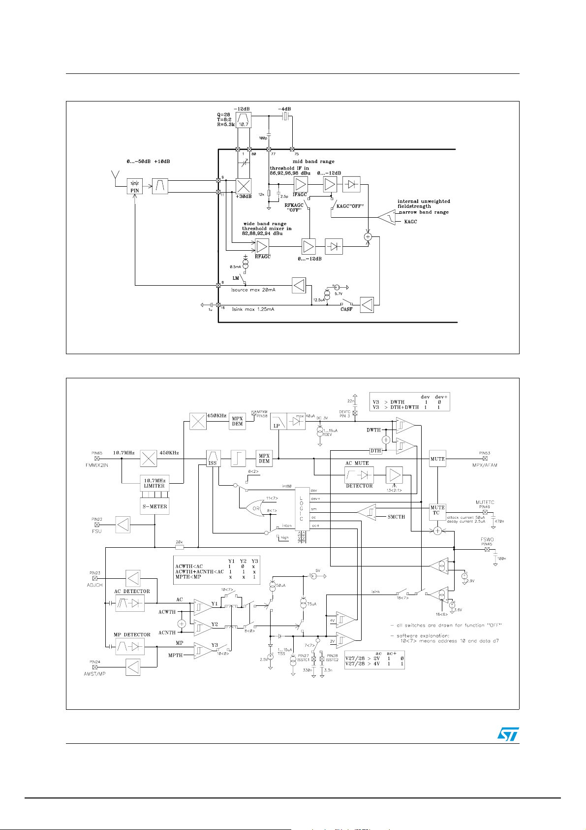
DOCUMENT CD00108485 REVISION 1.0 ACTIVE DATE 11-May-2006 page: 64/75
Appendix TDA7540B
Figure 10. Block diagram keying AGC
Figure 11. Block diagram ISS function
64/75
Copyright STMicroelectronics COMPANY INTERNAL Unauthorized reproduction and communication strictly prohibited

DOCUMENT CD00108485 REVISION 1.0 ACTIVE DATE 11-May-2006 page: 65/75
TDA7540B Appendix
Block Diagram Quality Detection Principle (without overdeviation correction)
Table 51.
Signal LOW HIGH
ac No adjacent channel Adjacent channel present
ac+ No strong adjacent channel Adjacent channel higher as ac
sm Fieldstrength higher as softmute threshold Fieldstrength lower as softmute threshold
dev Deviation lower as threshold DWTH Deviation higher as threshold DWTH
dev+ Deviation lower as threshold DTH*DWTH Deviation higher as threshold DTH*DWTH
inton ISS filter off by logic (wide) ISS filter on by logic
int80 ISS filter 120kHz (mid) ISS filter 80kHz (narrow)
Table 52.
Input Signals Mode1 Mode2
ac ac+ sm dev dev+ inton int80 Function inton int80 Function
000000 0wide0 0wide
000100 0wide0 0wide
000110 0wide0 0wide
0 0 1 0 0 1 1 narrow 1 1 narrow
001100 0wide1 0mid
001110 0wide0 0wide
100001 1narrow1 0mid
1 1 0 0 0 1 1 narrow 1 1 narrow
100101 0mid1 0mid
110111 0mid1 1narrow
1 0 1 0 0 1 1 narrow 1 1 narrow
1 1 1 0 0 1 1 narrow 1 1 narrow
101101 0mid1 0mid
111101 0mid1 1narrow
101111 0mid1 0mid
111111 0mid1 1narrow
65/75
Copyright STMicroelectronics COMPANY INTERNAL Unauthorized reproduction and communication strictly prohibited

DOCUMENT CD00108485 REVISION 1.0 ACTIVE DATE 11-May-2006 page: 66/75
Appendix TDA7540B
Figure 12. Block diagram AM part
66/75
Copyright STMicroelectronics COMPANY INTERNAL Unauthorized reproduction and communication strictly prohibited

DOCUMENT CD00108485 REVISION 1.0 ACTIVE DATE 11-May-2006 page: 67/75
TDA7540B Appendix
Figure 13. Blockdiagram AM IF Noise Blanker
Figure 14. Block diagram Stereodecoder
67/75
Copyright STMicroelectronics COMPANY INTERNAL Unauthorized reproduction and communication strictly prohibited

DOCUMENT CD00108485 REVISION 1.0 ACTIVE DATE 11-May-2006 page: 68/75
Appendix TDA7540B
Figure 15. Block diagram Audio Noise Blanker
Figure 16. Block diagram Multipath Detection
68/75
Copyright STMicroelectronics COMPANY INTERNAL Unauthorized reproduction and communication strictly prohibited
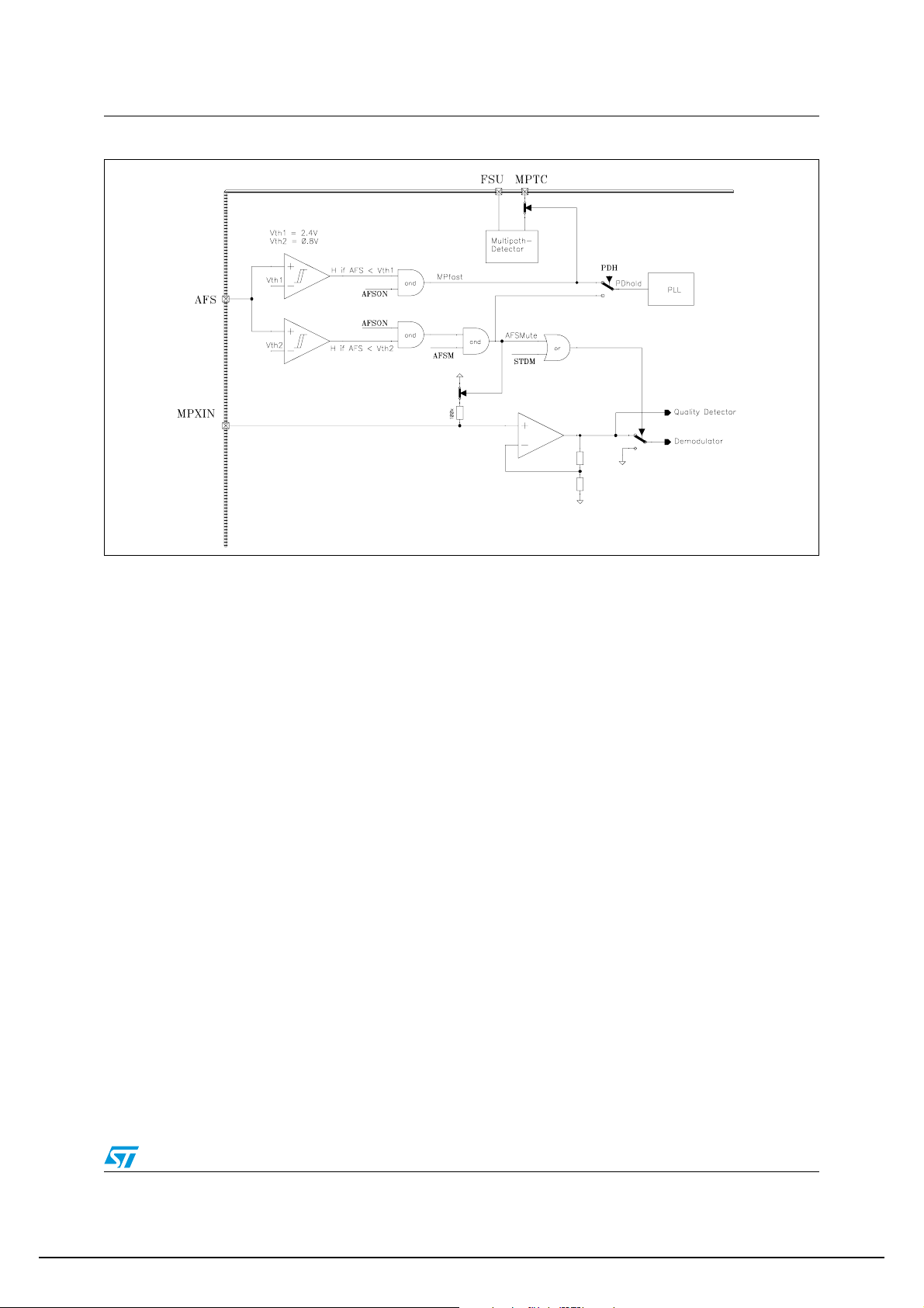
DOCUMENT CD00108485 REVISION 1.0 ACTIVE DATE 11-May-2006 page: 69/75
TDA7540B Appendix
Figure 17. Block diagram AFS function
69/75
Copyright STMicroelectronics COMPANY INTERNAL Unauthorized reproduction and communication strictly prohibited

DOCUMENT CD00108485 REVISION 1.0 ACTIVE DATE 11-May-2006 page: 70/75
Part List (Application and measurment circuit) TDA7540B
7 Part List (Application and measurment circuit)
Table 53. Part list
Item Description
F1 TOKO 5KG 611SNS-A096GO
F2 TOKO 5KM 396INS-A467AO
F3 TOKO MC152 E558CN-100021=P3
F4 TOKO 7PSG P826RC-5134N
F5 TOKO PGL 5PGLC-5103N
L1 TOKO FSLM 2520-150 15µH
L2,L4 TOKO FSLM 2520-680 68µH
L3,L8 SIEMENS SIMID03 B82432 1mH
L5 TOKO LL 2012-220
L6 TOKO LL 2012-270
L7 TOKO LL 2012-22.0
CF1,CF2 muRata SFE10.7MS3A10-A 180KHz or (TOKO CFSK107M3-AE-20X)
CF3 muRata SFE10.7MJA10-A 150KHz or (TOKO CFSK107M4-AE-20X)
CF4 muRata SFPS 450H 6KHz or (TOKO ARLFC450T)
D1 TOSHIBA 1SV172
D2,D3 TOKO KP2311E
D4 TOKO KV1370NT
D5 PHILIPS BB156
Q1 TOSHIBA HN3G01J
70/75
Copyright STMicroelectronics COMPANY INTERNAL Unauthorized reproduction and communication strictly prohibited

DOCUMENT CD00108485 REVISION 1.0 ACTIVE DATE 11-May-2006 page: 71/75
TDA7540B Application circuit
8 Application circuit
Figure 18. Application circuit
71/75
Copyright STMicroelectronics COMPANY INTERNAL Unauthorized reproduction and communication strictly prohibited

DOCUMENT CD00108485 REVISION 1.0 ACTIVE DATE 11-May-2006 page: 72/75
Application Notes TDA7540B
9 Application Notes
Following items are important to get highest performance of TDA7540 in application:
1. In order to avoid leakage current from PLL loop filter input to ground a guardring is
recommended around loop filter PIN’s with PLL reference (VREF2) voltage potential.
2. Distance between Xtal and VCO input PIN 18 should be far as possible and Xtal
package should get a shield versus ground.
3. Blocking of VCO supply should be near at PIN 20 and PIN 21.
4. Blocking of VCC2 supply should be near at PIN 64 and PIN 61.
5. Wire lenght to FM mixer1-input and -output should be symetrically and short.
6. FM demodulator capacitance at PIN 56 should be sense connected as short as
possible versus demodulator ground at PIN 57.
7. Wire lenght from AM mixer tank output to 9KHz ceramic filter input has to be short as
possible.
8. To minimize “AM TWEET” the AM demodulator capacitor should be connected versus
GNDVCC1 at PIN 41 and FSU output at PIN 22 should be filtered with capacitor of
about 2,2nF versus GNDVCC2.
72/75
Copyright STMicroelectronics COMPANY INTERNAL Unauthorized reproduction and communication strictly prohibited

DOCUMENT CD00108485 REVISION 1.0 ACTIVE DATE 11-May-2006 page: 73/75
TDA7540B Package Information
10 Package Information
In order to meet environmental requirements, ST offers these devices in ECOPACK®
packages. These packages have a Lead-free second level interconnect. The category of
second Level Interconnect is marked on the package and on the inner box label, in
compliance with JEDEC Standard JESD97.
The maximum ratings related to soldering conditions are also marked on the inner box label.
ECOPACK is an ST trademark. ECOPACK specifications are available at: www.st.com.
Figure 19. TQFP80 (14x14x1.40mm) Mechanical Data & Package Dimensions
DIM.
A 1.60 0.063
A1 0.05 0.15 0.002 0.006
A2 1.35 1.40 1.45 0.053 0.055 0.057
B 0.22 0.32 0.38 0.009 0.013 0.015
C 0.09 0.20 0.003 0.008
D 16.00 0.630
D1 14.00 0.551
D3 12.35 0.295
e 0.65 0.0256
E 16.00 0.630
E1 14.00 0.551
E3 12.35 0.486
L 0.45 0.60 0.75 0.018 0.024 0.030
L1 1.00 0.0393
K3.5
mm inch
MIN. TYP. MAX. MIN. TYP. MAX.
°
(min.), 7°(max.)
D
D1
D3
60
61
OUTLINE AND
MECHANICAL DATA
TQFP80
(14x14x1.40mm)
A
A2
41
40
0.10mm
Seating Plane
A1
.004
e
E3
E1 E
B
IDENTIFICATION
80
1
PIN 1
21
20
TQFP80L
Gage plane
0.25mm
K
L
L1
C
73/75
Copyright STMicroelectronics COMPANY INTERNAL Unauthorized reproduction and communication strictly prohibited

DOCUMENT CD00108485 REVISION 1.0 ACTIVE DATE 11-May-2006 page: 74/75
Revision history TDA7540B
11 Revision history
Table 54. Document revision history
Date Revision Changes
10-May-2006 1 Initial release.
74/75
Copyright STMicroelectronics COMPANY INTERNAL Unauthorized reproduction and communication strictly prohibited

DOCUMENT CD00108485 REVISION 1.0 ACTIVE DATE 11-May-2006 page: 75/75
TDA7540B
Please Read Carefully:
Information in this document is provided solely in connection with ST products. STMicroelectronics NV and its subsidiaries (“ST”) reserve the
right to make changes, corrections, modifications or improvements, to this document, and the products and services described herein at any
time, without notice.
All ST products are sold pursuant to ST’s terms and conditions of sale.
Purchasers are solely responsible for the choice, selection and use of the ST products and services described herein, and ST assumes no
liability whatsoever relating to the choice, selection or use of the ST products and services described herein.
No license, express or implied, by estoppel or otherwise, to any intellectual property rights is granted under this document. If any part of this
document refers to any third party products or services it shall not be deemed a license grant by ST for the use of such third party products
or services, or any intellectual property contained therein or considered as a warranty covering the use in any manner whatsoever of such
third party products or services or any intellectual property contained therein.
UNLESS OTHERWISE SET FORTH IN ST’S TERMS AND CONDITIONS OF SALE ST DISCLAIMS ANY EXPRESS OR IMPLIED
WARRANTY WITH RESPECT TO THE USE AND/OR SALE OF ST PRODUCTS INCLUDING WITHOUT LIMITATION IMPLIED
WARRANTIES OF MERCHANTABILITY, FITNESS FOR A PARTICULAR PURPOSE (AND THEIR EQUIVALENTS UNDER THE LAWS
OF ANY JURISDICTION), OR INFRINGEMENT OF ANY PATENT, COPYRIGHT OR OTHER INTELLECTUAL PROPERTY RIGHT.
UNLESS EXPRESSLY APPROVED IN WRITING BY AN AUTHORIZE REPRESENTATIVE OF ST, ST PRODUCTS ARE NOT DESIGNED,
AUTHORIZED OR WARRANTED FOR USE IN MILITARY, AIR CRAFT, SPACE, LIFE SAVING, OR LIFE SUSTAINING APPLICATIONS,
NOR IN PRODUCTS OR SYSTEMS, WHERE FAILURE OR MALFUNCTION MAY RESULT IN PERSONAL INJURY, DEATH, OR
SEVERE PROPERTY OR ENVIRONMENTAL DAMAGE.
Resale of ST products with provisions different from the statements and/or technical features set forth in this document shall immediately void
any warranty granted by ST for the ST product or service described herein and shall not create or extend in any manner whatsoever, any
liability of ST.
ST and the ST logo are trademarks or registered trademarks of ST in various countries.
Information in this document supersedes and replaces all information previously supplied.
The ST logo is a registered trademark of STMicroelectronics. All other names are the property of their respective owners.
© 2006 STMicroelectronics - All rights reserved
STMicroelectronics group of companies
Australia - Belgium - Brazil - Canada - China - Czech Republic - Finland - France - Germany - Hong Kong - India - Israel - Italy - Japan -
Malaysia - Malta - Morocco - Singapore - Spain - Sweden - Switzerland - United Kingdom - United States of America
www.st.com
75/75
Copyright STMicroelectronics COMPANY INTERNAL Unauthorized reproduction and communication strictly prohibited
 Loading...