

Page 1
FM car-radio tuner IC with intelligent selectivity system (ISS)
Features
FM part
■ RF AGC generation by RF and IF detection
■ I/Q mixer for 1
rejection
■ 2 programmable IF-gain stages
■ Mixer for 2
■ Internal 450 kHz bandpass filter with three
bandwidths controlled by ISS
■ Fully integrated FM-demodulator with noise
cancellation
Additional features
■ VCO for world tuning range
■ High performance fast PLL for RDS-system
■ IF counter with search stop signal
■ Quality detector for level, deviation, adjacent
channel and multipath
■ Quality detection informations as analog
signals external available
■ ISS (intelligent selectivity system) for
cancellation of adjacent channel and noise
influences
Table 1. Device summary
st
FM IF 10.7 MHz with image
nd
IF 450 kHz
TDA7512F
LQFP64
■ Adjacent channel mute
■ Fully electronic alignment
■ All functions I
Description
The TDA7512F is a high performance tuner circuit
for FM car-radio. It contains mixer, IF amplifier,
demodulator, quality detection, ISS filter and PLL
synthesizer with IF counter on a single chip. Use
of BiCMOS technology allows the implementation
of several tuning functions and a minimum of
external components.
2
C bus controlled
Order code Package Packing
E-TDA7512F LQFP64 Tray
E-TDA7512FTR LQFP64 Tape and reel
June 2009 Doc ID 12668 Rev 2 1/45
www.st.com
1
Page 2

Contents TDA7512F
Contents
1 Block diagram . . . . . . . . . . . . . . . . . . . . . . . . . . . . . . . . . . . . . . . . . . . . . . 6
2 Pin description . . . . . . . . . . . . . . . . . . . . . . . . . . . . . . . . . . . . . . . . . . . . . 7
3 Electrical specifications . . . . . . . . . . . . . . . . . . . . . . . . . . . . . . . . . . . . . 10
3.1 Thermal data . . . . . . . . . . . . . . . . . . . . . . . . . . . . . . . . . . . . . . . . . . . . . . 10
3.2 Absolute maximum ratings . . . . . . . . . . . . . . . . . . . . . . . . . . . . . . . . . . . . 10
3.3 Electrical characteristics . . . . . . . . . . . . . . . . . . . . . . . . . . . . . . . . . . . . . . 10
4 Functional description . . . . . . . . . . . . . . . . . . . . . . . . . . . . . . . . . . . . . . 17
4.1 Mixer 1, AGC and 1.IF . . . . . . . . . . . . . . . . . . . . . . . . . . . . . . . . . . . . . . . 17
4.2 Mixer 2, limiter and demodulator . . . . . . . . . . . . . . . . . . . . . . . . . . . . . . . 17
4.3 Quality detection and ISS . . . . . . . . . . . . . . . . . . . . . . . . . . . . . . . . . . . . . 17
4.3.1 Fieldstrength . . . . . . . . . . . . . . . . . . . . . . . . . . . . . . . . . . . . . . . . . . . . . 17
4.3.2 Adjacent channel detector . . . . . . . . . . . . . . . . . . . . . . . . . . . . . . . . . . . 17
4.3.3 Multipath detector . . . . . . . . . . . . . . . . . . . . . . . . . . . . . . . . . . . . . . . . . 18
4.3.4 450 kHz IF narrow bandpass filter (ISS filter) . . . . . . . . . . . . . . . . . . . . 18
4.3.5 Deviation detector . . . . . . . . . . . . . . . . . . . . . . . . . . . . . . . . . . . . . . . . . 18
4.3.6 ISS switch logic . . . . . . . . . . . . . . . . . . . . . . . . . . . . . . . . . . . . . . . . . . . 18
4.4 Soft Mute control . . . . . . . . . . . . . . . . . . . . . . . . . . . . . . . . . . . . . . . . . . . 18
4.5 PLL and IF counter section . . . . . . . . . . . . . . . . . . . . . . . . . . . . . . . . . . . 19
4.5.1 PLL frequency synthesizer block . . . . . . . . . . . . . . . . . . . . . . . . . . . . . . 19
4.5.2 Frequency generation for phase comparison . . . . . . . . . . . . . . . . . . . . 19
4.5.3 Three state phase comparator . . . . . . . . . . . . . . . . . . . . . . . . . . . . . . . . 19
4.5.4 Charge pump current generator . . . . . . . . . . . . . . . . . . . . . . . . . . . . . . 19
4.5.5 Inlock detector . . . . . . . . . . . . . . . . . . . . . . . . . . . . . . . . . . . . . . . . . . . . 20
4.5.6 Low noise CMOS op-amp . . . . . . . . . . . . . . . . . . . . . . . . . . . . . . . . . . . 20
4.5.7 IF counter block . . . . . . . . . . . . . . . . . . . . . . . . . . . . . . . . . . . . . . . . . . . 20
4.5.8 Sampling timer . . . . . . . . . . . . . . . . . . . . . . . . . . . . . . . . . . . . . . . . . . . . 20
4.5.9 Intermediate frequency main counter . . . . . . . . . . . . . . . . . . . . . . . . . . 20
4.5.10 Adjustment of the measurement sequence time . . . . . . . . . . . . . . . . . . 21
4.5.11 Adjust of the frequency value . . . . . . . . . . . . . . . . . . . . . . . . . . . . . . . . . 21
4.6 I2C bus interface . . . . . . . . . . . . . . . . . . . . . . . . . . . . . . . . . . . . . . . . . . . . 21
4.6.1 Data transition . . . . . . . . . . . . . . . . . . . . . . . . . . . . . . . . . . . . . . . . . . . . 21
2/45 Doc ID 12668 Rev 2
Page 3

TDA7512F Contents
4.6.2 Start condition . . . . . . . . . . . . . . . . . . . . . . . . . . . . . . . . . . . . . . . . . . . . 21
4.6.3 Stop condition . . . . . . . . . . . . . . . . . . . . . . . . . . . . . . . . . . . . . . . . . . . . 21
4.6.4 Acknowledge . . . . . . . . . . . . . . . . . . . . . . . . . . . . . . . . . . . . . . . . . . . . . 21
4.6.5 Data transfer . . . . . . . . . . . . . . . . . . . . . . . . . . . . . . . . . . . . . . . . . . . . . 22
4.6.6 Device addressing . . . . . . . . . . . . . . . . . . . . . . . . . . . . . . . . . . . . . . . . . 22
4.6.7 Write operation . . . . . . . . . . . . . . . . . . . . . . . . . . . . . . . . . . . . . . . . . . . 22
4.6.8 Read operation . . . . . . . . . . . . . . . . . . . . . . . . . . . . . . . . . . . . . . . . . . . 22
5 Software specification . . . . . . . . . . . . . . . . . . . . . . . . . . . . . . . . . . . . . . 24
5.1 Address organization . . . . . . . . . . . . . . . . . . . . . . . . . . . . . . . . . . . . . . . . 24
5.2 Control register function . . . . . . . . . . . . . . . . . . . . . . . . . . . . . . . . . . . . . . 25
5.3 Data byte specification . . . . . . . . . . . . . . . . . . . . . . . . . . . . . . . . . . . . . . . 27
6 Package information . . . . . . . . . . . . . . . . . . . . . . . . . . . . . . . . . . . . . . . . 38
Appendix A Block diagrams . . . . . . . . . . . . . . . . . . . . . . . . . . . . . . . . . . . . . . . . . 39
Appendix B Application notes. . . . . . . . . . . . . . . . . . . . . . . . . . . . . . . . . . . . . . . . 43
7 Revision history . . . . . . . . . . . . . . . . . . . . . . . . . . . . . . . . . . . . . . . . . . . 44
Doc ID 12668 Rev 2 3/45
Page 4

List of tables TDA7512F
List of tables
Table 2. Pin description . . . . . . . . . . . . . . . . . . . . . . . . . . . . . . . . . . . . . . . . . . . . . . . . . . . . . . . . . . . 7
Table 3. Thermal data. . . . . . . . . . . . . . . . . . . . . . . . . . . . . . . . . . . . . . . . . . . . . . . . . . . . . . . . . . . . 10
Table 4. Absolute maximum ratings . . . . . . . . . . . . . . . . . . . . . . . . . . . . . . . . . . . . . . . . . . . . . . . . . 10
Table 5. Electrical characteristics . . . . . . . . . . . . . . . . . . . . . . . . . . . . . . . . . . . . . . . . . . . . . . . . . . . 10
Table 6. Address organization . . . . . . . . . . . . . . . . . . . . . . . . . . . . . . . . . . . . . . . . . . . . . . . . . . . . . 24
Table 7. Control register function . . . . . . . . . . . . . . . . . . . . . . . . . . . . . . . . . . . . . . . . . . . . . . . . . . . 25
Table 8. Subaddress. . . . . . . . . . . . . . . . . . . . . . . . . . . . . . . . . . . . . . . . . . . . . . . . . . . . . . . . . . . . . 27
Table 9. Addr 0 charge pump control . . . . . . . . . . . . . . . . . . . . . . . . . . . . . . . . . . . . . . . . . . . . . . . . 27
Table 10. Addr 1 PLL counter 1 (LSB) . . . . . . . . . . . . . . . . . . . . . . . . . . . . . . . . . . . . . . . . . . . . . . . . 28
Table 11. Addr 2 PLL counter 2 (MSB). . . . . . . . . . . . . . . . . . . . . . . . . . . . . . . . . . . . . . . . . . . . . . . . 28
Table 12. Addr 3,4 TV1,2 (offset refered to tuning voltage PIN 28) . . . . . . . . . . . . . . . . . . . . . . . . . . 29
Table 13. Addr 5 IF counter control 1 . . . . . . . . . . . . . . . . . . . . . . . . . . . . . . . . . . . . . . . . . . . . . . . . . 29
Table 14. Addr 6 IF Counter Control 2 . . . . . . . . . . . . . . . . . . . . . . . . . . . . . . . . . . . . . . . . . . . . . . . . 29
Table 15. Addr 7 not valid. . . . . . . . . . . . . . . . . . . . . . . . . . . . . . . . . . . . . . . . . . . . . . . . . . . . . . . . . . 30
Table 16. Addr 8 quality ISS filter . . . . . . . . . . . . . . . . . . . . . . . . . . . . . . . . . . . . . . . . . . . . . . . . . . . . 30
Table 17. Addr 9 quality detection adjacent channel . . . . . . . . . . . . . . . . . . . . . . . . . . . . . . . . . . . . . 31
Table 18. Addr 10 quality detection multipath. . . . . . . . . . . . . . . . . . . . . . . . . . . . . . . . . . . . . . . . . . . 31
Table 19. Addr 11 quality deviation detection . . . . . . . . . . . . . . . . . . . . . . . . . . . . . . . . . . . . . . . . . . . 32
Table 20. Addr 12 soft mute control 1. . . . . . . . . . . . . . . . . . . . . . . . . . . . . . . . . . . . . . . . . . . . . . . . . 32
Table 21. Addr 13 soft mute control 2. . . . . . . . . . . . . . . . . . . . . . . . . . . . . . . . . . . . . . . . . . . . . . . . . 33
Table 22. Addr 14 VCODIV/PLLREF . . . . . . . . . . . . . . . . . . . . . . . . . . . . . . . . . . . . . . . . . . . . . . . . . 33
Table 23. Addr 15 FM AGC . . . . . . . . . . . . . . . . . . . . . . . . . . . . . . . . . . . . . . . . . . . . . . . . . . . . . . . . 34
Table 24. Addr 16 not valid. . . . . . . . . . . . . . . . . . . . . . . . . . . . . . . . . . . . . . . . . . . . . . . . . . . . . . . . . 35
Table 25. Addr 17 FM demodulator fine adjust. . . . . . . . . . . . . . . . . . . . . . . . . . . . . . . . . . . . . . . . . . 35
Table 26. Addr 18 s-meter slider . . . . . . . . . . . . . . . . . . . . . . . . . . . . . . . . . . . . . . . . . . . . . . . . . . . . 35
Table 27. Addr 19 IF GAIN/XTAL adjust. . . . . . . . . . . . . . . . . . . . . . . . . . . . . . . . . . . . . . . . . . . . . . . 36
Table 28. Addr 20 tank adjust . . . . . . . . . . . . . . . . . . . . . . . . . . . . . . . . . . . . . . . . . . . . . . . . . . . . . . . 36
Table 29. Addr 21 I/Q mixer 1 adjust . . . . . . . . . . . . . . . . . . . . . . . . . . . . . . . . . . . . . . . . . . . . . . . . . 37
Table 30. Addr 22 test control 1 . . . . . . . . . . . . . . . . . . . . . . . . . . . . . . . . . . . . . . . . . . . . . . . . . . . . . 37
Table 31. Addr 23 test control 2 . . . . . . . . . . . . . . . . . . . . . . . . . . . . . . . . . . . . . . . . . . . . . . . . . . . . . 37
Table 32. Addr 24 Test control 3 . . . . . . . . . . . . . . . . . . . . . . . . . . . . . . . . . . . . . . . . . . . . . . . . . . . . 37
Table 33. Addr 25 test control 4 . . . . . . . . . . . . . . . . . . . . . . . . . . . . . . . . . . . . . . . . . . . . . . . . . . . . . 37
Table 34. Block diagram quality detection principle (without overdeviation correction) . . . . . . . . . . . 41
Table 35. Input signals modes . . . . . . . . . . . . . . . . . . . . . . . . . . . . . . . . . . . . . . . . . . . . . . . . . . . . . . 41
Table 36. Part list (application- and measurment circuit) . . . . . . . . . . . . . . . . . . . . . . . . . . . . . . . . . . 42
Table 37. Document revision history . . . . . . . . . . . . . . . . . . . . . . . . . . . . . . . . . . . . . . . . . . . . . . . . . 44
4/45 Doc ID 12668 Rev 2
Page 5

TDA7512F List of figures
List of figures
Figure 1. Block Diagram . . . . . . . . . . . . . . . . . . . . . . . . . . . . . . . . . . . . . . . . . . . . . . . . . . . . . . . . . . . 6
Figure 2. Pin connection (top view) . . . . . . . . . . . . . . . . . . . . . . . . . . . . . . . . . . . . . . . . . . . . . . . . . . . 7
Figure 3. Interface protocol . . . . . . . . . . . . . . . . . . . . . . . . . . . . . . . . . . . . . . . . . . . . . . . . . . . . . . . . 24
Figure 4. LQFP64 mechanical data and package dimensions . . . . . . . . . . . . . . . . . . . . . . . . . . . . . 38
Figure 5. Block diagram I/Q mixer . . . . . . . . . . . . . . . . . . . . . . . . . . . . . . . . . . . . . . . . . . . . . . . . . . . 39
Figure 6. Block diagram VCO . . . . . . . . . . . . . . . . . . . . . . . . . . . . . . . . . . . . . . . . . . . . . . . . . . . . . . 39
Figure 7. Block diagram keying AGC . . . . . . . . . . . . . . . . . . . . . . . . . . . . . . . . . . . . . . . . . . . . . . . . . 40
Figure 8. Block diagram ISS function. . . . . . . . . . . . . . . . . . . . . . . . . . . . . . . . . . . . . . . . . . . . . . . . . 40
Figure 9. Application circuit . . . . . . . . . . . . . . . . . . . . . . . . . . . . . . . . . . . . . . . . . . . . . . . . . . . . . . . . 42
Doc ID 12668 Rev 2 5/45
Page 6
Block diagram TDA7512F
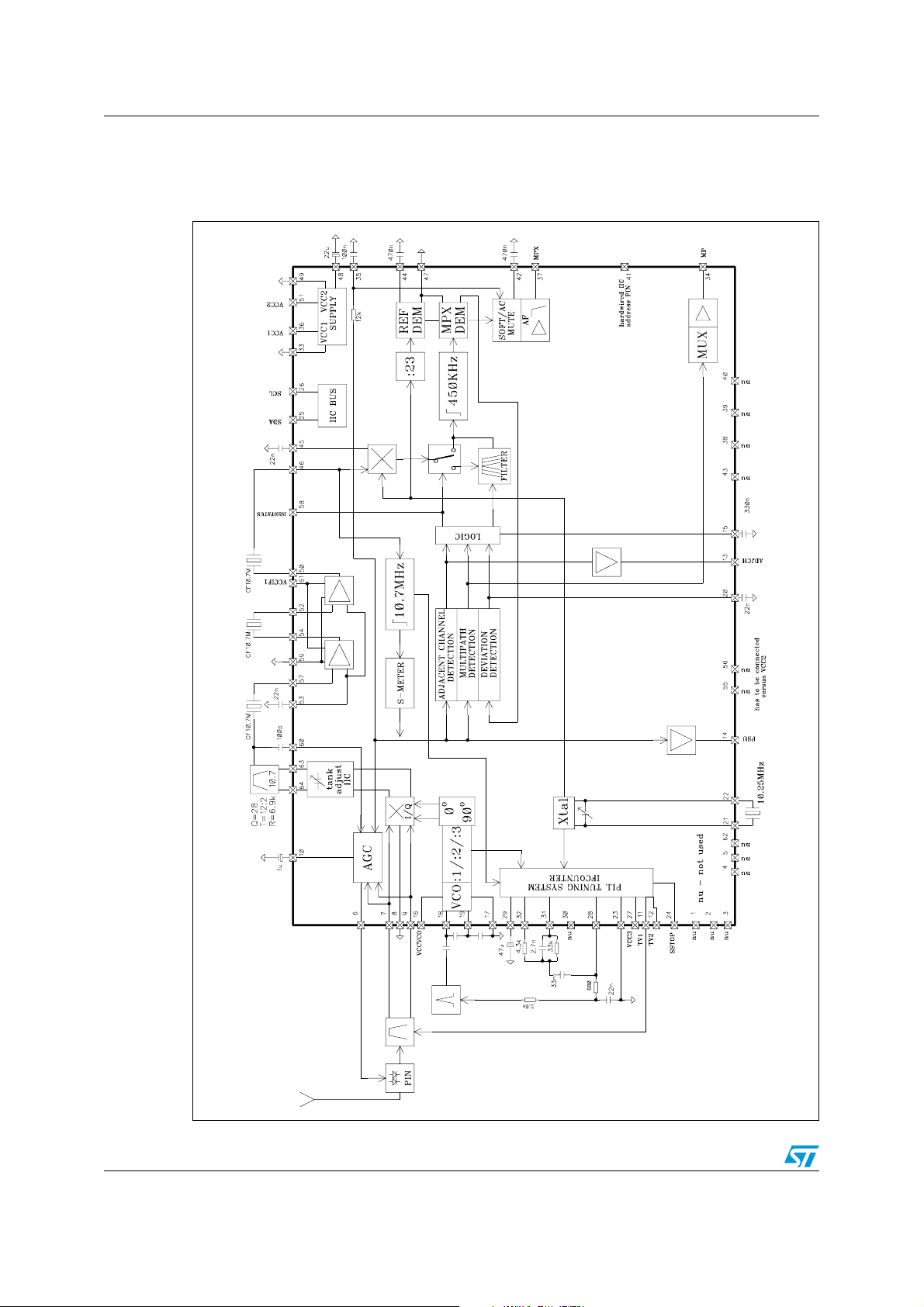
1 Block diagram
Figure 1. Block Diagram
6/45 Doc ID 12668 Rev 2
Page 7
TDA7512F Pin description
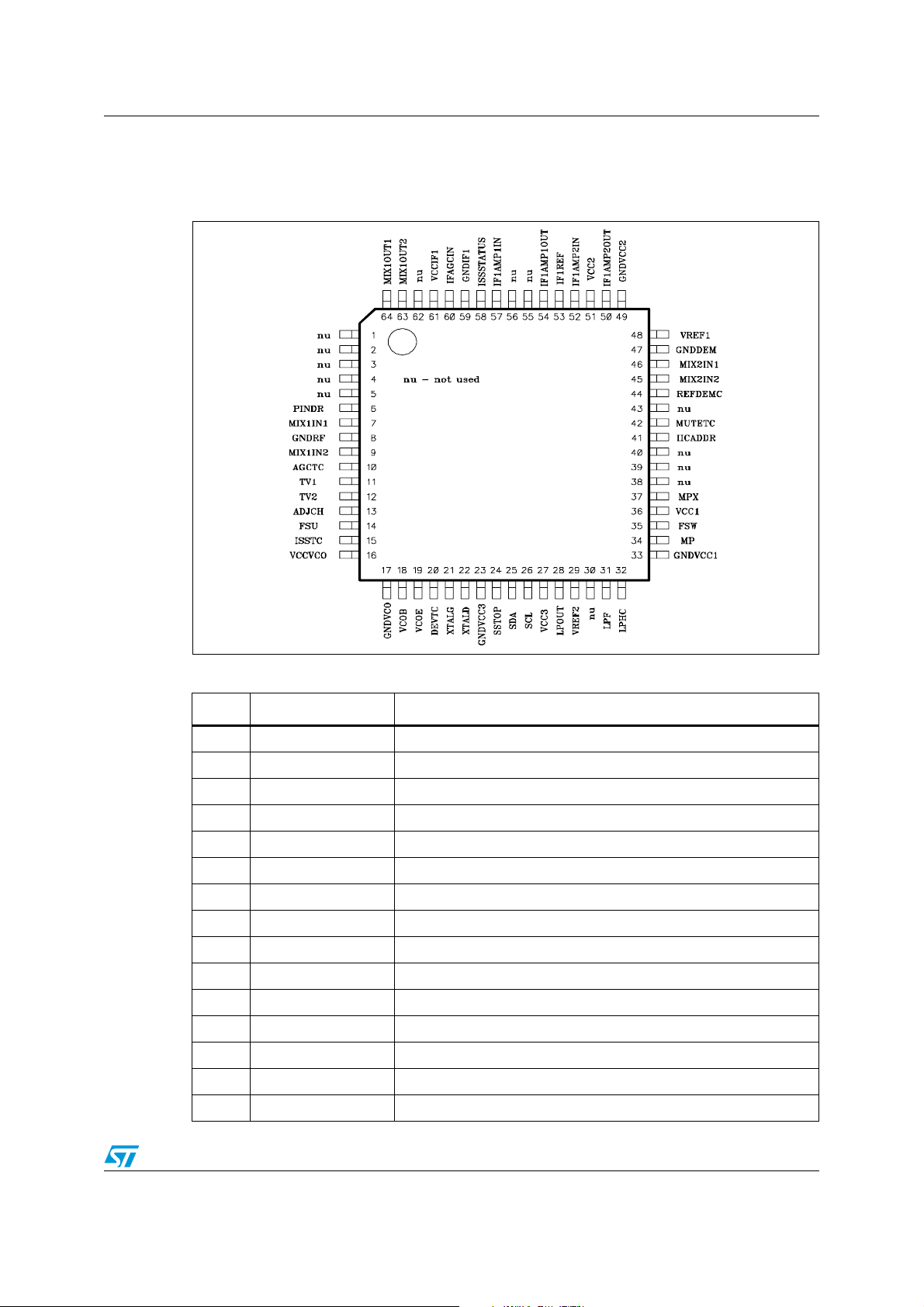
2 Pin description
Figure 2. Pin connection (top view)
Table 2. Pin description
Pin # Pin name Function
1 nu not used - to be left open
2 nu not used - to be left open
3 nu not used - to be left open
4 nu not used - to be left open
5 nu not used - to be left open
6 PINDR PIN Diode Driver Output
7 MIX1IN1 Input1 Mixer1
8 GNDRF RF Ground
9 MIX1IN2 Input2 Mixer1
10 AGCTC AGC Time Constant
11 TV1 Tuning Voltage Preselection1
12 TV2 Tuning Voltage Preselection2
13 ADJCH Ident. Adjacent Channel Output
14 FSU Unweighted Fieldstrength Output
15 ISSTC Time Constant for ISS Filter Switch
Doc ID 12668 Rev 2 7/45
Page 8
Pin description TDA7512F
Table 2. Pin description (continued)
Pin # Pin name Function
16 VCCVCO VCO Supply
17 GNDVCO VCO Ground
18 VCOB VCO Input Base
19 VCOE VCO Output Emitter
20 DEVTC Deviation Detector Time Constant
21 XTALG Xtal Oscillator to MOS Gate
22 XTALD Xtal Oscillator to MOS Drain
23 GNDVCC3 VCC3 Ground
24 SSTOP Search Stop Output
2
25 SDA I
26 SCL I
27 VCC3 Supply Tuning Voltage
28 LPOUT Op Amp Output to PLL Loop Filters
29 VREF2 Voltage Reference for PLL Op Amp
30 nu not used - to be left open
C-Bus Data
2
C-Bus Clock
31 LPF Op Amp Input to PLL Loop Filter
32 LPHC High Current PLL Loop Filter Input
33 GNDVCC1 Digital Ground
34 MP Ident. Multipath Output
35 FSW Weighted Fieldstrength Output
36 VCC1 Digital Supply
37 MPX MPX Output
38 nu not used - to be left open
39 nu not used - to be left open
40 nu not used - to be left open
41 IICADDR Hardwired IIC-Address PIN
42 MUTETC Softmute Time Constant
43 nu not used - to be left open
44 REFDEMC Demodulator Reference
45 MIX2IN2 MIX2 Input1
46 MIX2IN1 MIX2 Input2
47 GNDDEM Ground Demodulator
48 VREF1 Reference 5V
49 GNDVCC2 Analog Ground
50 IF1AMP2OUT IF1 Amplifier2 Output
8/45 Doc ID 12668 Rev 2
Page 9

TDA7512F Pin description
Table 2. Pin description (continued)
Pin # Pin name Function
51 VCC2 Analog Supply
52 IF1AMP2IN IF1 Amplifier2 Input
53 IF1REF IF1 Amplifier Reference
54 IF1AMP1OUT IF1 Amplifier1 Output
55 nc not used - has to be connected versus VCC2
56 nc not used - has to be connected versus VCC2
57 IF1AMP1IN IF1 Amplifier1 Input
58 ISSSTATUS ISS Filter Status
59 GNDIF1 IF1 Ground
60 IFAGCIN IF AGC Input
61 VCCIF1 IF1 Supply
62 nu not used - to be left open
63 MIX1OUT2 MIX Tank 10.7MHz
64 MIX1OUT1 MIX Tank 10.7MHz
Doc ID 12668 Rev 2 9/45
Page 10
Electrical specifications TDA7512F
3 Electrical specifications
3.1 Thermal data
Table 3. Thermal data
Symbol Parameter Value Unit
R
th(j-amb)
Thermal resistance junction-to-ambient 68 max. °C/W
3.2 Absolute maximum ratings
Table 4. Absolute maximum ratings
Symbol Parameter Value Unit
V
T
amb
T
Supply voltage 10.5 V
S
Ambient temperature -40 to 85 °C
Storage temperature -55 to +150 °C
stg
3.3 Electrical characteristics
T
= +25 °C, V
amb
dev. = 40 kHz, f
circuit, unless otherwise specified.
Table 5. Electrical characteristics
Symbol Parameter Test conditions Min. Typ. Max. Unit
Supply
CC1
= 1 kHz, f
MOD
= V
CC2
= V
= V
CC3
= 10.7 MHz, f
IF1
CCVCO
= V
CCMIX1
= 450 kHz, f
IF2
= V
= 8.5 V, fRF = 98 MHz,
CCIF1
= 10.25 MHz, in application
Xtal
V
CC1
V
CC2
V
CC3
V
CCVCO
V
CCMIX1
V
CCIF1
I
CC1
I
CC2
I
CC3
I
CCVCO
I
CCMIX1
I
CCIF1
Digital supply voltage - 7.5 8.5 10 V
Analog supply voltage - 7.5 8.5 10 V
Analog tuning voltage - 7.5 8.5 10 V
VCO supply voltage - 7.5 8.5 10 V
MIX1 supply voltage - 7.5 8.5 10 V
IF1 supply voltage - 7.5 8.5 10 V
Supply current - - 7.5 - mA
Supply current VCO:3 - 70 - mA
Supply current - - 2 - mA
Supply current - - 9 - mA
Supply current - - 8 - mA
Supply current - - 6 - mA
10/45 Doc ID 12668 Rev 2
Page 11
TDA7512F Electrical specifications
Table 5. Electrical characteristics (continued)
Symbol Parameter Test conditions Min. Typ. Max. Unit
Reference voltages
V
V
REF1
REF2
Internal reference voltage I
Internal reference voltage I
Wide band RF AGC
V
7-9
V
7-9
Lower threshold start V10 = 2.5 V - 85 - dBµV
Upper threshold start V10 = 2.5 V - 96 - dBµV
Narrow band IF & keying AGC
V
60
V
60
V
60
V
35
Lower threshold start KAGC = off, V
Upper threshold start KAGC = off, V
Lower threshold start with
KAGC
Start point KAGC
D Control range KAGC
R
IN
C
IN
Input resistance - - 10 - kΩ
Input capacitance - - 2.5 - pF
AGC time constant output
V
10
V
10
I
10
I
10
Max. AGC output voltage V
Min. AGC output voltage V
Min. AGC charge current V
Max. AGC discharge
current
= 0 mA - 5 - V
REF1
= 0 mA - 2.5 - V
REF2
= 0 mV
7-9
= 0 mV
7-9
KAGC = max, V
Δf
= 300 kHz
IF
KAGC = max, V
Δf
= 300 kHz
IF
generate FSW level at V
f
IF1
ΔV
= +0.4 V - 16 - dB
35
= 0 mV
7-9
= 50 mV
7-9
= 0 mV
7-9
= 50 mV
V
7-9
7-9
7-9
RMS
RMS
,; V10 = 2.5 V - -12.5 - µA
RMS
,; V10 = 2.5 V - 1.25 - mA
RMS
= 0 mV
= 0 mV
RMS
RMS
RMS,
RMS,
35
- 86 - dBµV
- 98 - dBµV
- 98 - dBµV
-3.6- V
V
-
REF1
+V
-0.5V
BE
V
AGC pin diode driver output
I
6
I
6
AGC OUT, current min. V
AGC OUT, current max. V
= 0 mV
7-9
= 50 mV
7-9
, V6 = 2.5 V - 50 - µA
RMS
, V6 = 2.5 V - -20 - mA
RMS
I/Q mixer 1 (10.7MHz)
R
R
C
V
g
IN
IN
OUT
7,9
m
Input resistance differential - 10 - kΩ
Input capacitance differential - 4 - pF
Output resistance differential 100 - kΩ
Input dc bias - - 3.2 - V
Conversion
transconductance
--17-mS
F Noise figure 400 Ω generator resistance - 3 - dB
Doc ID 12668 Rev 2 11/45
Page 12
Electrical specifications TDA7512F
Table 5. Electrical characteristics (continued)
Symbol Parameter Test conditions Min. Typ. Max. Unit
CP
1dB
IIP3 3
1dB compression point referred to diff. mixer input - 100 - dBµV
rd
order intermodulation - - 122 - dBµV
IQG I/Q gain adjust G -1 - +1 %
IQP I/Q phase adjust PH -7 - +8 DEG
IRR Image rejection ratio ratio wanted/image 30 40 - dB
IRR Image rejection ratio with gain and phase adjust 40 46 - dB
IF1 Amplifier1,2 (10.7 MHz)
G1
min
G1
max
G2
min
G2
max
R
IN
R
OUT
CP
1dB
IIP3 3rd order Intermodulation referred to 330 Ω
Min. gain IFG, referred to 330 Ω -9-dB
Max. gain IFG, referred to 330 Ω -15-dB
Min. gain IFG, referred to 330 Ω -9-dB
Max. gain IFG, referred to 330 Ω -11-dB
Input resistance - - 330 - Ω
Output resistance - - 330 - Ω
1dB compression point referred to 330 Ω input - 105 - dBµV
input - 126 - dBµV
Mixer 2 (450 kHz)
R
IN
V
46
V
48
Input impedance - - 330 - W
Max. input voltage - - 900 - mV
Limiting sensitivity S/N = 20dB - 25 - µV
G Mixer gain - - 18 - dB
RMS
Limiter 1 (450 kHz)
G
Limiter
Gain - - 80 - dB
Demodulator, audio output
THD Total harmonic distortion Dev.= 75 kHz, V
MPX output signal Dev.= 75 kHz - 500 - mV
Output resistance - - 50 - Ω
DC offset fine adjust DEM, MENA = 1 - 8.5 - mV
min
DC offset fine adjust DEM, MENA = 1 - 264 - mV
|
|
V
R
ΔV|
ΔV|
MPX
OUT
max
S/N Signal to noise Dev.= 40 kHz,V
= 10 mV
46
= 10 mV
46
Quality detection
S-meter, unweighted fieldstrength
V
46
V
14
Min. input voltage MIX2 - - 10 - µV
Fieldstrength output V46 = 0 V
RMS
12/45 Doc ID 12668 Rev 2
RMS
RMS
--0.1%
RMS
-76-dB
-0.1- V
Page 13

TDA7512F Electrical specifications
Table 5. Electrical characteristics (continued)
Symbol Parameter Test conditions Min. Typ. Max. Unit
R
V
ΔV
ΔV
ΔV
14
OUT
Fieldstrength output V46 = 1 V
voltage per decade SMSL = 0 - 1 - V
14
voltage per decade SMSL = 1 - 1.5 - V
14
S-meter offset SL, SMSL=1 -15 15 dB
14
RMS
-4.9- V
Output resistance - - 200 - W
TK Temp coeff. - - 0 - ppm/K
S-meter, weighted fieldstrength
R
V
V
OUT
35
35
Fieldstrength output V46 = 0 V
Fieldstrength output V46 = 1 V
RMS
RMS
Output resistance - - 12 - kΩ
-2.5- V
-4.9- V
Adjacent channel gain
G
min
G
max
Gain minimum ACG=0 - 32 - dB
Gain maximum ACG=1 - 38 - dB
Adjacent channel filter
f
HP
f
BP
f
-20dB
-3dB frequency highpass ACF=0 - 100 - kHz
Centre frequency ACF=1 - 100 - kHz
Attenuation 20dB - - 70 - kHz
Adjacent channel output
R
V
V
OUT
13
13
Output voltage low - - 0.1 - V
Output voltage high - - 4.9 - V
Output resistance - - 4 - kΩ
Multipath channel gain
G
min
G
max
Gain minimum MPG=0 - 12 - dB
Gain maximum MPG=1 - 23 - dB
Multipath bandpass filter
f
Lower
f
Upper
Centre frequency low MPF=0 - 19 - kHz
Centre frequency up MPF=1 - 31 - kHz
Q Quality factor - 5 10 -
Multipath output
R
V
V
OUT
34
34
Output voltage low - - 0.1 - V
Output voltage high - - 4.9 - V
Output resistance - - 2.5 - kΩ
Doc ID 12668 Rev 2 13/45
Page 14
Electrical specifications TDA7512F
Table 5. Electrical characteristics (continued)
Symbol Parameter Test conditions Min. Typ. Max. Unit
ISS (intelligent selectivity system)
Filter 450 kHz
f
centre
Centre frequency f
REF_intern
= 450 kHz - 450 - kHz
BW 3dB Bandwidth, -3dB ISS80 = 1 - 80 - kHz
BW 20dB Bandwidth, -20dB ISS80 = 1 - 150 - kHz
BW 3dB Bandwidth, -3dB ISS80 = 0 - 120 - kHz
BW 20dB Bandwidth, -20dB ISS80 = 0 - 250 - kHz
BW 3dB Bandwidth weather band ISS30 = 1 - 30 - kHz
BW 20dB -20dB weather band ISS30 = 1 - 80 - kHz
Adjacent channel ISS filter threshold
V
V
V
V
NTH
NTH
WTH
WTH
Internal low threshold ACNTH - 0 - V
Internal high threshold ACNTH - 0.3 - V
Internal low threshold ACWTH - 0.25 - V
Internal high threshold ACWTH - 0.95 - V
Multipath threshold
V
THMP
V
THMP
Internal low threshold MPTH - 0.50 - V
Internal high threshold MPTH - 1.25 - V
ISS filter time constant
I
15
I
15
I
15
I
15
I
15
I
15
V
15
V
15
Charge current low mid TISS, ISSCTL = 1 - -74 - µA
Charge current high mid TISS, ISSCTL = 1 - -60 - µA
Charge current low narrow TISS, ISSCTL = 1 - -124 - µA
Charge current high narrow TISS, ISSCTL = 1 - -110 - µA
Discharge current low TISS, ISSCTL = 0 - 1 - µA
Discharge current high TISS, ISSCTL = 0 - 15 - µA
Low voltage ISSCTL = 0 - 0.1 - V
High voltage ISSCTL = 1 - 4.9 - V
ISS filter switch threshold
V
15
V
15
V
15
V
15
I
20
I
20
Threshold ISS on ISSCTL = 0 - 3 - V
Threshold ISS off ISSCTL = 0 - 1 - V
Threshold ISS narrow on ISSCTL = 0 - 4 - V
Threshold ISS narrow off ISSCTL = 0 - 2 - V
Charge current low TDEV - -20 - µA
Charge current high TDEV - -34 - µA
14/45 Doc ID 12668 Rev 2
Page 15

TDA7512F Electrical specifications
Table 5. Electrical characteristics (continued)
Symbol Parameter Test conditions Min. Typ. Max. Unit
I
20
I
20
DEV
WTH
DEV
WTH
RATIO
min
RATIO
max
Softmute
V
ANT
V
ANT
a
SMmin
a
SMmax
a
SMTHISS
V
ACTH
a
SMAC
I
42
I
42
S/N over all
Discharge current low TDEV - 6 - µA
Discharge current high TDEV - 20 - µA
Internal low threshold DWTH - 30 - kHz
Internal high threshold DWTH - 75 - kHz
Referred to threshold DTH - 1 - -
Referred to threshold DTH - 1.5 - -
Upper startpoint SMTH, SMD, SLOPE = 0 - 10 - dBµV
lower startpoint SMTH, SMD, SLOPE = 0 - 3 - dBµV
Min. softmute depth SMD, SLOPE = 0, SMTH
Max. softmute depth SMD, SLOPE = 0, SMTH
Mute depth threshold for
ISS filter on
SMCTH 0.2 - 2 dB
Upper
Upper
-18-dB
-36-dB
Internal AC mute threshold ACM 60 - 340 mV
AC mute depth ACMD 4 - 10 dB
Charge current - - -47.5 - µA
Discharge current - - 2.5 - µA
S/N Signal to noise
V
dev.= 40 kHz,LP=15 kHz
ANT_min
= 60 dBµV,
66 - - dB
deemphasis t = 50 µs
Additional parameters
Output of Tuning Voltages (TV1,TV2)
V
V
R
OUT
OUT
Output voltage TVO 0.5 -
Output impedance - - 20 - kΩ
CC3
0.5
Xtal reference oscillator
f
LO
C
Step
C
max
Δf/f Deviation versus VCC2 ΔV
Δf/f Deviation versus temp -40°C < T < +85 °C - 0.2 - ppm/K
2
C bus interface
I
f
SCL
V
IL
Reference frequency C
= 15 pF - 10.25 - MHz
Load
Min. cap step XTAL - 0.75 - pF
Max. cap XTAL - 23.25 - pF
= 1 V - 1.5 - ppm/V
CC2
Clock frequency - - - 400 kHz
Input low voltage - - - - V
V
Doc ID 12668 Rev 2 15/45
Page 16

Electrical specifications TDA7512F
Table 5. Electrical characteristics (continued)
Symbol Parameter Test conditions Min. Typ. Max. Unit
V
IH
I
IN
V
O
Input high voltage - 3 - - V
Input current - -5 - 5 µA
Output acknowledge
voltage
Loop filter input/output
-I
I
V
V
I
OUT
I
OUT
IN
IN
OL
OH
Input leakage current VIN = GND, PD
Input leakage current
Output voltage Low I
Output voltage High I
Output current, sink V
Output current, source V
Voltage controlled oscillator (VCO)
f
VCOmin
f
VCOmax
Minimum VCO frequency - 160 - - MHz
Maximum VCO frequency - - - 260 MHz
C/N Carrier to Noise
I
= 1.6 mA - - 0.4 V
O
= Tristate -0.1 - 0.1 µA
OUT
= VREF1
V
IN
PD
= Tristate
OUT
= -0.2 mA - 0.05 0.5 V
OUT
= 0.2 mA
OUT
= 1 V to V
OUT
= 1 V to V
OUT
= 200 MHz, Δf=1 kHz,
f
VCO
-1 V - - 10 mA
CC3
-1 V -10 - - mA
CC3
B=1 Hz, closed loop
-0.1 - 0.1 µA
-
V
V
CC3
0.5
CC3
0.05
-
-V
-80-dBc
SSTOP output (open collector)
V
24
V
24
-I
24
I
24
Output voltage low I24 = -200 µA - 0.2 0.5 V
Output voltage high - - - 5 V
Output leakage current V24 = 5 V -0.1 - 0.1 µA
Output current, sink V24 = 0.5 - 5 V - - 1 mA
ISSSTATUS output (open drain)
V
58
V
58
-I
58
I
58
Output voltage low, ISSFilter “ON”
Output voltage high, ISSFilter “OFF”
Output leakage current V24 = 5 V -0.1 - 0.1 µA
Output current, sink V24 = 0.5 - 5 V - - 300 µA
= -200 µA - 0.2 0.5 V
I
24
---5V
16/45 Doc ID 12668 Rev 2
Page 17

TDA7512F Functional description
4 Functional description
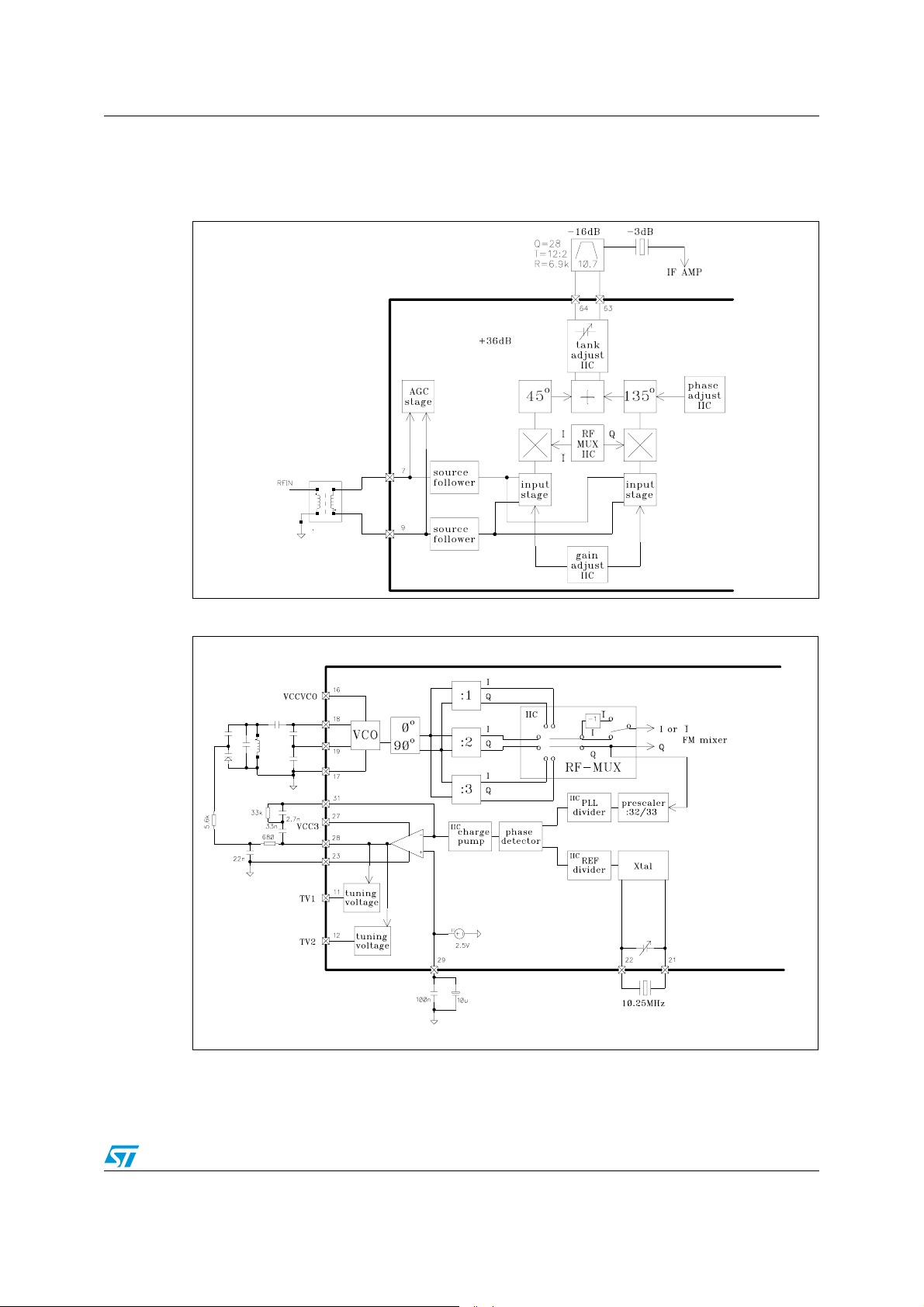
4.1 Mixer 1, AGC and 1.IF
FM quadrature I/Q-mixer converts RF to IF1 of 10.7MHz. The mixer provides inherent image
rejection and wide dynamic range with low noise and large input signal performance. The
mixer1 tank can be adjusted by software (IF1T). For accurate image rejection the gain- and
phase-error generated as well in mixer as VCO stage can be compensated by software
(G,PH)
It is capable of tuning the US FM, US weather, Europe FM, Japan FM and East Europe FM
bands
● US FM = 87.9 to 107.9 MHz
● US weather = 162.4 to 162.55 MHz
● Europe FM = 87.5 to 108 MHz
● Japan FM = 76 to 91 MHz
● East Europe FM = 65.8 to 74 MHz
The AGC operates on different sensitivities and bandwidths in order to improve the input
sensitivity and dynamic range. AGC thresholds are programmable by software
(RFAGC,IFAGC,KAGC). The output signal is a controlled current for double pin diode
attenuator. Two 10.7 MHz programmable amplifiers (IFG1, IFG2) correct the IF ceramic
insertion loss and the costumer level plan application.
4.2 Mixer 2, limiter and demodulator
In this 2. mixer stage the first 10.7 MHz IF is converted into the second 450 kHz IF. A multistage limiter generates signals for the complete integrated demodulator without external
tank. MPX output DC offset versus noise DC level is correctable by software (DEM).
4.3 Quality detection and ISS
4.3.1 Fieldstrength
Parallel to mixer 2 input a 10.7 MHz limiter generates a signal for digital IF counter and a
fieldstrength output signal. This internal unweighted fieldstrength is used for keying AGC,
adjacent channel and multipath detection and is available at PIN14 (FSU) after +6dB buffer
stage. The behaviour of this output signal can be corrected for DC offset (SL) and slope
(SMSL). The internal generated unweighted fieldstrength is filtered at PIN35 and used for
softmute function and generation of ISS filter switching signal for weak input level (sm).
4.3.2 Adjacent channel detector
The input of the adjacent channel detector is AC coupled from internal unweighted
fieldstrength. A programmable highpass or bandpass (ACF) and amplifier (ACG) as well as
rectifier determines the influences. This voltage is compared with adjustable comparator1
thresholds (ACWTH, ACNTH). The output signal of this comparator generates a DC level at
PIN15 by programmable time constant. Time control (TISS) for a present adjacent channel
is made by charge and discharge current after comparator1 in an external capacitance. The
Doc ID 12668 Rev 2 17/45
Page 18

Functional description TDA7512F
charge current is fixed and the discharge current is controlled by I2C Bus. This level
produces digital signals (ac, ac+) in an additional comparator4. The adjacent channel
information is available as analog output signal after rectifier and +8 dB output buffer.
4.3.3 Multipath detector
The input of the multipath detector is AC coupled from internal unweighted fieldstrength. A
programmable bandpass (MPF) and amplifier (MPG) as well as rectifier determines the
influences. This voltage is compared with an adjustable comparator2 thresholds (MPTH).
The output signal of this comparator 2 is used for the "Milano" effect. In this case the
adjacent channel detection is switched off. The "Milano" effect is selectable by I
(MPOFF). The multipath information is available as analog output signal after rectifier and
+8 dB output buffer.
2
C bus
4.3.4 450 kHz IF narrow bandpass filter (ISS filter)
The device gets an additional second IF narrow bandpass filter for suppression of noise and
adjacent channel signal influences. This narrow filter has three switchable bandwidthes,
narrow range of 80 kHz, mid range of 120 kHz and 30 kHz for weather band information.
Without ISS filter the IF bandwidth (wide range) is defined only by ceramic filter chain. The
filter is switched in after mixer 2 before 450 kHz limiter stage. The centre frequency is
matching to the demodulator center frequency.
4.3.5 Deviation detector
In order to avoid distortion in audio output signal the narrow ISS filter is switched OFF for
present overdeviation. Hence the demodulator output signal is detected.
A lowpass filtering and peak rectifier generates a signal that is defined by software
controlled current (TDEV) in an external capacitance. This value is compared with a
programmable comparator3 thresholds (DWTH, DTH) and generates two digital signals
(dev, dev+). For weak signal condition deviation threshold is proportinal to FSU.
4.3.6 ISS switch logic
All digital signals coming from adjacent channel detector, deviation detector and softmute
are acting via switching matrix on ISS filter switch. The IF bandpass switch mode is
controlled by software (ISSON, ISS30, ISS80, CTLOFF).
The switch ON of the IF bandpass is also available by external manipulation of the voltage at
PIN15.
Two application modes are available (APPM). The conditions are described in table 34.
4.4 Soft Mute control
The external fieldstrength signal at PIN 35 is the reference for mute control. The startpoint
and mute depth are programmable (SMTH, SMD) in a wide range. The time constant is
defined by external capacitance. Additional adjacent channel mute function is supported.
A highpass filter with -3 dB threshold frequency of 100 kHz, amplifier and peak rectifier
generates an adjacent noise signal from MPX output with the same time constant for
18/45 Doc ID 12668 Rev 2
Page 19

TDA7512F Functional description
softmute. This value is compared with comparator5 thresholds (ACM). For present strong
adjacent channel the MPX signal is additional attenuated (ACMD).
4.5 PLL and IF counter section
4.5.1 PLL frequency synthesizer block
This part contains a frequency synthesizer and a loop filter for the radio tuning system. Only
one VCO is required to build a complete PLL system for FM world tuning . For auto search
stop operation an IF counter system is available.
The counter works in a two stages configuration. The first stage is a swallow counter with a
two modulus (32/33) precounter. The second stage is an 11-bit programmable counter.
The circuit receives the scaling factors for the programmable counters and the values of the
reference frequencies via an I
2
C bus interface.The reference frequency is generated by an
adjustable internal (XTAL) oscillator followed by the reference divider. The main reference
and step-frequencies are free selectable (RC, PC).
Output signals of the phase detector are switching the programmable current sources. The
loop filter integrates their currents to a DC voltage.
The values of the current sources are programmable by 6 bits also received via the I
(A, B, CURRH).
To minimize the noise induced by the digital part of the system, a special guard
configuration is implemented. The loop gain can be set for different conditions by setting the
current values of the chargepump generator.
4.5.2 Frequency generation for phase comparison
The RF signals applies a two modulus counter (32/33) pre-scaler, which is controlled by a 5bit A-divider. The 5-bit register (PC0 to PC4) controls this divider. In parallel the output of the
prescaler connects to an 11-bit B-divider. The 11-bit PC register (PC5 to PC15) controls this
divider
Dividing range:
f
= [33 x A + (B + 1 - A) x 32] x f
VCO
f
= (32 x B + A + 32) x f
VCO
REF
Important: For correct operation: A ≤ 32; B ≥ A
REF
2
C Bus
4.5.3 Three state phase comparator
The phase comparator generates a phase error signal according to phase difference
between f
SYN
and f
. This phase error signal drives the charge pump current generator.
REF
4.5.4 Charge pump current generator
This system generators signed pulses of current. The phase error signal decides the
duration and polarity of those pulses. The current absolute values are programmable by A
register for high current and B register for low current.
Doc ID 12668 Rev 2 19/45
Page 20

Functional description TDA7512F
4.5.5 Inlock detector
Switching the chargepump in low current mode can be done either via software or
automatically by the inlock detector, by setting bit LDENA to "1".
After reaching a phase difference about lower than 40nsec the chargepump is forced in low
current mode. A new PLL divider alternation by I
high current mode.
4.5.6 Low noise CMOS op-amp
An internal voltage divider at pin VREF2 connects the positive input of the low noise opamp. The charge pump output connects the negative input. This internal amplifier in
cooperation with external components can provide an active filter.
While the high current mode is activated LPHC output is switched on.
4.5.7 IF counter block
The aim of IF counter is to measure the intermediate frequency of the tuner. The input signal
is the 10.7MHz IF level after limiter.
The grade of integration is adjustable by eight different measuring cycle times. The
tolerance of the accepted count value is adjustable, to reach an optimum compromise for
search speed and precision of the evaluation.
4.5.8 Sampling timer
A sampling timer generates the gate signal for the main counter. The basically sampling
time are in FM mode 6.25kHz (t
This is followed by an asynchronous divider to generate several sampling times.
=160μs).
TIM
2
C-Bus will switch the chargepump in the
4.5.9 Intermediate frequency main counter
This counter is a 11 - 21-bit synchronous autoreload down counter. Five bits (CF) are
programmable to have the possibility for an adjust to the centre frequency of the IF-filter.
The counter length is automatic adjusted to the chosen sampling time.
At the start the counter will be loaded with a defined value which is an equivalent to the
divider value (t
SamplexfIF
If a correct frequency is applied to the IF counter frequency input at the end of the sampling
time the main counter is changing its state from 0h to 1FFFFFh.
This is detected by a control logic and an external search stop output is changing from LOW
to HIGH. The frequency range inside which a successful count result is adjustable by the
EW bits.
Counter result succeeded:
t
≥ t
≤ t
CNT
CNT
- t
+ t
ERR
ERR
TIM
t
TIM
Counter result failed:
t
> t
TIM
20/45 Doc ID 12668 Rev 2
CNT
+ t
ERR
).
t
CNT
CF 1696 1++
-------------------------------------=
f
IF
Page 21

TDA7512F Functional description
t
< t
TIM
t
= IF timer cycle time (sampling time)
TIM
t
CNT
t
ERR
The IF counter is only started by inlock information from the PLL part. It is enabled by
software (IFENA).
- t
CNT
ERR
= IF counter cycle time
= discrimination window (controlled by the EW registers)
4.5.10 Adjustment of the measurement sequence time
The precision of the measurements is adjustable by controlling the discrimination window.
This is adjustable by programming the control registers EW.
The measurement time per cycle is adjustable by setting the registers IFS.
4.5.11 Adjust of the frequency value
The center frequency of the discrimination window is adjustable by the control registers CF.
4.6 I2C bus interface
The TDA7512F supports the I2C bus protocol. This protocol defines any device that sends
data onto the bus as a transmitter, and the receiving device as the receiver. The device that
controls the transfer is a master and device being controlled is the slave. The master will
always initiate data transfer and provide the clock to transmit or receive operations.
4.6.1 Data transition
Data transition on the SDA line must only occur when the clock SCL is LOW. SDA transitions
while SCL is HIGH will be interpreted as START or STOP condition.
4.6.2 Start condition
A start condition is defined by a HIGH to LOW transition of the SDA line while SCL is at a
stable HIGH level. This "START" condition must precede any command and initiate a data
transfer onto the bus.
The device continuously monitors the SDA and SCL lines for a valid START and will not
response to any command if this condition has not been met.
4.6.3 Stop condition
A STOP condition is defined by a LOW to HIGH transition of the SDA while the SCL line is at
a stable HIGH level. This condition terminates the communication between the devices and
forces the bus-interface of the device into the initial condition.
4.6.4 Acknowledge
Indicates a successful data transfer. The transmitter will release the bus after sending 8 bits
of data. During the 9
it receive the eight bits of data.
th
clock cycle the receiver will pull the SDA line to LOW level to indicate
Doc ID 12668 Rev 2 21/45
Page 22

Functional description TDA7512F
4.6.5 Data transfer
During data transfer the device samples the SDA line on the leading edge of the SCL clock.
Therefore, for proper device operation the SDA line must be stable during the SCL LOW to
HIGH transition.
4.6.6 Device addressing
To start the communication between two devices, the bus master must initiate a start
instruction sequence, followed by an eight bit word corresponding to the address of the
device it is addressing.
The most significant 6 bits of the slave address are the device type identifier.
The TDA7512F device type is fixed as "110001".
The next significant bit is used to address a particular device of the previous defined type
connected to the bus.
The state of the hardwired PIN 41 defines the state of this address bit. So up to two devices
could be connected on the same bus. When PIN 41 is connected to VCC2 the address bit
“1” is selected. When PIN 41 is left open the address bit “0” is selected. Therefor a double
FM tuner concept is possible.
The last bit of the start instruction defines the type of operation to be performed:
– When set to "1", a read operation is selected
– When set to "0", a write operation is selected
The TDA7512F connected to the bus will compare their own hardwired address with the
slave address being transmitted, after detecting a START condition. After this comparison,
the TDA7512F will generate an "acknowledge" on the SDA line and will do either a read or a
write operation according to the state of R/W bit.
4.6.7 Write operation
Following a START condition the master sends a slave address word with the R/W bit set to
"0". The device will generate an "acknowledge" after this first transmission and will wait for a
second word (the word address field). This 8-bit address field provides an access to any of
the 32 internal addresses.
Upon receipt of the word address the TDA7512F slave device will respond with an
"acknowledge". At this time, all the following words transmitted to the TDA7512F will be
considered as Data.
The internal address will be automatically incremented. After each word receipt the
TDA7512F will answer with an "acknowledge".
4.6.8 Read operation
If the master sends a slave address word with the R/W bit set to "1", the TDA7512F will
transit one 8-bit data word. This data word includes the following informations:
bit0 (ISS filter, 1 = ON, 0 = OFF)
bit1 (ISS filter bandwidth, 1 = 80kHz, 0 = 120kHz)
bit2 (MPOUT,1 = multipath present, 0 = no multipath)
22/45 Doc ID 12668 Rev 2
Page 23

TDA7512F Functional description
bit3 (1 = PLL is locked in , 0 = PLL is locked out).
bit4 (fieldstrength indicator, 1 = lower as softmute threshold, 0 = higher as softmute threshold)
bit5 (adjacent channel indicator, 1 = adjacent channel present, 0 = no adjacent channel)
bit6 (deviation indicator, 1 = strong overdeviation present, 0 = no strong overdeviation)
bit7 (deviation indicator, 1 = overdeviation present, 0 = no overdeviation)
Doc ID 12668 Rev 2 23/45
Page 24
Software specification TDA7512F
5 Software specification
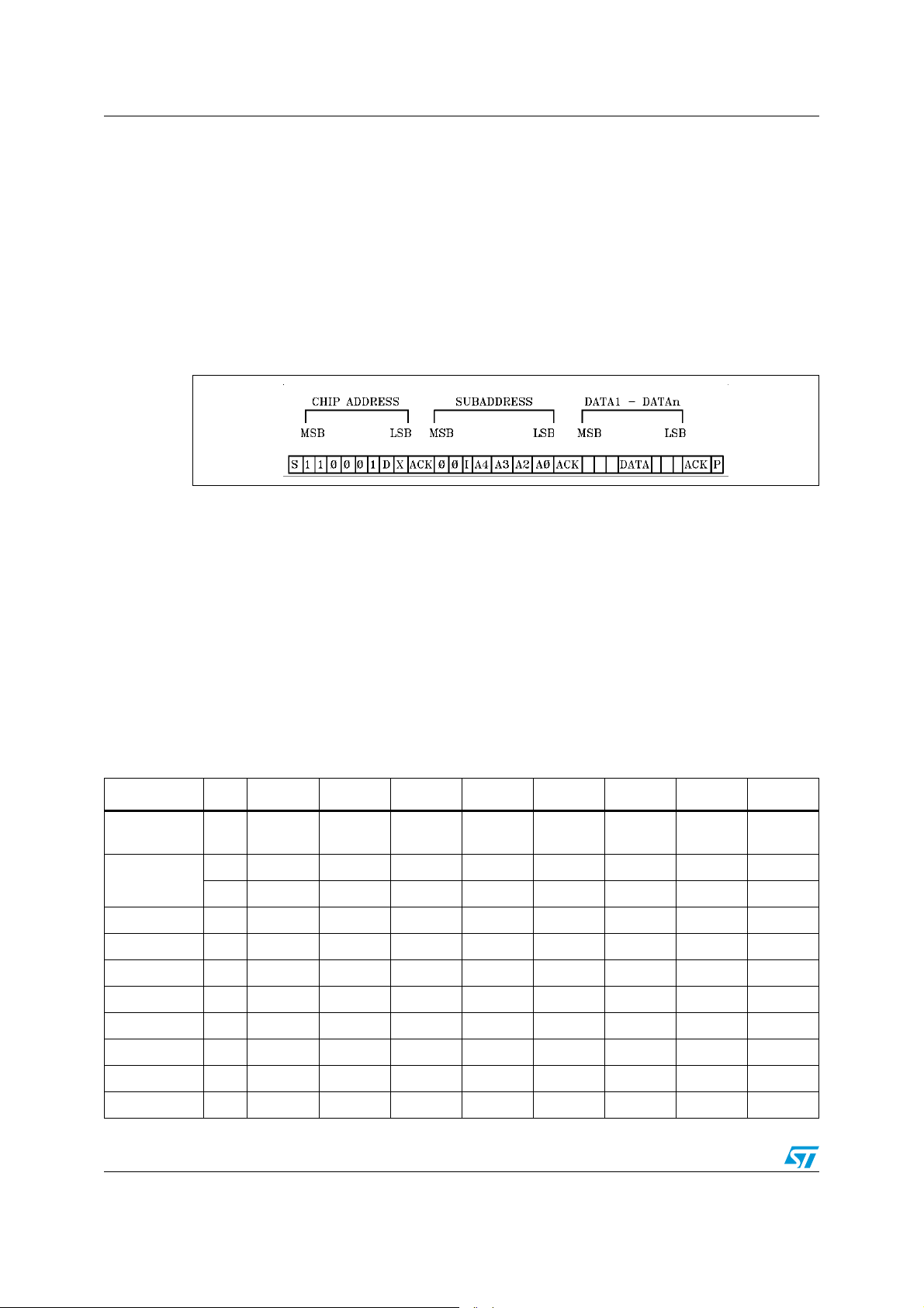
The interface protocol comprises:
– start condition (S)
– chip address byte
– subaddress byte
– sequence of data (N bytes + Acknowledge)
– stop condition (P)
Figure 3. Interface protocol
S = Start
P = Stop
ACK = Acknowledge
D = Device Address
X = R/W bit
I = Pagemode
A = Subaddress
5.1 Address organization
Table 6. Address organization
FunctionAddr76543210
CHARGEPU
MP
PLL
COUNTER
TV1 3 TV1O7 TV1O6 TV1O5 TV1O4 TV1O3 TV1O2 TV1O1 TV1O0
TV2 4 TV2O7 TV2O6 TV2O5 TV2O4 TV2O3 TV2O2 TV2O1 TV2O0
IFC CTRL 1 5 LM CASF - - IFENA IFS2 IFS1 IFS0
IFC CTRL 2 6 EW2 EW1 EW0 CF4 CF3 CF2 CF1 CF0
not valid7--------
QUALITYISS 8 TISS2 TISS1 TISS0 TVWB ISS30 ISS80 ISSON CTLOFF
0 LDENA CURRH B1 B0 A3 A2 A1 A0
1 PC7 PC6 PC5 PC4 PC3 PC2 PC1 PC0
2 PC15 PC14 PC13 PC12 PC11 PC10 PC9 PC8
QUALITY AC 9 ACNTH1 ACNTH0 ACWTH2 ACWTH1 ACWTH0 ACG ACF -
QUALITY MP 10 MPAC APPM2 APPM1 MPTH1 MPTH0 MPG MPF MPOFF
24/45 Doc ID 12668 Rev 2
Page 25
TDA7512F Software specification
Table 6. Address organization (continued)
FunctionAddr76543210
QUALITYDEV 11 BWCTL DTH1 DTH0 DWTH1 DWTH0 TDEV2 TDEV1 TDEV0
MUTE1 12 MENA SMD3 SMD2 SMD1 SMD0 SMTH2 SMTH1 SMTH0
MUTE2 13 F100K ACM3 ACM2 ACM1 ACM0 ACMD1 ACMD0 SMCTH
VCO/PLLREF 14 - - RC2 RC1 RC0 VCOD2 VCOD1 VCOD0
FMAGC 15 - KAGC2 KAGC1 KAGC0 IFAGC1 IFAGC0 RFAGC1 RFAGC0
not valid16--------
DEM ADJ 17 DNB1 DNB0 DEM5 DEM4 DEM3 DEM2 DEM1 DEM0
LEVEL 18 ODSW - SMSL SL4 SL3 SL2 SL1 SL0
IF1/XTAL 19 XTAL4 XTAL3 XTAL2 XTAL1 XTAL0 IFG11 IFG10 IFG2
TANK ADJ 20 IF1T3 IF1T2 IF1T1 IF1T0 - - - -
I/Q ADJ 21 ODCUR - G1 G0 PH3 PH2 PH1 PH0
TESTCTRL1 22 - ISSIN TOUT TIN CLKSEP TEST3 TEST2 TEST1
TESTCTRL2 23 OUT7 OUT6 OUT5 OUT4 OUT3 OUT2 OUT1 OUT0
TESTCTRL3 24 - TINACM TINMP TINAC OUT11 OUT10 OUT9 OUT8
TESTCTRL4 25 - - - OUT16 OUT15 OUT14 OUT13 OUT12
5.2 Control register function
Table 7. Control register function
Register Name Function
A Charge pump high current
ACF Adjacent channel filter select
ACG Adjacent channel filter gain
ACM Threshold for startpoint adjacent channel mute
ACMD Adjacent channel mute depth
ACNTH Adjacent channel narrow band threshold
ACWTH Adjacent channel wide band threshold
APPM Application mode quality detection
B Charge pump low current
BWCTL ISS filter fixed bandwith (ISS80) in automatic control
CASF Check alternative station frequency
CF Center frequency IF counter
CLKSEP Clock separation (only for testing)
CTLOFF Switch off automatic control of ISS filter
CURRH Set current high charge pump
Doc ID 12668 Rev 2 25/45
Page 26

Software specification TDA7512F
Table 7. Control register function (continued)
Register Name Function
DEM Demodulator offset
DNB Demodulator noise spike blanking
DTH Deviation detector threshold for ISS filter “OFF”
DWTH Deviation detector threshold for ISS filter narrow/wide
EW Frequency error window IF counter
F100K Corner frequency of AC-mute high pass filter
G I/Q mixer gain adjust
IF1T Miixer1 tank adjust
IFAGC IF AGC
IFENA IF counter enable
IFG IF1 amplifier gain (10.7MHz)
IFS IF counter sampling time
ISSIN Test input for ISS filter
ISSON ISS filter “ON”
ISS30 ISS filter 30KHz weather band
ISS80 ISS filter narrow/mid switch
KAGC Keying AGC
LDENA Lock detector enable
LM Local mode seek stop
MENA Softmute enable
MPAC Adjacent channel control by multipath
MPF Multipath filter frequency
MPG Multipath filter gain
MPOFF Multipath control “OFF”
MPTH Multipath threshold
ODCUR Current for overdeviation-correction
ODSW Overdeviation-correction enable
OUT Test output (only for testing)
PC Counter for PLL (VCO frequency)
PH I/Q mixer phase adjust
RC Reference counter PLL
RFAGC RF AGC
SL S meter slider
SMCTH Softmute capacitor threshold for ISS “ON”
SMD Softmute depth threshold
26/45 Doc ID 12668 Rev 2
Page 27

TDA7512F Software specification
Table 7. Control register function (continued)
Register Name Function
SMSL S meter slope
SMTH Softmute startpoint threshold
TDEV Time constant for deviation detector
TEST Testing PLL/IFC (only for testing)
TIN Switch FSU PIN to TEST input (only for testing)
TINAC Test input adjacent channel (only for testing)
TINACM Test input adjacent channel mute (only for testing)
TINMP Test input multipath(only for testing)
TISS Time constant for ISS filter “ON”/”OFF”
TOUT Switch FSU PIN to Test output (only for testing)
TVO Tuning voltage offset for prestage
TVWB Tuning voltage offset for prestage (weather band mode)
VCOD VCO divider
XTAL Xtal frequency adjust
Table 8. Subaddress
MSB LSB
- - I A4A3A2A1A0
- - -00000Charge pump control
- - -00001PLL lock detector
---------
- - -10101I/Q ADJ
--0-----Page mode “OFF”
--1-----Page mode enable
5.3 Data byte specification
Table 9. Addr 0 charge pump control
MSB LSB
d7 d6 d5 d4 d3 d2 d1 d0
- - - - 0 0 0 0 High current = 0 mA
- - - - 0 0 0 1 High current = 0.5 mA
- - - - 0 0 1 0 High current = 1 mA
Function
Function
- - - - 0 0 1 1 High current = 1.5 mA
---------
Doc ID 12668 Rev 2 27/45
Page 28
Software specification TDA7512F
Table 9. Addr 0 charge pump control (continued)
MSB LSB
Function
d7 d6 d5 d4 d3 d2 d1 d0
- - - - 1 1 1 1 High current = 7.5 mA
--00----Low current = 0 µA
- - 0 1 - - - - Low current = 50 µA
- - 1 0 - - - - Low current = 100 µA
- - 1 1 - - - - Low current = 150 µA
-0------Select low current
-1------Select high current
0 - - - - - - - Lock detector disable
1-------Lock detector enable
Table 10. Addr 1 PLL counter 1 (LSB)
MSB LSB
d7 d6 d5 d4 d3 d2 d1 d0
00000000LSB = 0
00000001LSB = 1
00000010LSB = 2
---------
11111100LSB = 252
11111101LSB = 253
11111110LSB = 254
11111111LSB = 255
Table 11. Addr 2 PLL counter 2 (MSB)
MSB LSB
d7 d6 d5 d4 d3 d2 d1 d0
00000000MSB = 0
00000001MSB = 256
Function
Function
00000010MSB = 512
---------
11111100MSB = 64768
11111101MSB = 65024
11111110MSB = 65280
11111111MSB = 65536
Note: Swallow mode: f
VCO/fSYN
= LSB + MSB + 32
28/45 Doc ID 12668 Rev 2
Page 29

TDA7512F Software specification
Table 12. Addr 3,4 TV1,2 (offset refered to tuning voltage PIN 28)
MSB LSB
d7 d6 d5 d4 d3 d2 d1 d0
-0000000Tuning Voltage Offset = 0
-0000001TVO = 25mV
-0000010TVO = 50mV
---------
-1111111TVO = 3175mV
0--------TVO
1-------+TVO
Table 13. Addr 5 IF counter control 1
MSB LSB
d7 d6 d5 d4 d3 d2 d1 d0
-----000t
-----001t
-----010t
-----011t
-----100t
-----101t
-----110t
-----111t
= 20.48 ms (FM)128 ms (AM )
Sample
= 10.24 ms (FM)64 ms (AM )
Sample
= 5.12 ms (FM)32 ms (AM )
Sample
= 2.56 ms (FM)16 ms (AM )
Sample
= 1.28 ms (FM)8 ms (AM )
Sample
= 640 µs (FM)4 ms (AM )
Sample
= 320 µs (FM)2 ms (AM)
Sample
= 160 µs (FM)1 ms (AM )
Sample
- - - - 0 - - - IF counter disable / stand by
Function
Function
- - - - 1 - - - IF counter enable
--01----has to be set
- 0 - - - - - - Disable mute & AGC on hold
-1------Enable mute & AGC on hold
0 - - - - - - - Disable local mode
1 - - - - - - - Enable local mode (PIN diode current = 0.5 mA) “ON”
Table 14. Addr 6 IF Counter Control 2
MSB LSB
Function
d7 d6 d5 d4 d3 d2 d1 d0
- - - 00000f
- - - 00001f
= 10.60625 MHz
Center
= 10.61250 MHz
Center
---------
- - - 01011f
= 10.67500 MHz
Center
Doc ID 12668 Rev 2 29/45
Page 30

Software specification TDA7512F
Table 14. Addr 6 IF Counter Control 2 (continued)
MSB LSB
Function
d7 d6 d5 d4 d3 d2 d1 d0
- - - 01100f
- - - 01101f
- - - 01110f
- - - 01111f
= 10.68125 MHz
Center
= 10.68750 MHz
Center
= 10.69375 MHz
Center
= 10.70000 MHz
Center
---------
- - - 11111f
= 10.80000 MHz
Center
000-----Not valid
001-----Not valid
010-----Not valid
011-----Δf = 6.25kHz
100-----
101-----
110-----
111-----
Table 15. Addr 7 not valid
Δf = 12.5kHz
Δf = 25kHz
Δf = 50kHz
Δf = 100kHz
MSB LSB
d7 d6 d5 d4 d3 d2 d1 d0
Function
00000000 has to be set
Table 16. Addr 8 quality ISS filter
MSB LSB
Function
d7 d6 d5 d4 d3 d2 d1 d0
- ------0ISS filter control “ON”
------1ISS filter control “OFF”
- -----0-Switch ISS filter “OFF”
- -----1-Switch ISS filter “ON”
- - - - - 0 - - Switch “OFF” ISS filter 120kHz
- - - - - 1 - - Switch “ON” ISS filter 80kHz
- - - - 0 - - - Switch “OFF” ISS filter 30KHz for weatherband
- - - - 1 - - - Switch “ON” ISS filter 30KHz for weatherband
- - - 0 - - - - Disable TV offset for weather band
- - - 1 - - - - Enable TV offset for weather band (+4V)
000-----discharge current1
μA, charge current mid 74μΑ narrow124μΑ
30/45 Doc ID 12668 Rev 2
Page 31

TDA7512F Software specification
Table 16. Addr 8 quality ISS filter (continued)
MSB LSB
Function
d7 d6 d5 d4 d3 d2 d1 d0
001-----
010-----
011-----
discharge current 3µA, charge current mid 72µA narrow 122µA
discharge current 5µA, charge current mid 70 µA narrow 120µA
discharge current 7µA, charge current mid 68µA narrow 118µA
- ------ --
111-----
Table 17. Addr 9 quality detection adjacent channel
discharge current 15µA,charge current mid 60µA narrow 110µA
MSB LSB
Function
d7 d6 d5 d4 d3 d2 d1 d0
-------0/1Not valid
- - - - - - 0 - AC highpass frequency 100 kHz
- - - - - - 1 - AC bandpass frequency 100 kHz
- - - - - 0 - - AC gain 32 dB
- - - - - 1 - - AC gain 38 dB
- - 0 0 0 - - - AC wide band threshold 0.25 V
- - 0 0 1 - - - AC wide band threshold 0.35 V
- - 0 1 0 - - - AC wide band threshold 0.45 V
---------
- - 1 1 1 - - - AC wide band threshold 0.95 V
0 0 - - - - - - AC narrow band threshold 0.0 V
0 1 - - - - - - AC narrow band threshold 0.1 V
1 0 - - - - - - AC narrow band threshold 0.2 V
1 1 - - - - - - AC narrow band threshold 0.3 V
Table 18. Addr 10 quality detection multipath
MSB LSB
d7 d6 d5 d4 d3 d2 d1 d0
-------0Multipath control “ON”
-------1Multipath control “OFF”
------0-MP bandpass frequency 19 kHz
------1-MP bandpass frequency 31 kHz
-----0--MP gain 12 dB
-----1--MP gain 23 dB
- - - 0 0 - - - MP threshold 0.50 V
Function
Doc ID 12668 Rev 2 31/45
Page 32
Software specification TDA7512F
Table 18. Addr 10 quality detection multipath (continued)
MSB LSB
Function
d7 d6 d5 d4 d3 d2 d1 d0
- - - 0 1 - - - MP threshold 0.75 V
- - - 1 0 - - - MP threshold 1.00 V
- - - 1 1 - - - MP threshold 1.25 V
-00-----Application mode 1
-01-----Application mode 2
0-------Multipath eliminates ac
1-------Multipath eliminates ac and ac+
Table 19. Addr 11 quality deviation detection
MSB LSB
Function
d7 d6 d5 d4 d3 d2 d1 d0
- ----000charge current 34 µA
- ----001charge current 32 µA
- ----010charge current 30 µA
- ----011charge current 28 µA
, discharge current 6 µA
, discharge current 8 µA
, discharge current 10 µA
, discharge current 12 µA
- --------
- ----111charge current 20 µA, discharge current 20 µA
- - - 0 0 - - - DEV threshold for ISS narrow/wide 30 kHz
- - - 0 1 - - - DEV threshold for ISS narrow/wide 45 kHz
- - - 1 0 - - - DEV threshold for ISS narrow/wide 60 kHz
- - - 1 1 - - - DEV threshold for ISS narrow/wide 75 kHz
- 00-----DEV threshold for ISS filter “OFF” ratio 1.5
- 01-----DEV threshold for ISS filter “OFF” ratio 1.4
- 10-----DEV threshold for ISS filter “OFF” ratio 1.3
- 11-----DEV threshold for ISS filter “OFF” ratio 1
0 -------
Disable ISS filter to fixed bandwith (ISS80) in automatic
control
1 -------
Table 20. Addr 12 soft mute control 1
Enable ISS filter to fixed bandwith (ISS80) in automatic
control
MSB LSB
Function
d7 d6 d5 d4 d3 d2 d1 d0
- - - - - 0 0 0 Startpoint mute 0 in application about 3dBµV antenna level
- - - - - 0 0 1 Startpoint mute 1in application about 4dBµV antenna level
32/45 Doc ID 12668 Rev 2
Page 33

TDA7512F Software specification
Table 20. Addr 12 soft mute control 1 (continued)
MSB LSB
Function
d7 d6 d5 d4 d3 d2 d1 d0
---------
- - - - - 1 1 1 Startpoint mute 7in application about 10dB
- 0 0 0 0 - - - Mute depth 0 in application 18d B
- 0 0 0 1 - - - Mute depth 1 in application 20 dB
- 0 0 1 0 - - - Mute depth 2 in application 22 dB
- 0 0 1 1 - - - Mute depth 3 in application 24 dB
- - - - - - - - - (logarithmically behaviour)
- 1 1 1 1 - - - Mute depth 15 in application 36 dB
0 - - - - - - - Mute disable
1 - - - - - - - Mute enable
Table 21. Addr 13 soft mute control 2
MSB LSB
Function
d7 d6 d5 d4 d3 d2 d1 d0
-------0Disable mute threshold for ISS filter “ON”
-------1Enable mute threshold for ISS filter “ON”
- - - - - 0 0 - AC mute depth 10 dB
- - - - - 0 1 - AC mute depth 8 dB
- - - - - 1 0 - AC mute depth 6 dB
- - - - - 1 1 - AC mute depth 4 dB
-0000 - - -AC mute threshold 60 mV
μV antenna level
-0001 - - -AC mute threshold 80 mV
-0010 - - -AC mute threshold 100 mV
---------
-0111 - - -AC mute threshold 340 mV
-1111 - - -AC mute “OFF”
0-------AC mute filter 110 kHz
1-------AC mute filter 100 kHz
Table 22. Addr 14 VCODIV/PLLREF
MSB LSB
Function
d7 d6 d5 d4 d3 d2 d1 d0
- - - - - - 0 0 not valid (only for testing)
- - - - - - 0 1 VCO frequency divided by 2
Doc ID 12668 Rev 2 33/45
Page 34

Software specification TDA7512F
Table 22. Addr 14 VCODIV/PLLREF (continued)
MSB LSB
Function
d7 d6 d5 d4 d3 d2 d1 d0
- - - - - 1 0 VCO frequency divided by 3
- - - - - 1 1 original VCO frequency
-----0--VCO” I” signal 0 °C
- - - - - 1 - - VCO “I” signal 180 °C
- - 1 0 0 - - - PLL reference frequency 50 kHz
- - 1 0 1 - - - PLL reference frequency 25 kHz
- - 1 1 0 - - - PLL reference frequency 10 kHz
- - 1 1 1 - - - PLL reference frequency 9 kHz
- - 0 0 0 - - - PLL reference frequency 2 kHz
0 0 - - - - - - has to be set
Table 23. Addr 15 FM AGC
MSB LSB
d7 d6 d5 d4 d3 d2 d1 d0
------00RFAGC threshold V
------01RFAGC threshold V
------10RFAGC threshold V
------11RFAGC threshold V
- - - - 0 0 - - IFAGC threshold V
- - - - 0 1 - - IFAGC threshold V
- - - - 1 0 - - IFAGC threshold V
- - - - 1 1 - - IFAGC threshold V
- 0 0 0 - - - - KAGC threshold 80 dBµV
- 0 0 1 - - - - KAGC threshold 82 dBµV
- 0 1 0 - - - - KAGC threshold 84 dBµV
- 0 1 1 - - - - KAGC threshold 86 dBµV
- 1 0 0 - - - - KAGC threshold 88 dBµV
- 1 0 1 - - - - KAGC threshold 90 dBµV
Function
= 85 (77 ANT) dBµV
7-9TH
= 90 (82 ANT) dBµV
7-9TH
= 94 (86 ANT) dBµV
7-9TH
= 96 (88 ANT) dBµV
7-9TH
= 86 (60 ANT) dBµV
60TH
= 92 (66 ANT) dBµV
60TH
= 96 (70 ANT) dBµV
60TH
= 98 (72 ANT) dBµV
60TH
- 1 1 0 - - - - KAGC threshold 92 dBµV
-111 - - - -Keying AGC “OFF”
0-------has to be “0”
34/45 Doc ID 12668 Rev 2
Page 35

TDA7512F Software specification
Table 24. Addr 16 not valid
MSB LSB
d7 d6 d5 d4 d3 d2 d1 d0
11111111has to be set
Table 25. Addr 17 FM demodulator fine adjust
MSB LSB
d7 d6 d5 d4 d3 d2 d1 d0
- -0000000 mV
- -000001+8.5 mV
- -000010+17 mV
---------
- -011111+263.5 mV
- -1000000 mV
- -100001-8.5 mV
- -100010-17 mV
---------
Function
Function
- -111111-263.5 mV
00------Spike cancelation ”OFF”
01------Threshold for spike cancelation 270 mV
10------Threshold for spike cancelation 520 mV
11------Threshold for spike cancelation 750 mV
Table 26. Addr 18 s-meter slider
MSB LSB
Function
d7 d6 d5 d4 d3 d2 d1 d0
- - - - 0 0 0 0 S meter slider offset SL=0dB
- - - - 0 0 0 1 S meter offset SL=1dB
- - - - 0 0 1 0 S meter offset SL=2dB
---------
- - - - 1 1 1 1 S meter offset SL=15dB
---0----S meter offset -SL
---1----S meter offset +SL
--0-----S Meter slope 1 V/decade
--1-----S meter slope 1.5 V/decade
-1------has to be set
Doc ID 12668 Rev 2 35/45
Page 36

Software specification TDA7512F
Table 26. Addr 18 s-meter slider (continued)
MSB LSB
Function
d7 d6 d5 d4 d3 d2 d1 d0
0-------Overdeviation correction “ON”
1-------Overdeviation correction “OFF”
Table 27. Addr 19 IF GAIN/XTAL adjust
MSB LSB
d7 d6 d5 d4 d3 d2 d1 d0
-------0IF1 gain2 9d B
- - - - - - - 1 IF1 gain2 11 dB
- - - - - 0 0 - IF1 gain1 9 dB
- - - - - 0 1 - IF1 gain1 11 dB
- - - - - 1 0 - IF1 gain1 12 dB
- - - - - 1 1 - IF1 gain1 15 dB
00000 - - -C
00001 - - -C
00010 - - -C
00011 - - -C
00100 - - -C
Load
Load
Load
Load
Load
0 pF
0.75 pF
1.5 pF
2.25 pF
3 pF
---------
11111 - - -C
Table 28. Addr 20 tank adjust
Load
23.25 pF
Function
MSB LSB
d7 d6 d5 d4 d3 d2 d1 d0
- - - - 0 0 0 0 has to be set
0 0 0 0 - - - - 10.7 MHz 0 pF
0 0 0 1 - - - - 10.7 MHz 0.55 pF
0 0 1 0 - - - - 10.7 MHz 1.1 pF
0 0 1 1 - - - - 10.7 MHz 1.65 pF
---------
1 1 1 1 - - - - 10.7 Hz 8.25 pF
36/45 Doc ID 12668 Rev 2
Function
Page 37

TDA7512F Software specification
Table 29. Addr 21 I/Q mixer 1 adjust
MSB LSB
Function
d7 d6 d5 d4 d3 d2 d1 d0
----0000-7 °C
----0001-6 °C
----0010-5 °C
---------
----01110 °C
----1000+1 °C
----1001+2 °C
---------
----1111+8 °C
--00----0 %
--01-----1 %
--10----+1 %
--11----0 %
-x------not used
0 - - - - - - - Overdeviation correction current max = 45 µA
1 - - - - - - - Overdeviation correction current max = 90 µA
Table 30. Addr 22 test control 1
MSB LSB
Function
d7 d6 d5 d4 d3 d2 d1 d0
xxxxxxxxOnly for testing ( have to be set to 0)
Table 31. Addr 23 test control 2
MSB LSB
Function
d7 d6 d5 d4 d3 d2 d1 d0
xxxxxxxxOnly for testing ( have to be set to 0)
Table 32. Addr 24 Test control 3
MSB LSB
Function
d7 d6 d5 d4 d3 d2 d1 d0
xxxxxxxxOnly for testing ( have to be set to 0)
Table 33. Addr 25 test control 4
MSB LSB
Function
d7 d6 d5 d4 d3 d2 d1 d0
x x x x x x x x Only for testing ( have to be set to 0)
Doc ID 12668 Rev 2 37/45
Page 38

Package information TDA7512F
6 Package information
In order to meet environmental requirements, ST offers these devices in different grades of
ECOPACK
®
packages, depending on their level of environmental compliance. ECOPACK
®
specifications, grade definitions and product status are available at: www.st.com.
ECOPACK
®
is an ST trademark.
Figure 4. LQFP64 mechanical data and package dimensions
DIM.
A 1.60 0.063
A1 0.05 0.15 0.002 0.006
A2 1.35 1.40 1.45 0.053 0.055 0.057
B 0.17 0.22 0.27 0.0066 0.0086 0.0106
C 0.09 0 .0035
D 11.80 12.00 12.20 0.464 0.472 0.480
D1 9.80 10.00 10.20 0.386 0.394 0.401
D3 7.50 0.295
e 0.50 0.0197
E 11.80 12.00 12.20 0.464 0.472 0.480
E1 9.80 10.00 10.20 0.386 0.394 0.401
E3 7.50 0.295
L 0.45 0.60 0.75 0.0177 0.0236 0.0295
L1 1.00 0.0393
K 0˚ (m in.), 3.5˚ (typ.), 7˚ (max.)
ccc 0.080 0.0031
mm inch
MIN. TYP. MAX. MIN. TYP. MAX.
OUTLINE AND
MECHANICAL DATA
LQFP64 (10 x 10 x 1.4mm)
D
D1
48
49
B
64
1
e
33
32
E3D3E1
17
16
38/45 Doc ID 12668 Rev 2
A
A2
A1
0.08mm
ccc
Seating Plane
B
E
C
L1
L
K
0051434 F
Page 39
TDA7512F Block diagrams
Appendix A Block diagrams
Figure 5. Block diagram I/Q mixer
Figure 6. Block diagram VCO
Doc ID 12668 Rev 2 39/45
Page 40

Block diagrams TDA7512F
Figure 7. Block diagram keying AGC
Figure 8. Block diagram ISS function
40/45 Doc ID 12668 Rev 2
Page 41
TDA7512F Block diagrams
Table 34. Block diagram quality detection principle (without overdeviation
correction)
Signal Low High
ac No adjacent channel Adjacent channel present
ac+ No strong adjacent channel Adjacent channel higher as ac
sm
Fieldstrength higher as softmute
threshold
dev Deviation lower as threshold DWTH Deviation higher as threshold DWTH
dev+
Deviation lower as threshold
DTH*DWTH
inton ISS filter off by logic (wide) ISS filter on by logic
int80 ISS filter 120kHz (mid) ISS filter 80kHz (narrow)
Table 35. Input signals modes
Input signals Mode 1 Mode 2
0ac 0ac+ 0sm 0dev 0dev+ 0inton 0int80 0Function 0inton 0int80 0Function
000000 0wide00wide
000100 0wide00wide
Fieldstrength lower as softmute
threshold
Deviation higher as threshold
DTH*DWTH
000110 0wide00wide
001001 1narrow11narrow
001100 0wide10mid
001110 0wide00wide
100001 1narrow10mid
110001 1narrow11narrow
100101 0 mid 10mid
110111 0 mid 11narrow
101001 1narrow11narrow
111001 1narrow11narrow
101101 0 mid 10mid
111101 0 mid 11narrow
101111 0 mid 10mid
111111 0 mid 11narrow
Doc ID 12668 Rev 2 41/45
Page 42

Block diagrams TDA7512F
Table 36. Part list (application- and measurment circuit)
Item Description
F1 TOKO 5KM 396INS-A542EK
F2 TOKO MC152 E558CN-100021
F3 TOKO 7PSG 826RC-5134N
L1 TOKO LQH31
L2 TOKO LL 2012-680
CF1 TOKO CFSK107M3-AE-20X
CF2 TOKO CFSK107M4-AE-20X
D1,D2 TOKO KP2311E
D3 TOKO KV1370NT
D4 PHILIPS BB156
Figure 9. Application circuit
42/45 Doc ID 12668 Rev 2
Page 43

TDA7512F Application notes
Appendix B Application notes
Following items are important to get highest performance of TDA7512F in application:
1. In order to avoid leakage current from PLL loop filter input to ground a guardring is
recommended around loop filter PIN’s with PLL reference voltage potential.
2. Distance between Xtal and VCO input PIN 18 should be far as possible and Xtal
package should get a shield versus ground.
3. Blocking of VCO supply should be near at PIN 16 and PIN 17.
4. Wire lenght to FM mixer1 input and output should be symetrically and short.
5. FM demodulator capacitance at PIN 44 should be sense connected as short as
possible versus demodulator ground at PIN 47.
6. With respect to THD capacitive coupling from PIN 20 to VCO should be avoided.
Capacitance at PIN 20 has be connected versus VCC2 ground.
Doc ID 12668 Rev 2 43/45
Page 44

Revision history TDA7512F
7 Revision history
Table 37. Document revision history
Date Revision Changes
05-Sep-2006 1 Initial release.
24-Jun-2009 2 Updated Section 6: Package information on page 38.
44/45 Doc ID 12668 Rev 2
Page 45

TDA7512F
Please Read Carefully:
Information in this document is provided solely in connection with ST products. STMicroelectronics NV and its subsidiaries (“ST”) reserve the
right to make changes, corrections, modifications or improvements, to this document, and the products and services described herein at any
time, without notice.
All ST products are sold pursuant to ST’s terms and conditions of sale.
Purchasers are solely responsible for the choice, selection and use of the ST products and services described herein, and ST assumes no
liability whatsoever relating to the choice, selection or use of the ST products and services described herein.
No license, express or implied, by estoppel or otherwise, to any intellectual property rights is granted under this document. If any part of this
document refers to any third party products or services it shall not be deemed a license grant by ST for the use of such third party products
or services, or any intellectual property contained therein or considered as a warranty covering the use in any manner whatsoever of such
third party products or services or any intellectual property contained therein.
UNLESS OTHERWISE SET FORTH IN ST’S TERMS AND CONDITIONS OF SALE ST DISCLAIMS ANY EXPRESS OR IMPLIED
WARRANTY WITH RESPECT TO THE USE AND/OR SALE OF ST PRODUCTS INCLUDING WITHOUT LIMITATION IMPLIED
WARRANTIES OF MERCHANTABILITY, FITNESS FOR A PARTICULAR PURPOSE (AND THEIR EQUIVALENTS UNDER THE LAWS
OF ANY JURISDICTION), OR INFRINGEMENT OF ANY PATENT, COPYRIGHT OR OTHER INTELLECTUAL PROPERTY RIGHT.
UNLESS EXPRESSLY APPROVED IN WRITING BY AN AUTHORIZED ST REPRESENTATIVE, ST PRODUCTS ARE NOT
RECOMMENDED, AUTHORIZED OR WARRANTED FOR USE IN MILITARY, AIR CRAFT, SPACE, LIFE SAVING, OR LIFE SUSTAINING
APPLICATIONS, NOR IN PRODUCTS OR SYSTEMS WHERE FAILURE OR MALFUNCTION MAY RESULT IN PERSONAL INJURY,
DEATH, OR SEVERE PROPERTY OR ENVIRONMENTAL DAMAGE. ST PRODUCTS WHICH ARE NOT SPECIFIED AS "AUTOMOTIVE
GRADE" MAY ONLY BE USED IN AUTOMOTIVE APPLICATIONS AT USER’S OWN RISK.
Resale of ST products with provisions different from the statements and/or technical features set forth in this document shall immediately void
any warranty granted by ST for the ST product or service described herein and shall not create or extend in any manner whatsoever, any
liability of ST.
ST and the ST logo are trademarks or registered trademarks of ST in various countries.
Information in this document supersedes and replaces all information previously supplied.
The ST logo is a registered trademark of STMicroelectronics. All other names are the property of their respective owners.
© 2009 STMicroelectronics - All rights reserved
STMicroelectronics group of companies
Australia - Belgium - Brazil - Canada - China - Czech Republic - Finland - France - Germany - Hong Kong - India - Israel - Italy - Japan -
Malaysia - Malta - Morocco - Philippines - Singapore - Spain - Sweden - Switzerland - United Kingdom - United States of America
www.st.com
Doc ID 12668 Rev 2 45/45
 Loading...