

TDA7468
Fi
TWO BANDS DIGITALLY CONTROLLED
AUDIO PROCESSOR WITH BASS ALC SURROUND
1 FEATURES
INPUT MULTIPLEXER
– 4 STEREO INPUTS
– SELECTABLE INPUT GAIN FOR OPTIMAL
ADAPTATION TO DIFFERENT SOURCES
ONE STEREO OUTPUT
BASS ALC
TREBLE AND BASS CONTROL IN 2.0dB
STEPS
VOLUME CONTROL IN 1.0dB STEPS
TWO SPEAKER ATTENUATORS:
– TWO INDEPENDENT SPEAKER CONTROL
IN 1.0dB STEPS FOR BALANCE FACILITY
– INDEPENDENT MUTE FUNCTION
ALL FUNCTION ARE PROGRAMMABLE VIA
SERIAL BUS
EXTERNALLY ADJUSTABLE SURROUND
2 DESCRIPTION
The TDA7468D is a volume tone (bass and treble)
balance (Left/Right) processor for quality audio
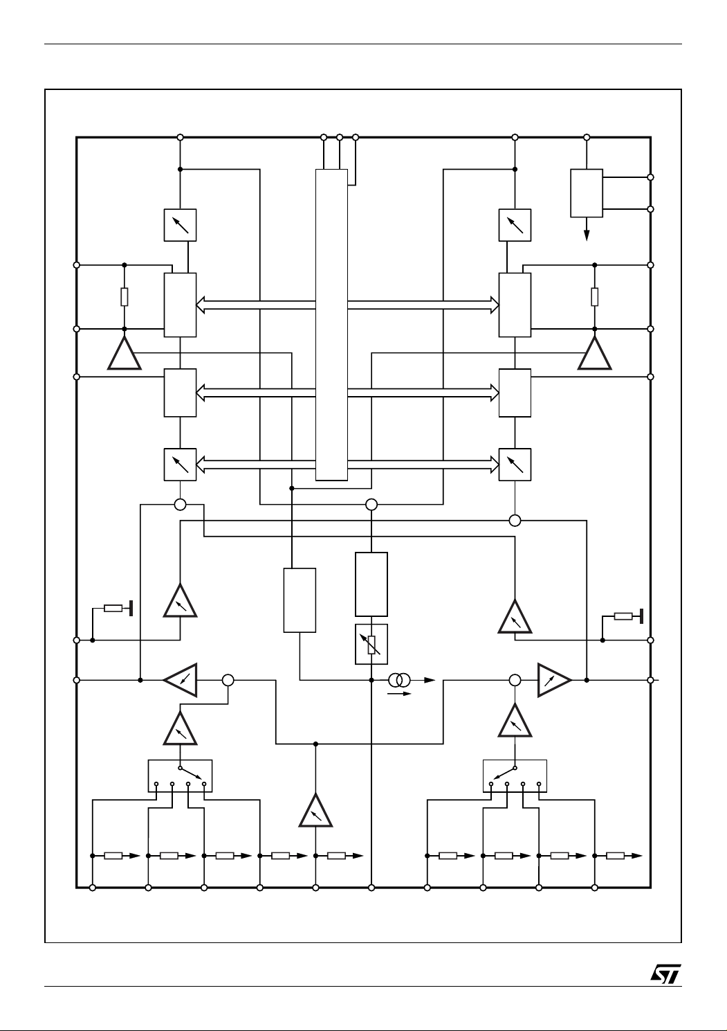
Figure 2. PIN CONNECTION (Top view)
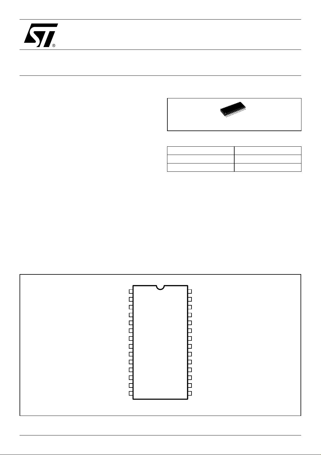
gure 1. Package
SO28
Table 1. Order Codes
Part Number Package
TDA7468D SO28
TDA7468D13TR Tape & Reel
applications in Hi-Fi systems.
Selectable input gain is provided. Control of all the
functions is accomplished by serial bus.
The AC signal setting is obtained by resistor networks and switches combined with operational
amplifiers.
Thanks to the used BIPOLAR/CMOS Technology,
Low Distortion, Low Noise and DC stepping are
obtained
April 2010
V
1
S
MIC
IN1_L
IN2_L
IN3_L IN3_R
IN4_L
MUX_L
IS_L
TREBLE_L
BASSI_L
BASSO_L
OUT_L
DGND
SCL
2
3
4
5
6
7
8
9
10
11
12
13
14
D99AU1057
28
27
26
25
24
22
21
20
19
18
17
16
15
GND
CREF
IN1_R
IN2_R
IN4_R23
MUX_R
IS_R
TREBLE_R
BASSI_R
BASSO_R
OUT_R
ALC
SDA
Rev. 4
1/23
TDA7468
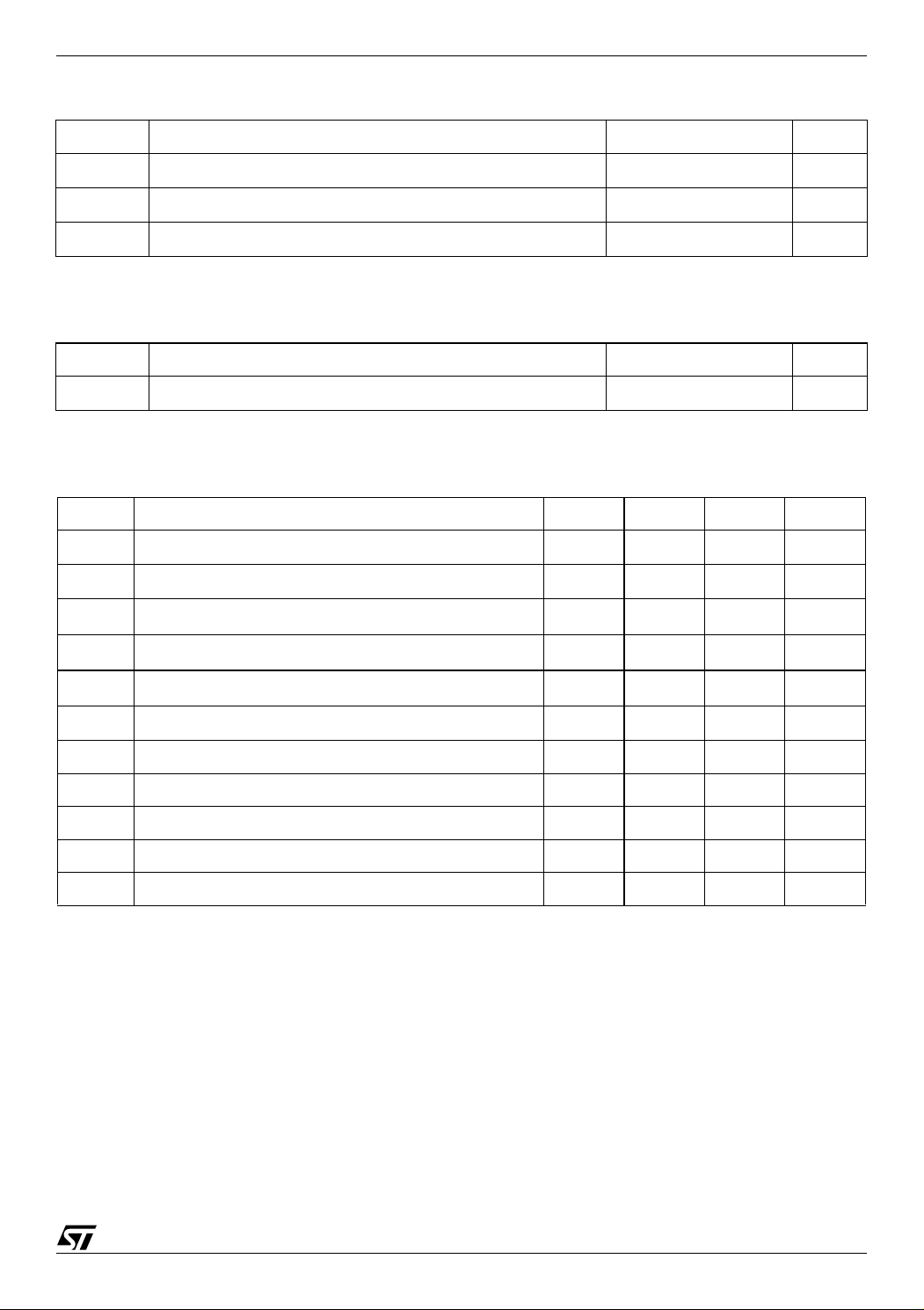
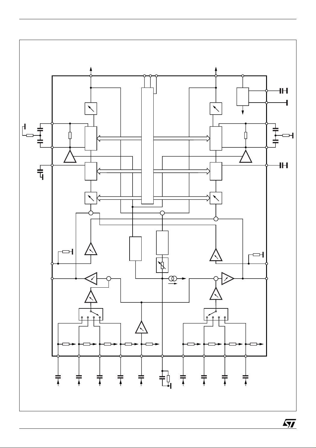
Figure 3. BLOCK DIAGRAM
18
BASSO-R
192021
BASSI-R
TREBLE-R
gm
63dB att.
OUT-R
17
-24 att.
/8dB step
BASS
/2dB step
-14 to +14dB
TREBLE
/2dB step
-14 to +14dB
/1dB step
+ 6dB gain
+
DGND
SCL
SDA
131215
14
C BUS DECODER + LATCHES
2
I
+
OUT-L
-24 att.
BASS
-14 to +14dB
TREBLE
-14 to +14dB
63dB att.
+
/8dB step
/2dB step
/2dB step
/1dB step
+ 6dB gain
S
1
SUPPLY V
REF
V
gm
GND CREFTREBLE-LMUX-L IS-L
BASSO-LBASSI-L
IS-R
22
MUX-R
23
IN-R4
50K
50K
inverting
non-inverting
/ 2dB step
buffer gain:
0 to 14dB gain
INPUT
SELECT
24
IN-R3
50K
MIX
VARIABLE
0dB
6dB
9dB
12dB
25
IN-R2
+
50K
26
IN-R1
BASS_ALC
50K
CONTROL
0dB, 6dB
10dB, 14dB
2
50K
MIC-MIX
RECTIFIER
HALF_WAVE
16
ALC
3
IN-L1
INPUT
50K
inverting
non-inverting
/ 2dB step
buffer gain:
0 to 14dB gain
SELECT
50K
4
IN-L2
VARIABLE
0dB
+
5
MIX
6dB
IN-L3
9dB
12dB
50K
6
50K
78 9 10 11 2827
50K
D99AU1058A
IN-L4
2/23
TDA7468
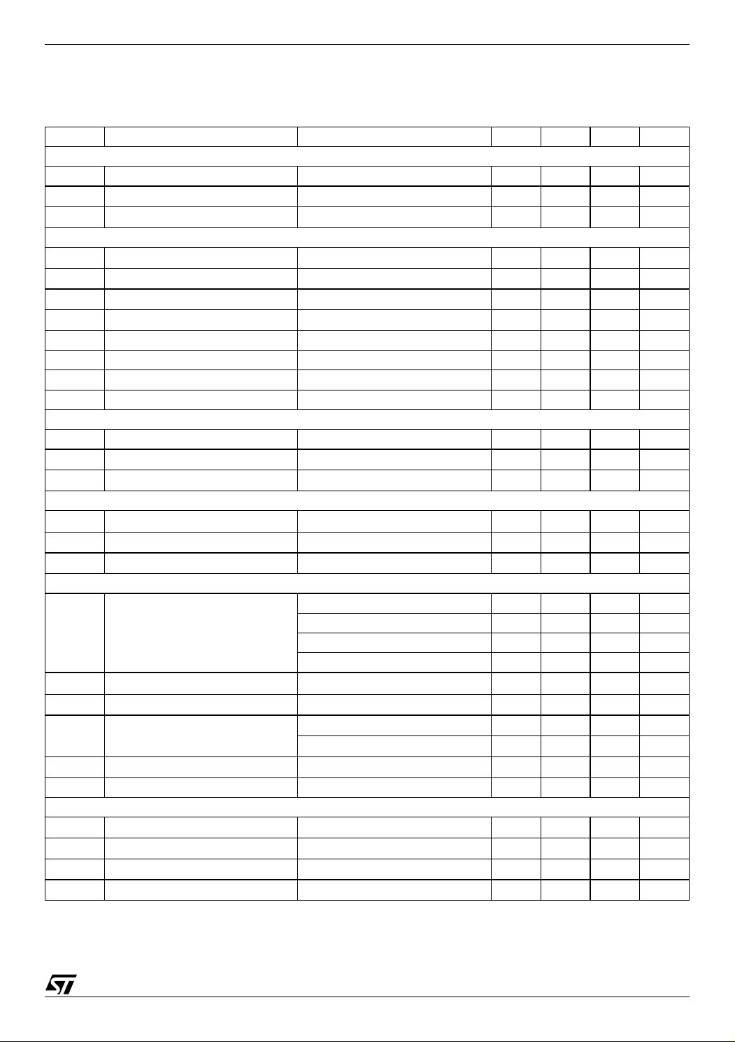
Table 2. ABSOLUTE MAXIMUM RATINGS
Symbol Parameter Value Unit
T
T
V
amb
stg
Operating Supply Voltage 10.5 V
S
Operating Ambient Temperature 0 to 70 °C
Storage Temperature Range -55 to 150 °C
Table 3. THERMAL DATA
Symbol Parameter Value Unit
R
th j-pin
Thermal Resistance Junction-pins 85 °C/W
Table 4. QUICK REFERENCE DATA
Symbol Parameter Min. Typ. Max. Unit
V
V
THD
Supply Voltage 5 9 10 V
S
Max. input signal handling 2 Vrms
CL
Total Harmonic Distortion V
Total Harmonic Distortion V
= 1Vrms; f = 1KHz
I
= 0.1Vrms; f = 1KHz
I
0.01 % %
0.1 %
S/N
S
Signal to Noise Ratio V
Channel Separation f = 1KHz 90 dB
C
= 1Vrms (0dB)
out
100 dB
Input Gain (2dB step) 0 14 dB
Volume Control (1dB step) -87 0 dB
Treble Control (2dB step) -14 +14 dB
Bass Control (2dB step) -14 +14 dB
Mute Attenuation 86 dB
3/23
TDA7468
ELECTRICAL CHARACTERISTICS
(refer to the test circuit T
specified)
Symbol Parameter Test Condition Min. Typ. Max. Unit
SUPPLY
V
SVR Ripple Rejection 60 90 dB
INPUT STAGE
R
V
S
G
inmin
G
inmax
G
MIC
R
G
G
G
G
MIX
SURROUND
R
G
inmin
G
inmax
G
M
M
ixmax
CrosstalkCrosstalk of Mux Output to 100%
G
buffer
VOLUME CONTROL
C
RANGE1
A
VMAX1
A
STEP1
Match1 Matching TBD dB
C
RANGE2
A
VMAX2
A
STEP2
Match2 Matching TBD dB
A
VMAX1
A
VMAX2
Supply Voltage 5 9 10 V
S
Supply Current 9 mA
I
S
Input Resistance 35 50 65 KΩ
IN
Clipping Level THD = 0.3% 2 2.5
CL
Input Separation 80 100 dB
IN
Minimum Input Gain -1 0 1 dB
Maximum Input Gain 14 dB
Step Resolution 2 dB
step
Input Resistance 35 50 65 KΩ
IN
Mic Input Gain 1 14 dB
mic1
Mic Input Gain 2 10 dB
mic2
Mic Input Gain 3 6 dB
mic3
Mic Input Gain 4 0 dB
min4
Mixing Rate 50 %
mic
Input Resistance 35 50 65 KΩ
in
Minimum Input Gain -1 0 1 dB
Maximum Input Gain 12 dB
Inverting Gain -1
inV
Minimum Mixing Rate 0 %
ixmin
Maximum Mixing Rate 100 %
IS
Buffer Gain 6dB
Vol 1 Control Range 63 dB
Vol 1 Max. Attenuation 61 63 65 dB
Vol 1 Step Resolution 0.5 1 1.5 dB
Vol 2 Control Range 24 dB
Vol 2 Max. Attenuation 22 24 26 dB
Vol 2 Step Resolution 7 8 9 dB
+
Vol 1 + Vol 2 Max Attenuation 84 dB
= 25°C, VS = 9V, f = 1KHz all controls flat (G = 0dB), unless otherwise
amb
40 dB
Vrms
4/23
TDA7468
ELECTRICAL CHARACTERISTICS (continua)
(refer to the test circuit T
specified)
Symbol Parameter Test Condition Min. Typ. Max. Unit
BASS CONTROL
Gb Control Range Max. Boost/cut ±12.0 ±14.0 ±16.0 dB
B
STEP
R
BASS ALC CONTROL
R
attack1
R
attack2
R
attack3
R
attack4
Thresh1 Threshold 1 700 mVrms
Thresh2 Threshold 2 485 mVrms
Thresh3 Threshold 3 320 mVrms
Thresh4 Threshold 4 170 mVrms
TREBLE CONTROL
Gt Control Range Max. Boost/cut +13.0 +14.0 +15.0 dB
T
STEP
AUDIO OUTPUTS
V
R
VO
GENERAL
E
S/N Signal to Noise Ratio
S
S
BUS INPUT
V
V
I
V
Step Resolution 1 2 3 dB
Internal Feedback Resistance 33 44 55 KΩ
B
Attack Time Resistor 1 12.5 KΩ
Attack Time Resistor 2 25 KΩ
Attack Time Resistor 3 50 KΩ
Attack Time Resistor 4 100 KΩ
Step Resolution 1 2 3 dB
R
Internal Resistance 25 KΩ
t
Clipping Level THD = 0.3% 2 2.5
OCL
Output Load Resistance 2 KΩ
L
DC Voltage Level 4.5 V
UT
Output Noise BW = 20Hz to 20KHz;
NO
Channel Separation Left/Right 90 dB
C
dDistortion A
Channel Separation left/right 90 dB
C
Total Tracking Error 0 1 dB
Input Low Voltage 1V
IL
Input High Voltage 2.5 V
IH
Input Current VIN = 0.4V -5 5 µA
IN
Output Voltage (ACK) IO = 1.6mA 0.4 0.8 V
O
= 25°C, VS = 9V, f = 1KHz all controls flat (G = 0dB), unless otherwise
amb
All gains 0dB;
output muted 5 µV
flat 10 15 µV
All gains 0dB
= 0; VI = 0.1V
V
A
= 0; VI = 1V
V
; V
O
rms
= 1V
rms
;
rms
; 0.1 %
; 0.01 %
100 dB
Vrms
5/23
TDA7468
Figure 4. TEST CIRCUIT
-24 att.
BASSO-R
18192021
5.6K
100nF 100nF
BASSI-R
-14 to +14dB
OUT-R
17
/8dB step
BASS
/2dB step
S
-24 att.
/8dB step
/2dB step
-14 to +14dB
V
1
SUPPLY
10µF
REF
V
GND CREFTREBLE-L
BASSO-LBASSI-L
DGND
SCL
SDA
131215
14
OUT-L
BASS
3.3nF
TREBLE-R
IS-R
22
MUX-R
50K
gm
63dB att.
buffer gain:
INPUT
SELECT
TREBLE
/2dB step
-14 to +14dB
/1dB step
+ 6dB gain
+
MIX
VARIABLE
inverting
non-inverting
/ 2dB step
0 to 14dB gain
0dB
6dB
9dB
12dB
+
C BUS DECODER + LATCHES
2
I
+
0dB, 6dB
10dB, 14dB
HALF_WAVE
CONTROL
BASS_ALC
RECTIFIER
inverting
non-inverting
/ 2dB step
buffer gain:
0 to 14dB gain
INPUT
SELECT
TREBLE
+
VARIABLE
0dB
+
/2dB step
-14 to +14dB
63dB att.
/1dB step
+ 6dB gain
MIX
6dB
9dB
12dB
gm
50K
78 9 10 11 2827
MUX-L IS-L
6/23
0.47µF
23
IN-R4
50K
0.47µF
24
IN-R3
50K
0.47µF
25
IN-R2
50K
0.47µF
26
IN-R1
50K
2
MIC-MIX
0.47µF
50K
50K
16
ALC
0.47µF
3
IN-L1
1M
0.47µF
50K
4
IN-L2
0.47µF
0.47µF
5
IN-L3
50K
0.47µF
6
IN-L4
50K
D99AU1059A
TDA7468
3 APPLICATION SUGGESTIONS
The first and the last stages are volume control blocks. The control range is 0 to -63dB (mute) with 1dB
step resolution for this first one, 0 to 24dB (mute) with 8dB step resolution for the last one.
The very high resolution allows the implementation of systems free from any noisy acoustical effect.
The TDA7468D audioprocessor provides 2 bands tones control.
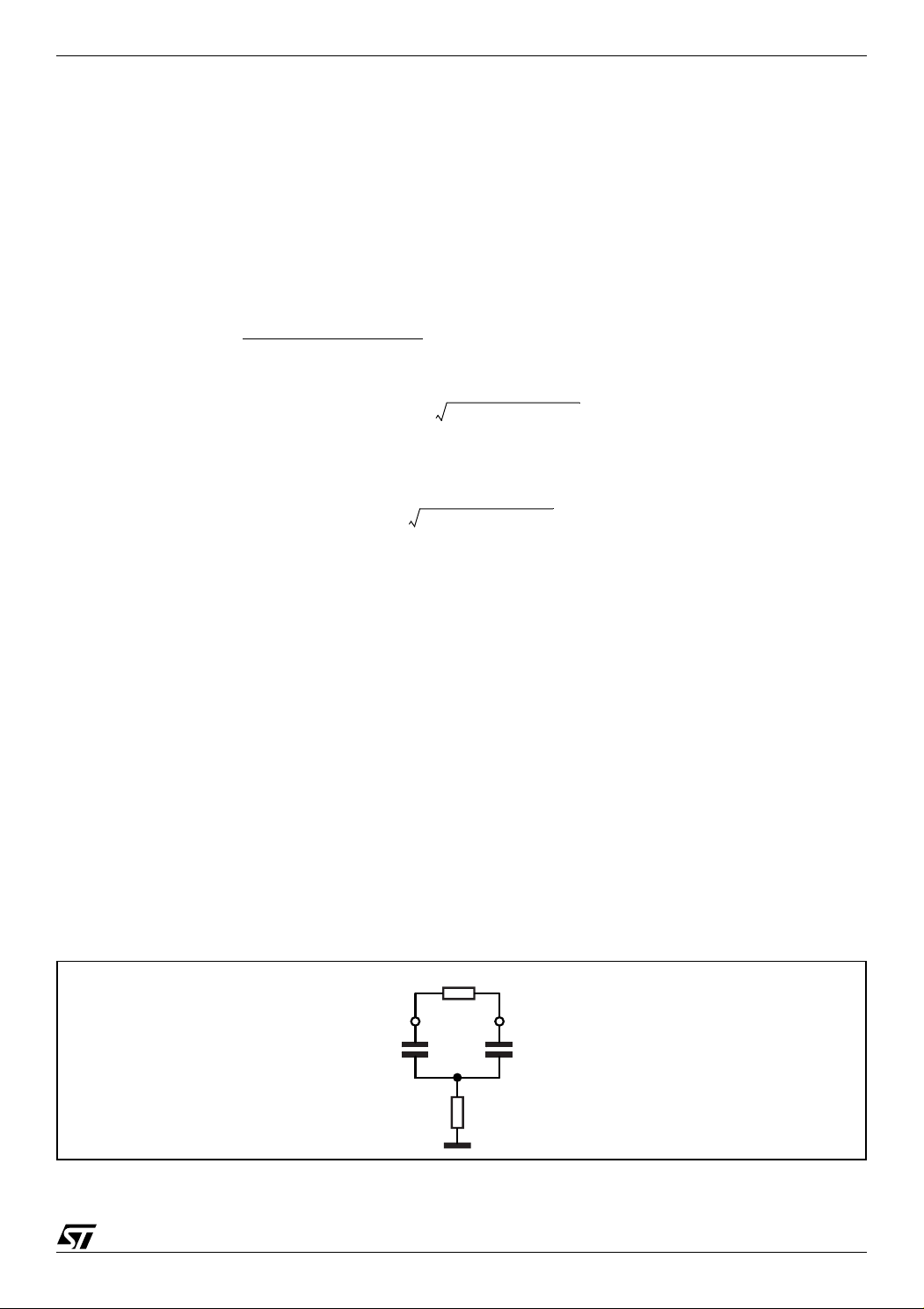
3.1 Bass, Stages
The Bass cell has an internal resistor R
Several filter types can be implemented, connecting external components to the Bass IN and OUT pins.
The fig.5 refers to basic T Type Bandpass Filter
R2,C1,C2 external) the centre frequency Fc, the gain Av at max. boost and the filter Q factor are computed
as follows:
= 44KΩ typical.
i
F
-----------------------------------------------------------------=
C
2 π R1 R2 C1 C2⋅⋅⋅⋅⋅
R2 C2 R2 C1 Ri C1++
A
----------------------------------------------------------------=
V
starting from the filter component values (R1 internal and
1
R2 C1 R2 C2+
R1 R2 C1 C2⋅⋅⋅
------------------------------------------------- -=
R2 C1 R2 C2+
1–
V
CRi
Q⋅⋅ ⋅ ⋅
---------------------------------------------------------------------- -=
2 π C1 F
C2
1– Q2–
A
V
CAV
2
C1⋅
Q
----------------------------- -==
1– Q2–
A
V
1–()Q⋅⋅ ⋅⋅⋅
Viceversa, once F
Q
, AV, and Ri internal value are fixed, the external components values will be:
C
A
----------------------------------------- -
C1
2 π F
R2
3.2 Treble Stage
The treble stage is a high pass filter whose time constant is fixed by an internal resistor (25KΩ typical) and
an external capacitor connected between treble pins and ground.
3.3 CREF
The suggested 10µF reference capacitor (CREF) value can be reduced to 4.7µF if the application requires
faster power ON.
Figure 5.
Ri internal
OUTIN
C
1
C
2
R
2
D95AU313
7/23

TDA7468
4I2C BUS INTERFACE
Data transmission from microprocessor to the TDA7468D and vice versa takes place through the 2 wires
2
I
C BUS interface, consisting of the two lines SDA and SCL (pull-up resistors to positive supply voltage
must be connected).
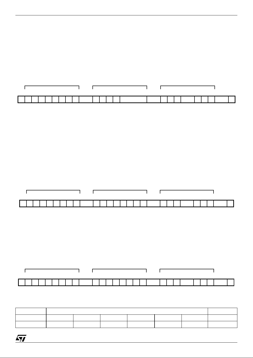
4.1 Data Validity
As shown in fig. 6, the data on the SDA line must be stable during the high period of the clock. The HIGH
and LOW state of the data line can only change when the clock signal on the SCL line is LOW.
4.2 Start and Stop Conditions
As shown in fig.7 a start condition is a HIGH to LOW transition of the SDA line while SCL is HIGH. The
stop condition is a LOW to HIGH transition of the SDA line while SCL is HIGH.
4.3 Byte Format
Every byte transferred on the SDA line must contain 8 bits. Each byte must be followed by an acknowledge
bit. The MSB is transferred first.
4.4 Acknowledge
The master (µP) puts a restive HIGH level on the SDA line during the acknowledge clock pulse (see fig.
4). The peripheral (audio processor) that acknowledges has to pull-down (LOW) the SDA line during this
clock pulse. The audio processor which has been addressed has to generate an acknowledge after the
reception of each byte, otherwise the SDA line remains at the HIGH level during the ninth clock pulse time.
In this case the master transmitter can generate the STOP information in order to abort the transfer.
4.5 Transmission without Acknowledge
Avoiding to detect the acknowledge of the audio processor, the µP can use a simpler transmission: simply
it waits one clock without checking the slave acknowledging, and sends the new data. This approach of
course is less protected from misworking.
SCL
SDA
SDA
SCL
START
2
CBUS
2
CBUS
START
2
CBUS
DATA LINE
STABLE, DATA
VALID
1
MSB
CHANGE
DATA
ALLOWED
D99AU1032
23789
D99AU1033
D99AU1031
2
I
CBUS
STOP
ACKNOWLEDGMENT
FROM RECEIVER
Figure 6. Data Validity on the I
Figure 7. Timing Diagram of I
Figure 8. Acknowledge on the I
SCL
SDA
8/23
5 SOFTWARE SPECIFICATION
Interface Protocol
The interface protocol comprises:
A start condition (S)
A chip address byte, containing the TDA7468D address
A subaddress bytes
A sequence of data (N byte + acknowledge)
A stop condition (P)
CHIP ADDRESS
SUBADDRESS DATA 1 to DATA n
TDA7468
MSB
S 1 0 0 0 1 0 0 0 ACK ACK DATA ACK P
D96AU420
LSB MSB LSB MSB LSB
X
X
X
DATA
B
ACK = Acknowledge
S = Start; P = Stop
A = Address
B = Auto Increment
6 EXAMPLES
6.1 No Incremental Bus
The TDA7468D receives a start condition, the correct chip address, a subaddress with the B = 0 (no incremental bus), N-data (all these data concern the subaddress selected), a stop condition.
CHIP ADDRESS
MSB
S 1 0 0 0 1 0 0 0 ACK ACK DATA ACK P
D96AU421
LSB MSB LSB MSB LSB
6.2 Incremental Bus
The TDA7468D receive a start conditions, the correct chip address, a subaddress with the B = 1 (incremental bus): now it is in a loop condition with an autoincrease of the subaddress whereas SUBADDRESS
from "XXX1000" to "XXX1111" of DATA are ignored.
The DATA 1 concern the subaddress sent, and the DATA 2 concern the subaddress sent plus one in the
loop etc, and at the end it receivers the stop condition.
SUBADDRESS DATA
0
X
D3
X
X
D2 D1 D0
CHIP ADDRESS
MSB
S 1 0 0 0 1 0 0 0 ACK ACK DATA ACK P
D96AU422
LSB MSB LSB MSB LSB
SUBADDRESS DATA 1 to DATA n
1
X
X
X
D3
D2 D1 D0
Table 5. POWER ON RESET CONDITION
MSB LSB
D7 D6 D5 D4 D3 D2 D1 D0
1 111111 0
9/23

TDA7468
7 DATA BYTES
Address = (HEX) 10001000.
Table 6. FUNCTION SELECTION: First byte (subaddress)
MSB LSB
D7 D6 D5 D4 D3 D2 D1 D0
X X X B 0 0 0 0 INPUT SELECT & MIC
XXXB0 0 01INPUT GAIN
X X X B 0 0 1 0 SURROUND
XXXB0 0 11VOLUME LEFT
XXXB0 1 00VOLUME RIGHT
X X X B 0 1 0 1 TREBLE & BASS
XXXB0 1 10OUTPUT
X X X B 0 1 1 1 BASS ALC
B = 1: INCREMENTAL BUS; ACTIVE
B = 0: NO INCREMENTAL BUS
X = INDIFFERENT 0/1
SUBADDRESS
Table 7. INPUT SELECTION & MIC
MSB LSB
D7 D6 D5 D4 D3 D2 D1 D0
INPUT SELECT
000 IN1
001 IN2
010 IN3
011 IN4
MUTE (IN5)
1 ON (IN5)
0OFF
0 0 Gain: 14dB
0 1 Gain: 10dB
1 0 Gain: 6dB
1 1 Gain: 0dB
1 OFF
0 ON
MIC
10/23

Table 8. INPUT GAIN SELECTION
MSB LSB INPUT GAIN
D7 D6 D5 D4 D3 D2 D1 D0 2dB STEPS
0 0 0 0dB
0 0 1 2dB
0 1 0 4dB
0 1 1 6dB
1 0 0 8dB
1 0 1 10dB
1 1 0 12dB
1 1 1 14dB
GAIN = 0 to 30dB
Table 9. SURROUND
MSB LSB SURROUND
D7 D6 D5 D4 D3 D2 D1 D0
SURROUND MODE
1ON
TDA7468
0OFF
GAIN
00 0dB
01 6dB
10 9dB
1 1 12dB
MIXING
0 0 0 inverting : 100%
0 0 1 inverting :50%
0 1 0 inverting : 25%
011 0%
1 0 0 non-inverting : 100%
1 0 1 non-inverting : 75%
1 1 0 non-inverting : 50%
111 mute
BUFFER GAIN
10
06dB
11/23

TDA7468
Table 10. VOLUME
MSB LSB VOLUME
D7 D6 D5 D4 D3 D2 D1 D0 1dB STEPS
0 0 0 0dB
0 0 1 -1dB
0 1 0 -2dB
0 1 1 -3dB
1 0 0 -4dB
1 0 1 -5dB
1 1 0 -6dB
1 1 1 -7dB
8dB STEPS
0 0 0 0dB
0 0 1 -8dB
0 1 0 -16dB
0 1 1 -24dB
1 0 0 -32dB
1 0 1 -40dB
1 1 0 -48dB
1 1 1 -56dB
VOLUME 2
00 0dB
01 -8dB
10 -16dB
11 -24dB
VOLUME = 0 to-87dB
Table 11. VOLUME setting 1
Target Volume (dB) Volume1 1dB step (dB) Volume1 8dB step (dB) Volume2 8dB step (dB)
0000
-1 -1
-2 -2
-3 -3
-4 -4
-5 -5
-6 -6
-7 -7
-80-80
-9 -1
-10 -2
-11 -3
-12 -4
-13 -5
-14 -6
-15 -7
12/23

Table 11. VOLUME setting 1 (continua)
Target Volume (dB) Volume1 1dB step (dB) Volume1 8dB step (dB) Volume2 8dB step (dB)
-160-160
-17 -1
-18 -2
-19 -3
-20 -4
-21 -5
-22 -6
-23 -7
-240-240
-25 -1
-26 -2
-27 -3
-28 -4
-29 -5
-30 -6
-31 -7
-320-320
-33 -1
-34 -2
-35 -3
-36 -4
-37 -5
-38 -6
-39 -7
-400-400
-41 -1
-42 -2
-43 -3
-44 -4
-45 -5
-46 -6
-47 -7
-480-480
-49 -1
-50 -2
-51 -3
-52 -4
-53 -5
-54 -6
-55 -7
Target Volume (dB) Volume1 1dB step (dB) Volume1 8dB step (dB) Volume2 8dB step (dB)
-560-560
-57 -1
TDA7468
13/23

TDA7468
Table 11. VOLUME setting 1 (continua)
-58 -2
-59 -3
-60 -4
-61 -5
-62 -6
-63 -7
-640-568
-65 -1
-66 -2
-67 -3
-68 -4
-69 -5
-70 -6
-71 -7
-72 0 -56 -16
-73 -1
-74 -2
-75 -3
-76 -4
-77 -5
-78 -6
-79 -7
-80 0 -56 -24
-81 -1
-82 -2
-83 -3
-84 -4
-85 -5
-86 -6
-87 -7
Table 12. VOLUME setting 2
Target Volume (dB) Volume1 1dB step (dB) Volume1 8dB step (dB) Volume2 8dB step (dB)
0000
-1 -1
-2 -2
-3 -3
-4 -4
-5 -5
-6 -6
-7 -7
14/23

Table 12. VOLUME setting 2 (continua)
Target Volume (dB) Volume1 1dB step (dB) Volume1 8dB step (dB) Volume2 8dB step (dB)
-80-80
-9 -1
-10 -2
-11 -3
-12 -4
-13 -5
-14 -6
-15 -7
-160-160
-17 -1
-18 -2
-19 -3
-20 -4
-21 -5
-22 -6
-23 -7
-240-16-8
-25 -1
-26 -2
-27 -3
-28 -4
-29 -5
-30 -6
-31 -7
-32 0 -16 -16
-33 -1
-34 -2
-35 -3
-36 -4
-37 -5
-38 -6
-39 -7
-40 0 -16 -24
-41 -1
-42 -2
-43 -3
-44 -4
-45 -5
-46 -6
-47 -7
TDA7468
15/23
TDA7468
Table 12. VOLUME setting 2 (continua)
Target Volume (dB) Volume1 1dB step (dB) Volume1 8dB step (dB) Volume2 8dB step (dB)
-48 0 -24 -24
-49 -1
-50 -2
-51 -3
-52 -4
-53 -5
-54 -6
-55 -7
-56 0 -32 -24
-57 -1
-58 -2
-59 -3
-60 -4
-61 -5
-62 -6
-63 -7
-64 0 -40 -24
-65 -1
-66 -2
-67 -3
-68 -4
-69 -5
-70 -6
-71 -7
-72 0 -48 -24
-73 -1
-74 -2
-75 -3
-76 -4
-77 -5
-78 -6
-79 -7
-80 0 -56 -24
-81 -1
-82 -2
-83 -3
-84 -4
-85 -5
-86 -6
-87 -7
16/23
Table 13. TREBLE & BASS SELECTION
MSB LSB
D7 D6 D5 D4 D3 D2 D1 D0 TREBLE
0 0 0 0 -14dB
0 0 0 1 -12dB
0 0 1 0 -10dB
0011 -8dB
0100 -6dB
0101 -4dB
0110 -2dB
0111 0dB
1 0 0 0 14dB
1 0 0 1 12dB
1 0 1 0 10dB
1011 8dB
1100 6dB
1101 4dB
1110 2dB
1111 0dB
BASS (*)
0 0 0 0 -14dB
0 0 0 1 -12dB
0 0 1 0 -10dB
0011 -8dB
0100 -6dB
0101 -4dB
0110 -2dB
0111 0dB
1 0 0 0 14dB
1 0 0 1 12dB
1 0 1 0 10dB
1011 8dB
1100 6dB
1101 4dB
1110 2dB
1111 0dB
TDA7468
(*) When BASS is programmed in the range -14dB/0dB, ALC is automatically switched to "OFF".
Table 14. OUTPUT
MSB LSB
D7 D6 D5 D4 D3 D2 D1 D0 MUTE
0ON
1OFF
17/23
TDA7468
A
Table 15. BASS ALC
MSB LSB BASS ALC
D7 D6 D5 D4 D3 D2 D1 D0
ALC Mode
1ON
0OFF
Detector
1ON
0OFF
Release Current Circuit
1ON
0OFF
Attack Time Resistor
0 0 12.5KΩ
0 1 25KΩ
1 0 50KΩ
1 1 100KΩ
Threshold
0 0 700mVrms
0 1 485mVrms
1 0 320mVrms
1 1 170mVrms
Attack Mode
0 MODE 1: Fixed Resistor
1 MODE 2: Adaptive
Figure 9. BASS ALC : Threshold curve Figure 10. BASS ALC : THD
V
O
(V
RMS
1
0.1
18/23
)
Supply Voltage : 9.0V
Frequency : 60Hz
Bassfilter : 60Hz/28dB boost
Internal release circuit : ON
Attack mode : 12.5kohm, mode2(adaptive)
0.01 0.1 1
Threshold3
Threshold4
D00AU1100
Threshold1
Threshold2
VIN(VRMS)
THD
[%]
Supply Voltage : 9.0V
Frequency : 60Hz
10
Bassfilter : 60Hz/28dB boost
Internal release circuit : ON
Attack mode : 12.5kohm, mode2(adaptive)
1
0.1
0.01
0.001
Threshold4
Threshold3
Threshold1
Threshold2
0.01 0.1 1VIN(V
D99AU1101
RMS
)
8IC1
4
6
7
TDA7468
Figure 11. PINS: IN1_L, IN1_R, IN2_L, IN2_R,
IN3_L, IN3_R, IN4_L, IN4 _R, IS_L,
IS_R, MIC
V
S
20µA
50K
GND
Vref
D99AU1092
Figure 12. PINS: OUT_L, OUT_R, IMUX_L,
MUX_R
V
S
20µA
10Ω
GND
D99AU1093
Figure 15. PINS: BASSI_L, BASSI_R
V
S
20µA
GND
BASSO-L,BASSO-R
45K
D99AU109
Figure 16. PINS: BASSO_L, BASSO_R
V
S
20µA
45K
GND
BASSI-L,BASSI-R
D99AU109
Figure 17. PIN: ALC
Figure 13. PINS: TREBLE_L, TREBLE_R
V
S
20µA
25K
GND
D99AU109
Figure 14. PINS: SCL, SDA
V
S
20µA
GND
D99AU1095
V
S
GND
Figure 18. PIN: CREF
V
S
GND
20µA
100K
D99AU1098
20µA
25K
25K
D99AU1099
19/23

TDA7468
9 PACKAGE MECHANICAL DATA
In order to meet environmental requirements, ST offers these devices in different grades of ECOPACK
packages, depending on their level of environmental compliance. ECOPACK® specifications, grade definitions and product status are available at: www.st.com. ECOPACK
®
is an ST trademark.
®
20/23
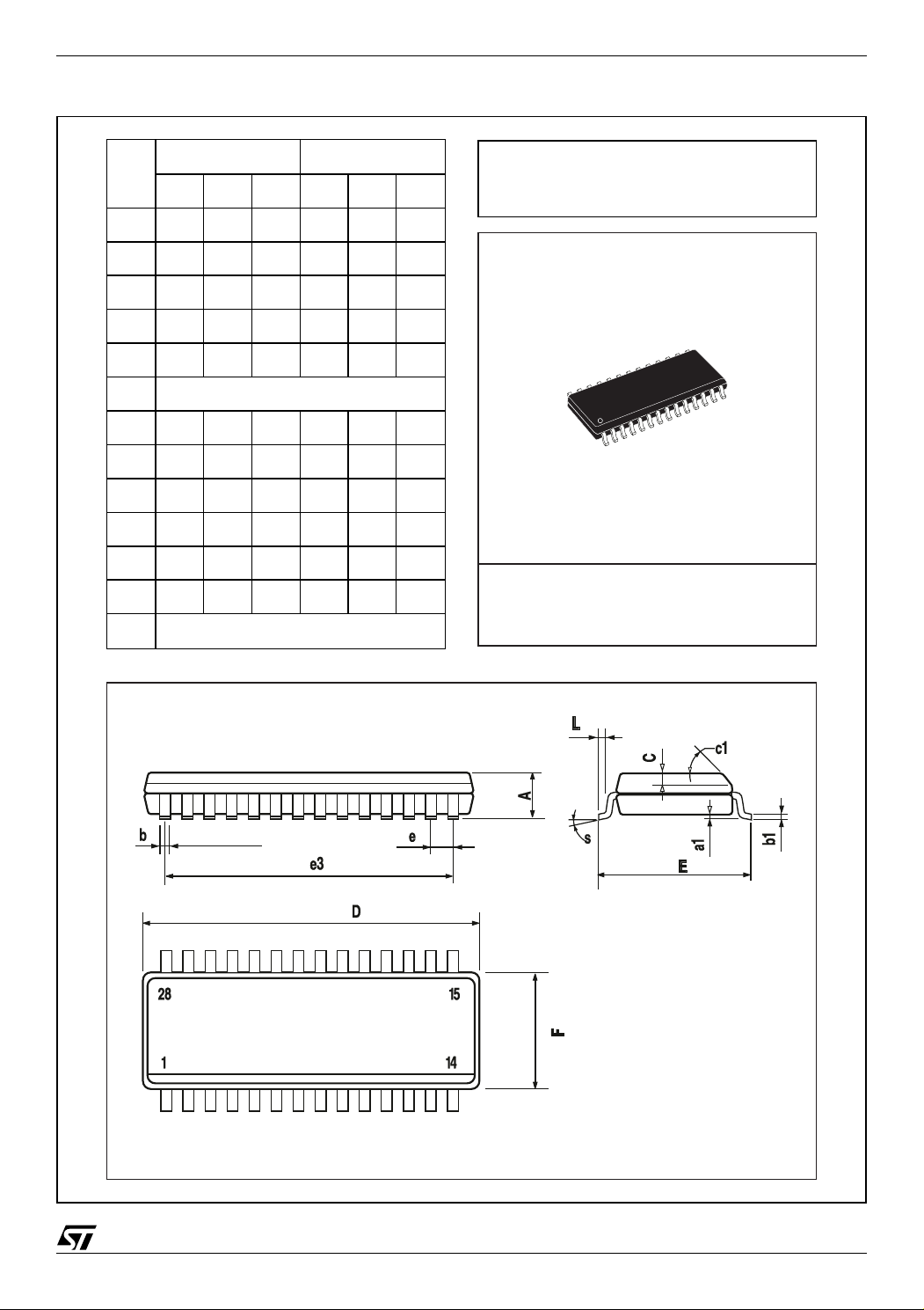
Figure 19. SO28 Mechanical Data & Package Dimensions
TDA7468
DIM.
A 2.65 0.104
a1 0.1 0.3 0.004 0.012
b 0.35 0.49 0.014 0.019
b1 0.23 0.32 0.009 0.013
C 0.5 0.020
c1 45° (typ.)
D 17.7 18.1 0.697 0.713
E 10 10.65 0.394 0.419
e 1.27 0.050
e3 16.51 0.65
F 7.4 7.6 0.291 0.299
L 0.4 1.27 0.016 0.050
S8
mm inch
MIN. TYP. MAX. MIN. TYP. MAX.
(max.)
°
OUTLINE AND
MECHANICAL DATA
SO-28
21/23

TDA7468
10 REVISION HISTORY
Table 16. Revision History
Date Revision Description of Changes
January 2004 1 First Issue in EDOCS DMS
June 2004 2 Changed the Style-sheet in compliance to the new “Corporate Technical
March 2006 3 Updated figure 19 “SO28 Mechanical Data & Package Dimensions”
30-Apr-2010 4 Updated title and added environmental compliance statement for
Pubblications Design Guide”
package
22/23

TDA7468
Please Read Carefully:
Information in this document is provided solely in connection with ST products. STMicroelectronics NV and its subsidiaries (“ST”) reserve the
right to make changes, corrections, modifications or improvements, to this document, and the products and services described herein at any
time, without notice.
All ST products are sold pursuant to ST’s terms and conditions of sale.
Purchasers are solely responsible for the choice, selection and use of the ST products and services described herein, and ST assumes no
liability whatsoever relating to the choice, selection or use of the ST products and services described herein.
No license, express or implied, by estoppel or otherwise, to any intellectual property rights is granted under this document. If any part of this
document refers to any third party products or services it shall not be deemed a license grant by ST for the use of such third party products
or services, or any intellectual property contained therein or considered as a warranty covering the use in any manner whatsoever of such
third party products or services or any intellectual property contained therein.
UNLESS OTHERWISE SET FORTH IN ST’S TERMS AND CONDITIONS OF SALE ST DISCLAIMS ANY EXPRESS OR IMPLIED
WARRANTY WITH RESPECT TO THE USE AND/OR SALE OF ST PRODUCTS INCLUDING WITHOUT LIMITATION IMPLIED
WARRANTIES OF MERCHANTABILITY, FITNESS FOR A PARTICULAR PURPOSE (AND THEIR EQUIVALENTS UNDER THE LAWS
OF ANY JURISDICTION), OR INFRINGEMENT OF ANY PATENT, COPYRIGHT OR OTHER INTELLECTUAL PROPERTY RIGHT.
UNLESS EXPRESSLY APPROVED IN WRITING BY AN AUTHORIZED ST REPRESENTATIVE, ST PRODUCTS ARE NOT
RECOMMENDED, AUTHORIZED OR WARRANTED FOR USE IN MILITARY, AIR CRAFT, SPACE, LIFE SAVING, OR LIFE
SUSTAINING APPLICATIONS, NOR IN PRODUCTS OR SYSTEMS WHERE FAILURE OR MALFUNCTION MAY RESULT IN
PERSONAL INJURY, DEATH, OR SEVERE PROPERTY OR ENVIRONMENTAL DAMAGE. ST PRODUCTS WHICH ARE NOT
SPECIFIED AS "AUTOMOTIVE GRADE" MAY ONLY BE USED IN AUTOMOTIVE APPLICATIONS AT USER’S OWN RISK.
Resale of ST products with provisions different from the statements and/or technical features set forth in this document shall immediately void
any warranty granted by ST for the ST product or service described herein and shall not create or extend in any manner whatsoever, any
liability of ST.
ST and the ST logo are trademarks or registered trademarks of ST in various countries.
Information in this document supersedes and replaces all information previously supplied.
The ST logo is a registered trademark of STMicroelectronics. All other names are the property of their respective owners.
© 2010 STMicroelectronics - All rights reserved
STMicroelectronics group of companies
Australia - Belgium - Brazil - Canada - China - Czech Republic - Finland - France - Germany - Hong Kong - India - Israel - Italy - Japan -
Malaysia - Malta - Morocco - Philippines - Singapore - Spain - Sweden - Switzerland - United Kingdom - United States of America
www.st.com
23/23
 Loading...