

Three-band digitally-controlled audio processor
Features
! Input multiplexer
– four stereo inputs
– selectable input gain for optimal adaptation
to different sources
! Single stereo output
! Treble, mid-range and bass control in 2-dB
steps
! Volume control in 1-dB steps
! Two speaker attenuators:
– two independent speaker controls in 1-dB
steps for balance facility
– independent mute function
! All functions are programmable via serial bus.
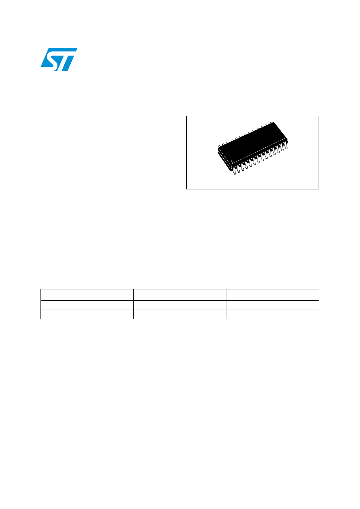
TDA7439DS
SO28
processor for quality audio applications in
car-radio and Hi-Fi systems. Selectable input gain
is provided. All the functions are controlled by
serial bus.
The AC signal setting is obtained by resistor
networks and switches combined with operational
amplifiers.
Description
The TDA7439DS is a volume, tone (bass,
mid-range and treble) and balance (left/right)
Table 1. Device summary
Order codes Package Packaging
TDA7439DS SO28 Tube
TDA7439DS
13TR SO28 Tape and Reel
The TDA7439DS employs BIPOLAR/CMOS
technology to provide low distortion, low noise
and DC stepping.
November 2007 Rev 4 1/23
www.st.com
23

Contents TDA7439DS
Contents
1 Block diagram and pin out . . . . . . . . . . . . . . . . . . . . . . . . . . . . . . . . . . . . 3
2 Electrical specifications . . . . . . . . . . . . . . . . . . . . . . . . . . . . . . . . . . . . . . 4
3 Application suggestions . . . . . . . . . . . . . . . . . . . . . . . . . . . . . . . . . . . . . . 8
3.1 Tone control . . . . . . . . . . . . . . . . . . . . . . . . . . . . . . . . . . . . . . . . . . . . . . . . 8
3.1.1 Bass, mid-range stages . . . . . . . . . . . . . . . . . . . . . . . . . . . . . . . . . . . . . . 8
3.1.2 Treble stage . . . . . . . . . . . . . . . . . . . . . . . . . . . . . . . . . . . . . . . . . . . . . . . 9
3.2 Pin CREF . . . . . . . . . . . . . . . . . . . . . . . . . . . . . . . . . . . . . . . . . . . . . . . . . . 9
3.3 Electrical characteristics . . . . . . . . . . . . . . . . . . . . . . . . . . . . . . . . . . . . . . . 9
4I
5I
6I
2
C bus interface . . . . . . . . . . . . . . . . . . . . . . . . . . . . . . . . . . . . . . . . . . . 11
4.1 Data validity . . . . . . . . . . . . . . . . . . . . . . . . . . . . . . . . . . . . . . . . . . . . . . . 11
4.2 Start and stop conditions . . . . . . . . . . . . . . . . . . . . . . . . . . . . . . . . . . . . . 11
4.3 Byte format . . . . . . . . . . . . . . . . . . . . . . . . . . . . . . . . . . . . . . . . . . . . . . . . 11
4.4 Acknowledge . . . . . . . . . . . . . . . . . . . . . . . . . . . . . . . . . . . . . . . . . . . . . . 11
4.5 Transmission without acknowledge . . . . . . . . . . . . . . . . . . . . . . . . . . . . . 11
4.6 Interface protocol . . . . . . . . . . . . . . . . . . . . . . . . . . . . . . . . . . . . . . . . . . . 12
2
C bus transmission examples . . . . . . . . . . . . . . . . . . . . . . . . . . . . . . . 13
5.1 No address incrementing . . . . . . . . . . . . . . . . . . . . . . . . . . . . . . . . . . . . . 13
5.2 Address incrementing . . . . . . . . . . . . . . . . . . . . . . . . . . . . . . . . . . . . . . . . 13
2
C bus addresses and data . . . . . . . . . . . . . . . . . . . . . . . . . . . . . . . . . . 14
6.1 Chip address byte . . . . . . . . . . . . . . . . . . . . . . . . . . . . . . . . . . . . . . . . . . 14
6.2 Sub-address byte . . . . . . . . . . . . . . . . . . . . . . . . . . . . . . . . . . . . . . . . . . . 14
6.3 Data bytes . . . . . . . . . . . . . . . . . . . . . . . . . . . . . . . . . . . . . . . . . . . . . . . . 14
7 Chip input/output circuits . . . . . . . . . . . . . . . . . . . . . . . . . . . . . . . . . . . . 19
8 Package information . . . . . . . . . . . . . . . . . . . . . . . . . . . . . . . . . . . . . . . . 21
9 Revision history . . . . . . . . . . . . . . . . . . . . . . . . . . . . . . . . . . . . . . . . . . . 22
2/23
TDA7439DS Block diagram and pin out
)
)
)
)
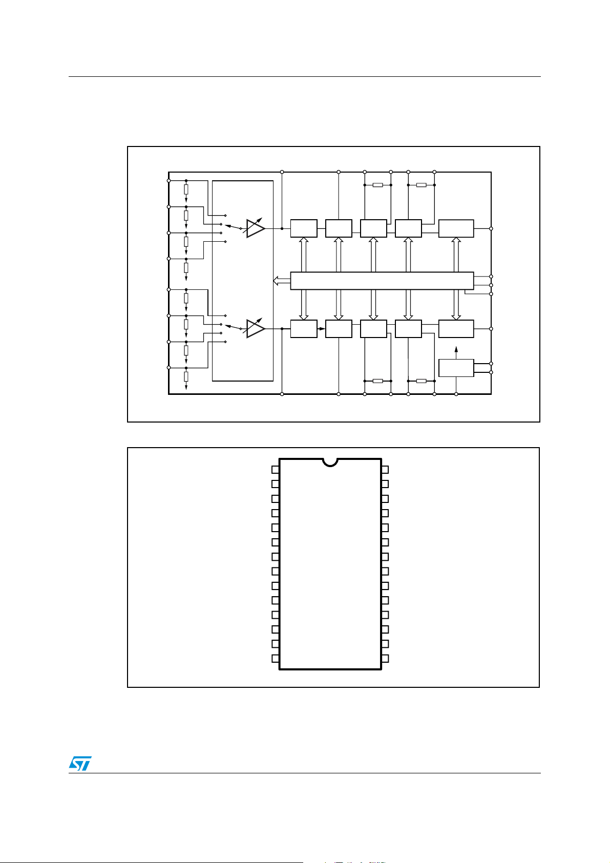
1 Block diagram and pin out
Figure 1. Block diagram
4
L-IN1
L-IN2
L-IN3
L-IN4
R-IN1
R-IN2
R-IN3
R-IN4
100K
5
100K
+ GAIN
G
0/30dB
2dB STEP
G
6
100K
7
100K
3
100K
2
100K
1
100K
28
100K
INPUT MULTIPLEXER
Figure 2. Pin connections
MUXOUTL
8 1817161415
VOLUME
VOLUME
9 191011121323
MUXOUTR
TREBLE(L)
TREBLE
TREBLE
TREBLE(R
MOUT(L)
MIN(L)
R
M
MIDDLE
I2CBUS DECODER + LATCHES
MIDDLE
R
M
MIN(R)MOUT(R
BIN(L)
BASS
BASS
BIN(R
R
B
R
B
BOUT(L)
SPKR ATT
SPKR ATT
BOUT(R
LEFT
RIGHT
V
REF
SUPPLY
CREF
27
21
22
20
26
24
25
LOUT
SCL
SDA
DIG_GND
ROUT
V
S
AGND
D97AU621
R_IN3
R_IN2
R_IN1
L_IN1
L_IN2 V
L_IN3
L_IN4
MUXOUTL
MUXOUTR
MIN(R)
MOUT(R)
BIN(R)
BOUT(R)
BIN(L)
1
2
3
4
5
6
7
8
9
10
11
12
13
14
D97AU622
28
27
26
25
24
22
21
20
19
18
17
16
15
R_IN4
LOUT
ROUT
AGND
S
CREF23
SDA
SCL
DIG-GND
TREBLE(R)
TREBLE(L)
MIN(L)
MOUT(L)
BOUT(L)
3/23
Electrical specifications TDA7439DS
2 Electrical specifications
Table 2. Absolute maximum ratings
Symbol Parameter Value Unit
Operating supply voltage 10.5 V
V
S
T
T
Table 3. Thermal data
Symbol Parameter Value Unit
Operating ambient temperature 0 to 70 °C
amb
Storage temperature range -55 to 150 °C
stg
R
th j-pin
Table 4. Quick reference data
Thermal resistance junction-pins 85 °C/W
Symbol Parameter Min. Typ Max Unit
V
Supply voltage 7 9 10.2 V
S
V
Max. input signal handling 2
CL
RMS
THD Total harmonic distortion V = 1 V RMS, f = 1 kHz 0.01 0.1 %
S/N Signal to noise ratio V
S
Channel separation f = 1 kHz 90 dB
C
= 1 V RMS (mode = OFF) 106 dB
out
Input gain (in 2 dB steps) 0 30 dB
Volume control (in 1 dB steps) -47 0 dB
Treble control (in 2 dB steps) -14 +14 dB
Middle control (in 2 dB steps) -14 +14 dB
Bass control (in 2 dB steps) -14 +14 dB
Balance control (in 1 dB steps) -79 0 dB
Mute attenuation 100 dB
Table 5. shows the electrical characteristics. Refer to the test circuit in Figure 3, T
25° C, V
= 9 V, RL= 10 kΩ, generator resistance Rg = 600 Ω, all controls flat (G = 0 dB),
S
amb
=
unless otherwise specified.
Table 5. Electrical characteristics
V
Symbol Parameter Test condition Min. Typ Max Unit
Supply
V
Supply voltage 7 9 10.2 V
S
I
Supply current 4 7 10 mA
S
SVR Ripple rejection 60 90 dB
4/23
TDA7439DS Electrical specifications
Table 5. Electrical characteristics (continued)
Symbol Parameter Test condition Min. Typ Max Unit
Input stage
V
G
in_min
G
in_max
G
R
S
Input resistance 70 100 130 kΩ
IN
Clipping level THD = 0.3% 2 2.5
CL
Input separation
IN
Minimum input gain -1 0 1 dB
Maximum input gain 29 30 31 dB
Step resolution 1.5 2 2.5 dB
step
Volu m e con t r o l
R
Volume control input resistance 20 33 50 kΩ
i
C
A
v_max
A
Volume control range 45 47 49 dB
range
Max. attenuation 45 47 49 dB
Step resolution 0.5 1 1.5 dB
step
E
Attenuation set error
A
EΤ Tracking error
V
A
Bass control
DC step
DC
Mute attenuation 80 100 dB
mute
(1)
V
RMS
The selected input is
grounded through a 2.2 µF
80 100 dB
capacitor
AV = 0 to -24 dB -1.0 0 1.0 dB
= -24 to -47 dB -1.5 0 1.5 dB
A
V
A
= 0 to -24 dB 0 1 dB
V
A
= -24 to -47 dB 0 2 dB
V
adjacent attenuation steps
from 0 dB to A
v_max
0
0.5
3mV
mV
Gb Control range Max. boost/cut ±12.0 ±14.0 ±16.0 dB
B
Treble control
Step resolution 1 2 3 dB
step
Internal feedback resistance 33 44 55 kΩ
R
B
(1)
Gt Control range Max. boost/cut ±13.0 ±14.0 ±15.0 dB
T
Mid-range control
Step resolution 1 2 3 dB
step
(1)
Gm Control range Max. boost/cut ±12.0 ±14.0 ±16.0 dB
M
R
Step resolution 1 2 3 dB
step
Internal feedback resistance 18.75 25 31.25 kΩ
M
5/23
Electrical specifications TDA7439DS
Table 5. Electrical characteristics (continued)
Symbol Parameter Test condition Min. Typ Max Unit
Speaker attenuators
C
S
V
A
Control range 70 76 82 dB
range
Step resolution 0.5 1 1.5 dB
step
E
A Attenuation set error
DC step Adjacent attenuation steps 0 3 mV
DC
Mute attenuation 80 100 dB
mute
Audio outputs
V
V
OUTDC
Clipping level d = 0.3% 2.1 2.6 Vrms
CLIP
Output load resistance 2 kΩ
R
L
R
Output impedance 10 40 70 Ω
O
DC voltage level 3.5 3.8 4.1 V
General
E
Output noise
NO
E
Total tracking error
t
S/N Signal to noise ratio
Channel separation, left/right 80 100 dB
S
C
dDistortion A
Bus input
V
Input low voltage 1 V
IL
V
Input high voltage 3 V
IH
I
Input current VIN = 0.4 V -5 0 5 µA
IN
Output voltage SDA
V
O
acknowledge
A
= 0 to -20 dB -1.5 0 1.5 dB
V
A
= -20 to -56 dB -2 0 2 dB
V
All gains = 0 dB;
BW = 20 Hz to 20 kHz flat
515µV
AV = 0 to -24 dB 0 1 dB
= -24 to -47 dB 0 2 dB
A
V
All gains 0 dB,
= 1 V RMS
V
O
= 0, VI = 1 V RMS 0.01 0.08 %
V
I
= 1.6 mA 0.4 0.8 V
O
95 106 dB
1. For bass, mid-range and treble response: the center frequency and the response quality can be set by the
external circuitry.
6/23
TDA7439DS Electrical specifications
Figure 3. Test circuit
2.7K 5.6K
5.6nF
18nF 22nF 100nF 100nF
0.47µF
0.47µF
0.47µF
0.47µF
0.47µF
0.47µF
0.47µF
0.47µF
L-IN1
L-IN2
L-IN3
L-IN4
R-IN1
R-IN2
R-IN3
R-IN4
4
100K
5
100K
6
100K
7
100K
3
100K
2
100K
1
100K
28
100K
MUXOUTL
G
0/30dB
2dB STEP
G
INPUT MULTIPLEXER
+ GAIN
MUXOUTR
TREBLE(L)
81817161415
VOLUME
VOLUME
9
TREBLE(R)
MIN(L)
MOUT(L)
BIN(L)
R
M
TREBLE
MIDDLE
BASS
I2CBUS DECODER + LATCHES
TREBLE
MIDDLE
BASS
R
M
19 10 11 12 13 23
MOUT(R) BOUT(R)BIN(R)
MIN(R)
18nF 22nF 100nF 100nF
5.6nF
2.7K 5.6K
BOUT(L)
R
B
SPKR ATT
LEFT
SPKR ATT
RIGHT
V
REF
SUPPLY
R
B
CREF
10µF
LOUT
27
21
SCL
22
SDA
20
DIGGND
26
ROUT
24
V
S
25
AGND
D98AU886
7/23

Application suggestions TDA7439DS
3 Application suggestions
The first and the last stages are volume control blocks. The control range is 0 to -47 dB and
mute for the first stage and 0 to -79 dB and mute for the last one. Both control blocks have a
step resolution of 1 dB.
This very high resolution allows the implementation of systems free from any noisy
acoustical effect.
The TDA7439DS audio processor provides 3 bands of tone control (bass, mid-range and
treble).
3.1 Tone control
3.1.1 Bass, mid-range stages
The bass and the mid-range cells have the same structure.
However, the bass cell has an internal resistor R
has an internal resistor R
of typically 25 kΩ.
M
of typically 44 kΩ whilst the mid-range cell
B
Several filter types can be implemented by connecting external components to the bass/mid
IN and OUT pins.
Typical responses are shown in Figure 8, Figure 9 and Figure 11.
Figure 4. Bass/mid-range filter implementation
Ri internal
OUTIN
R
2
D95AU313
C
2
C
1
Figure 4. refers to the basic T-type band-pass filter. Starting from the filter component values
(R1 (internal) and R2, C1, C2 (external)) then the centre frequency f
, the gain Av at
C
maximum boost and the filter Q factor are computed as follows:
f
---------------------------------------------------------------- -=
C
2 π R1 R2 C1 C2⋅⋅⋅⋅⋅
1
R2C2 R2C1 RiC1++
A
----------------------------------------------------------- -=
V
Q
8/23
R2C1 R2C2+
R1 R2 C1 C2⋅⋅⋅
-------------------------------------------------=
R2C1 R2C2+

TDA7439DS Application suggestions
Transposing and solving for the external components we get:
A
1–
C1
C2
R2
V
----------------------------------------- -=
2 π Fc Ri Q⋅⋅ ⋅ ⋅
2
C1⋅
Q
----------------------------- -=
1– Q2–
A
V
A
1– Q2–
--------------------------------------------------------------------- -=
2 π C1 Fc A
V
1–()Q⋅⋅⋅⋅ ⋅
V
3.1.2 Treble stage
The treble stage is a high-pass filter whose time constant is fixed by an internal resistor
(25 kΩ typically) and an external capacitor connected between treble pins and ground.
Typical responses are shown in Figure 10 and Figure 11.
3.2 Pin CREF
The suggested value of 10 µF for the reference capacitor (C
can be reduced to 4.7 µF if the application requires faster power-on.
3.3 Electrical characteristics
Figure 5. THD vs frequency Figure 6. THD vs R
), connected to pin CREF,
REF
LOAD
9/23

Application suggestions TDA7439DS
Figure 7. Channel separation vs
Figure 9. Mid-range filter response Figure 10. Treble filter response
frequency
Figure 8. Bass filter response
Figure 11. Typical tone response
10/23

TDA7439DS I2C bus interface
4 I2C bus interface
Data transmission from the microprocessor to the TDA7439DS and vice versa takes place
through the 2-wire I
Pull-up resistors to the positive supply voltage must be used (there are no internal pull-ups).
2
C bus interface. This consists of the data and clock lines, SDA and SCL.
4.1 Data validity
The data on the SDA line must be stable during the high period of the clock as shown in
Figure 12. SDA is allowed to change only when SCL is low.
4.2 Start and stop conditions
As shown in Figure 13 a start condition is a high to low transition of SDA while SCL is high.
The stop condition is a low to high transition of SDA while SCL is high.
4.3 Byte format
Every byte transferred on the SDA line must contain 8 bits. The MSB is transferred first.
There is also provision for an acknowledge bit to follow each byte to indicate that the data
has been received.
4.4 Acknowledge
The master (µP) puts a resistive high level on SDA during the acknowledge clock pulse (see
Figure 14). The peripheral (audio processor) that acknowledges has to pull down (low) the
SDA line during this clock pulse.
The audio processor which has been addressed has to generate an acknowledge after the
reception of each byte, otherwise the SDA line remains at the HIGH level during the ninth
clock pulse time. In this case the master transmitter can generate the STOP information in
order to abort the transfer.
4.5 Transmission without acknowledge
Suppressing the audio processor acknowledge detection enables the µP to use a simpler
transmission: it simply waits for one clock, without checking the slave acknowledging, and
then sends the new data.
This approach has, of course, less protection from transmission errors.
11/23

I2C bus interface TDA7439DS
Figure 12. Timing diagram of the data on the I2C bus
SCL
SDA
Data can changeData stable
when clock high when clock low
Figure 13. Timing diagram of the start/stop
SCL
SDA
Start
Figure 14. Timing diagram of the acknowledge
SCL
SDA
MSB
Start
4.6 Interface protocol
The interface protocol comprises:
" a start condition (S)
" a chip-address byte, containing the TDA7439DS address
" a sub-address byte including an auto address-increment bit
" a sequence of data bytes (N bytes + acknowledge)
" a stop condition (P).
Stop
1
2
6
7
8
9
Acknowledge
from receiver
Figure 15. SDA addressing and data
CHIP ADDRESS
MSB
S 1 0 0 0 1 0 0 0 ACK ACK DATA ACK P
D96AU420
S = Start, ACK = Acknowledge, B = Auto increment, P = Stop
LSB MSB LSB MSB LSB
12/23
SUBADDRESS DATA 1 to DATA n
XXB
X
DATA

TDA7439DS I2C bus transmission examples
5 I2C bus transmission examples
5.1 No address incrementing
The TDA7439DS receives a start condition followed by the correct chip address, then a sub
address with the bit B = 0 (for no address increment), then the data bytes to be sent to the
sub address and finally a stop condition.
Figure 16. SDA addressing and data for B = 0
CHIP ADDRESS
MSB
S 1 0 0 0 1 0 0 0 ACK ACK DATA ACK P
D96AU421
LSB MSB LSB MSB LSB
5.2 Address incrementing
The TDA7439DS receives a start condition followed by the correct chip address, then a sub
address with the B = 1 for address incrementing; now it is in a loop condition with an
automatic increase of the sub address up to D[3:0] = 0x7. That is, the data for sub
addresses from D[3:0] = 1000 (binary) to 1111 are ignored.
In Figure 17 below, DATA1 is directed to the sub address sent (that is, D[3:0]), DATA2 is
directed to the sub address incremented by 1 (that is, 1 + D[3:0]) and so forth until a stop
condition is received to terminate the transmission.
Figure 17. SDA addressing and data for B = 1
CHIP ADDRESS
MSB
S 1 0 0 0 1 0 0 0 ACK ACK DATA ACK P
D96AU422
LSB MSB LSB MSB LSB
SUBADDRESS DATA
0
X
D3
1
D3
D2 D1 D0
D2 D1 D0
X
X
SUBADDRESS DATA 1 to DATA n
X
X
X
Table 6. Power-on-reset conditions
Parameter POR value
Input selection IN2
Input gain 28 dB
Volume MUTE
Bass 0 dB
Mid-range 2 dB
Tr e bl e 2 d B
Speaker MUTE
13/23

I2C bus addresses and data TDA7439DS
6 I2C bus addresses and data
6.1 Chip address byte
The TDA7439DS chip address is 0x88.
6.2 Sub-address byte
The function is selected by the 4-bit sub address as given in Ta bl e 7 . The three MSBs are
not used and bit D4 selects address incrementing (B = 1) or single data byte (B = 0).
Table 7. Function selection: sub-address byte
MSB LSB
Function
D7 D6 D5 D4 D3 D2 D1 D0
X X X B 0 0 0 0 Input selector
X X X B 0 0 0 1 Input gain
XXXB0 0 1 0Volume
XXXB0 0 1 1Bass gain
X X X B 0 1 0 0 Mid-range gain
XXXB0 1 0 1Treble gain
X X X B 0 1 1 0 Speaker attenuation, R
X X X B 0 1 1 1 Speaker attenuation, L
6.3 Data bytes
The function value is changed by the data byte as given in the following tables, Ta bl e 8 to
Ta bl e 1 4.
In the tables of input gain, volume and attenuation, not all values are shown. A desired
intermediate value is obtained by setting the three LSBs to the appropriate value.
Table 8. Input selector value (sub address 0x0)
MSB LSB
D7 D6 D5 D4 D3 D2 D1 D0
XXXXXX0 0 IN4
XXXXXX0 1 IN3
XXXXXX1 0 IN2
XXXXXX1 1 IN1
Input multiplexer
14/23

TDA7439DS I2C bus addresses and data
Table 9. Input gain value (sub address 0x1)
MSB LSB
D7 D6 D5 D4 D3 D2 D1 D0
Input gain
2-dB steps
XXXX0 0 0 0 0dB
XXXX0 0 0 1 2dB
XXXX0 0 1 0 4dB
XXXX0 0 1 1 6 dB
XXXX0 1 0 0 8dB
XXXX0 1 0 1 10dB
XXXX0 1 1 0 12dB
XXXX0 1 1 1 14dB
XXXX1 0 0 0 16dB
XXXX1 0 0 1 18dB
XXXX1 0 1 0 20dB
XXXX1 0 1 1 22dB
XXXX1 1 0 0 24dB
XXXX1 1 0 1 26dB
XXXX1 1 1 0 28dB
XXXX1 1 1 1 30dB
Table 10. Volume value (sub address 0x2)
MSB LSB
D7 D6 D5 D4 D3 D2 D1 D0
Volume
1-dB steps
X0000000 0dB
X0000001 -1dB
X0000010 -2dB
X0000011 -3dB
X0000100 -4dB
X0000101 -5dB
X0000110 -6dB
X0000111 -7dB
X0001000 -8dB
X0010000 -16dB
X0011000 -24dB
X0100000 -32dB
X0101000 -40dB
XX1 1 1XXX MUTE
15/23
I2C bus addresses and data TDA7439DS
Table 11. Bass gain value (sub address 0x3)
MSB LSB
D7 D6 D5 D4 D3 D2 D1 D0
Bass gain
2-dB steps
XXXX0 0 0 0 -14dB
XXXX0 0 0 1 -12dB
XXXX0 0 1 0 -10dB
XXXX0 0 1 1 -8dB
XXXX0 1 0 0 -6dB
XXXX0 1 0 1 -4dB
XXXX0 1 1 0 -2dB
XXXXX1 1 1 0dB
XXXX1 1 1 0 2dB
XXXX1 1 0 1 4dB
XXXX1 1 0 0 6dB
XXXX1 0 1 1 8dB
XXXX1 0 1 0 10dB
XXXX1 0 0 1 12dB
XXXX1 0 0 0 14dB
Table 12. Mid-range gain value (sub address 0x4)
MSB LSB
D7 D6 D5 D4 D3 D2 D1 D0
Mid-range gain
2-dB steps
XXXX0 0 0 0 -14dB
XXXX0 0 0 1 -12dB
XXXX0 0 1 0 -10dB
XXXX0 0 1 1 -8dB
XXXX0 1 0 0 -6dB
XXXX0 1 0 1 -4dB
XXXX0 1 1 0 -2dB
XXXXX1 1 1 0dB
XXXX1 1 1 0 2dB
XXXX1 1 0 1 4dB
XXXX1 1 0 0 6dB
XXXX1 0 1 1 8dB
XXXX1 0 1 0 10dB
XXXX1 0 0 1 12dB
XXXX1 0 0 0 14dB
16/23

TDA7439DS I2C bus addresses and data
Table 13. Treble gain value (sub address 0x5)
MSB LSB
D7 D6 D5 D4 D3 D2 D1 D0
Treble gain
2-dB steps
XXXX0 0 0 0 -14dB
XXXX0 0 0 1 -12dB
XXXX0 0 1 0 -10dB
XXXX0 0 1 1 -8dB
XXXX0 1 0 0 -6dB
XXXX0 1 0 1 -4dB
XXXX0 1 1 0 -2dB
XXXXX1 1 1 0dB
XXXX1 1 1 0 2dB
XXXX1 1 0 1 4dB
XXXX1 1 0 0 6dB
XXXX1 0 1 1 8dB
XXXX1 0 1 0 10dB
XXXX1 0 0 1 12dB
XXXX1 0 0 0 14dB
Table 14. Speaker attenuation value (sub address 0x6, 0x7)
MSB LSB
D7 D6 D5 D4 D3 D2 D1 D0
Speaker attenuation
1-dB steps
X0000000 0dB
X0000001 1dB
X0000010 2dB
X0000011 3dB
X0000100 4dB
X0000101 5dB
X0000110 6dB
X0000111 7dB
X0001000 8dB
X0010000 16dB
X0011000 24dB
X0100000 32dB
X0101000 40dB
X0110000 48dB
X0111000 56dB
17/23
I2C bus addresses and data TDA7439DS
Table 14. Speaker attenuation value (sub address 0x6, 0x7) (continued)
MSB LSB
D7 D6 D5 D4 D3 D2 D1 D0
X1000000 64dB
X1001000 72dB
X1111XXX MUTE
Speaker attenuation
1-dB steps
18/23

TDA7439DS Chip input/output circuits
)
)
7 Chip input/output circuits
Figure 18. Pin 23 Figure 19. Pins 26, 27
V
S
V
V
S
S
24
CREF
20K
ROUT
LOUT
D96AU434
V
S
20µA
V
20K
D96AU430
Figure 20. Pins 1, 2, 3, 4, 5, 6, 7, 28 Figure 21. Pins 8, 9
V
S
20µA
IN
MIXOUT
100K
V
REF
Figure 22. Pins 11, 16 Figure 23. Pins 10, 17
V
S
D96AU425
V
S
S
20µA
GND
D96AU426
MOUT(L)
MOUT(R
25K
20µA
D96AU431
20µA
25K
MIN(L)
MIN(R
D96AU431
19/23

Chip input/output circuits TDA7439DS
)
Figure 24. Pins 12, 14 Figure 25. Pins 13, 15
V
S
20µA
V
S
20µA
44K
BIN(L)
BIN(R) D96AU428
Figure 26. Pins 18, 19 Figure 27. Pin 21
V
S
BOUT(L)
BOUT(R
20µA
TREBLE(L)
SCL
TREBLE(R)
50K
D96AU433
Figure 28. Pin 22
20µA
44K
D96AU429
20µA
D96AU424
SDA
D96AU423
20/23

TDA7439DS Package information
8 Package information
DIM.
A 2.65 0.104
a1 0.1 0.3 0.004 0.012
b 0.35 0.49 0.014 0.019
b1 0.23 0.32 0.009 0.013
C 0.5 0.020
c1 45° (typ.)
D 17.7 18.1 0.697 0.713
E 10 10.65 0.394 0.419
e 1.27 0.050
e3 16.51 0.65
F 7.4 7.6 0.291 0.299
L 0.4 1.27 0.016 0.050
S8
mm inch
MIN. TYP. MAX. MIN. TYP. MAX.
(max.)
°
OUTLINE AND
Outline and mechanical data
MECHANICAL DATA
SO28
SO-28
21/23

Revision history TDA7439DS
9 Revision history
Table 15. Document revision history
Date Revision Changes
Jan-2004 1 Initial release
Jun-2004 2 Modified presentation
14-Nov-2007 3
20-Nov-2007 4 Updated Figure 23 and Figure 27
Updated titles to Figure 9 and Figure 10
Minor updates to presentation
22/23

TDA7439DS
Please Read Carefully:
Information in this document is provided solely in connection with ST products. STMicroelectronics NV and its subsidiaries (“ST”) reserve the
right to make changes, corrections, modifications or improvements, to this document, and the products and services described herein at any
time, without notice.
All ST products are sold pursuant to ST’s terms and conditions of sale.
Purchasers are solely responsible for the choice, selection and use of the ST products and services described herein, and ST assumes no
liability whatsoever relating to the choice, selection or use of the ST products and services described herein.
No license, express or implied, by estoppel or otherwise, to any intellectual property rights is granted under this document. If any part of this
document refers to any third party products or services it shall not be deemed a license grant by ST for the use of such third party products
or services, or any intellectual property contained therein or considered as a warranty covering the use in any manner whatsoever of such
third party products or services or any intellectual property contained therein.
UNLESS OTHERWISE SET FORTH IN ST’S TERMS AND CONDITIONS OF SALE ST DISCLAIMS ANY EXPRESS OR IMPLIED
WARRANTY WITH RESPECT TO THE USE AND/OR SALE OF ST PRODUCTS INCLUDING WITHOUT LIMITATION IMPLIED
WARRANTIES OF MERCHANTABILITY, FITNESS FOR A PARTICULAR PURPOSE (AND THEIR EQUIVALENTS UNDER THE LAWS
OF ANY JURISDICTION), OR INFRINGEMENT OF ANY PATENT, COPYRIGHT OR OTHER INTELLECTUAL PROPERTY RIGHT.
UNLESS EXPRESSLY APPROVED IN WRITING BY AN AUTHORIZED ST REPRESENTATIVE, ST PRODUCTS ARE NOT
RECOMMENDED, AUTHORIZED OR WARRANTED FOR USE IN MILITARY, AIR CRAFT, SPACE, LIFE SAVING, OR LIFE SUSTAINING
APPLICATIONS, NOR IN PRODUCTS OR SYSTEMS WHERE FAILURE OR MALFUNCTION MAY RESULT IN PERSONAL INJURY,
DEATH, OR SEVERE PROPERTY OR ENVIRONMENTAL DAMAGE. ST PRODUCTS WHICH ARE NOT SPECIFIED AS "AUTOMOTIVE
GRADE" MAY ONLY BE USED IN AUTOMOTIVE APPLICATIONS AT USER’S OWN RISK.
Resale of ST products with provisions different from the statements and/or technical features set forth in this document shall immediately void
any warranty granted by ST for the ST product or service described herein and shall not create or extend in any manner whatsoever, any
liability of ST.
ST and the ST logo are trademarks or registered trademarks of ST in various countries.
Information in this document supersedes and replaces all information previously supplied.
The ST logo is a registered trademark of STMicroelectronics. All other names are the property of their respective owners.
© 2007 STMicroelectronics - All rights reserved
STMicroelectronics group of companies
Australia - Belgium - Brazil - Canada - China - Czech Republic - Finland - France - Germany - Hong Kong - India - Israel - Italy - Japan -
Malaysia - Malta - Morocco - Singapore - Spain - Sweden - Switzerland - United Kingdom - United States of America
www.st.com
23/23
 Loading...