


DUALLOW-VOLTAGE POWER AMPLIFIER
.
SUPPLYVOLTAGE DOWN TO 1.8V
.
LOW CROSSOVERDISTORSION
.
LOW QUIESCENTCURRENT
.
BRIDGE ORSTEREOCONFIGURATION
DESCRIPTION
TheTDA2822Mis amonolithicintegratedcircuit in
8 lead Minidip package. It is intended for use as
dual audio power amplifier in portable cassette
playersand radios.
TDA2822M
MINIDIP
ORDERING NUMBER : TDA2822M
PIN CONNECTION (Top view)
March 1995
1/11

TDA2822M
SCHEMATIC DIAGRAM
ABSOLUTE MAXIMUM RATINGS
Symbol Parameter Value Unit
Supply Voltage 15 V
Peak Output Current 1 A
Total Power Dissipation at T
at T
amb
case
=50°C
=50°C
1
1.4
Storage and Junction Temperature – 40, + 150 °C
P
T
stg,Tj
V
s
I
o
tot
THERMALDATA
Symbol Parameter Value Unit
R
th j-amb
R
th j-case
Thermal Resistance Junction-ambient Max. 100 °C/W
Thermal Resistance Junction-pin (4) Max. 70 °C/W
W
W
2/11

TDA2822M
ELECTRICALCHARACTERISTICS (VS=6V,T
=25oC, unlessotherwisespecified)
amb
Symbol Parameter Test Conditions Min. Typ. Max. Unit
STEREO (test circuit of Figure 1)
V
V
P
G
∆G
e
Supply Voltage 1.8 15 V
s
Quiescent Output Voltage
o
I
Quiescent Drain Current 6 9 mA
d
I
Input Bias Current 100 nA
b
Output Power (each channel)
o
(f = 1kHz, d = 10%) R
d Distortion (f = 1kHz) R
Closed Loop Voltage Gain f = 1kHz 36 39 41 dB
v
Channel Balance ± 1dB
v
R
Input Resistance f = 1kHz 100 kΩ
i
Total Input Noise Rs= 10kΩ B = Curve A
N
=3V
V
s
=32Ω VS=9V
L
=16Ω VS=6V
R
L
=8Ω VS=9V
R
L
=4Ω VS=6V
R
L
=32Ω Po= 40mW
L
=16Ω Po= 75mW
R
L
=8Ω Po= 150mW
R
L
V
V
V
V
V
V
V
=6V
S
= 4.5V
S
=3V
S
=2V
S
=6V
S
= 4.5V
S
=3V
S
B = 22Hz to 22kHz
90
15
170
300
450
2.7
1.2
300
120
60
20
5
220
1000
380
650
320
110
0.2
0.2
0.2
2
2.5
V
V
mW
%
%
%
µV
µV
SVR Supply Voltage Rejection f = 100Hz, C1 = C2 = 100µF2430 dB
C
Channel Separation f = 1kHz 50 dB
s
BRIDGE (test circuit of Figure 2)
V
V
P
G
e
Supply Voltage 1.8 15 V
s
I
Quiescent Drain Current RL= ∞ 69mA
d
Output Offset Voltage
os
(between the outputs)
Input Bias Current 100 nA
I
b
Output Power (f = 1kHz, d = 10%)
o
d Distortion P
Closed Loop Voltage Gain f = 1kHz 39 dB
v
R
Input Resistance f = 1kHz 100 kΩ
i
Total Input Noise Rs= 10kΩ B = Curve A
N
RL=8Ω ±50 mV
=32Ω VS=9V
R
L
=16Ω VS=9V
R
L
=8Ω VS=6V
R
L
=4Ω VS= 4.5V
R
L
= 0.5W, RL=8Ω, f = 1kHz 0.2 %
o
V
V
V
V
V
V
V
V
V
V
=6V
S
= 4.5V
S
=3V
S
=2V
S
=6V
S
=3V
S
= 4.5V
S
=3V
S
=3V
S
=2V
S
320
50
900
200
1000
400
200
65
8
2000
800
120
1350
700
220
1000
350
80
2.5
B = 22Hz to 22kHz
3
mW
µV
µV
SVR Supply Voltage Rejection f = 100Hz 40 dB
B Power Bandwidth (–3dB) R
=8Ω,Po= 1W 120 kHz
L
3/11

TDA2822M
Figure1 : TestCircuit (Stereo)
Figure2 : TestCircuit (Bridge)
Figure3 : P.C.Board and Components Layout
of the Circuitof Figure1
4/11
Figure 4 : P.C. Boardand ComponentsLayout
of theCircuit of Figure 2

TDA2822M
Figure5 : QuiescentCurrentversus
SupplyVoltage
Figure7 : OutputPower versus SupplyVoltage
(THD = 10%, f = 1kHz Stereo)
Figure 6 : SupplyVoltage Rejectionversus
Frequency
Figure 8 : Distorsion versus OutputPower
(Stereo)
Figure9 : Distorsion versusOutput Power
(Stereo)
Figure 10 : Output Power versusSupplyVoltage
(Bridge)
5/11
TDA2822M
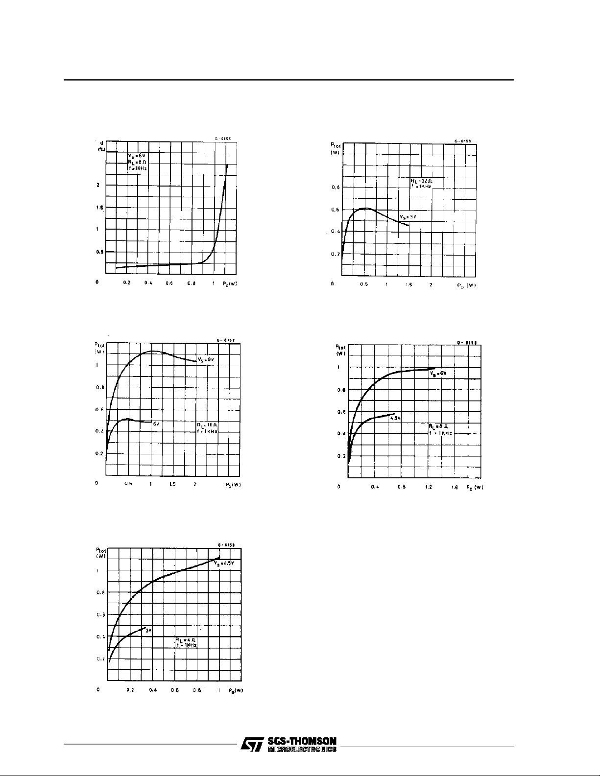
Figure11 : Distorsion versusOutputPower
(Bridge)
Figure13 : TotalPowerDissipation versus
OutputPower(Bridge)
Figure 12 : Total PowerDissipation versus
Output Power(Bridge)
Figure 14 : Total PowerDissipation versus
Output Power(Bridge)
Figure15 : TotalPowerDissipation versus
OutputPower(Bridge)
6/11

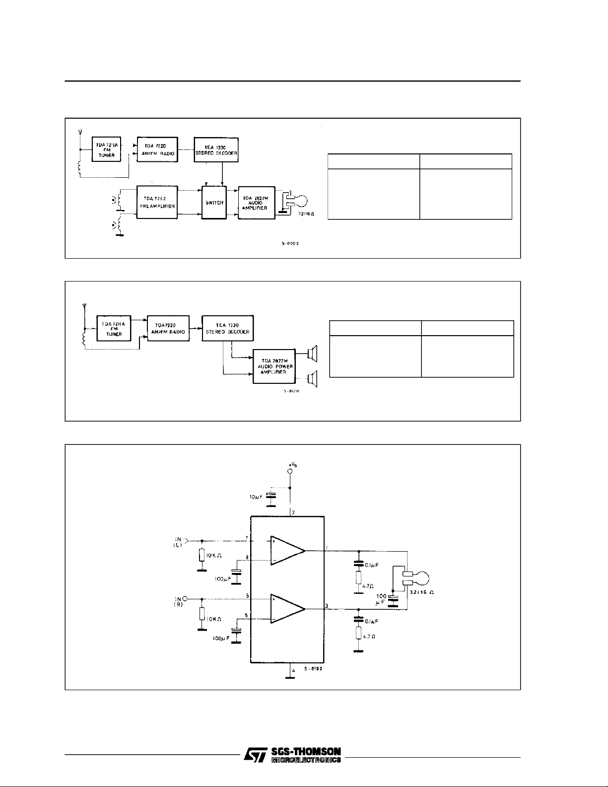
Figure16 : TypicalApplicationin PortablePlayers
TDA2822M
Figure17 : ApplicationinPortable Radio Receivers
7/11
TDA2822M
Figure18 : PortableRadio CassettePlayers
Figure19 : Portable StereoRadios
Type Supply Voltage
TDA 7220
TDA 7211A
TEA 1330
TDA 7282
TDA 2822M
Type Supply Voltage
TDA 7220
TDA 7211A
TEA 1330
TDA 2822M
1.5 V to 6 V
1.2 V to 6 V
3 V to 15 V
1.5 V to 6 V
1.8 V to 15 V
1.5Vto6V
1.2Vto6V
3 V to 15 V
1.8 V to 15 V
Figure20 : Low Cost Applicationin Portable Players (usingonly one 100µF outputcapacitor)
8/11

Figure21 : 3V Stereo Cassette PlayerwithMotot Speed Control
TDA2822M
9/11
TDA2822M
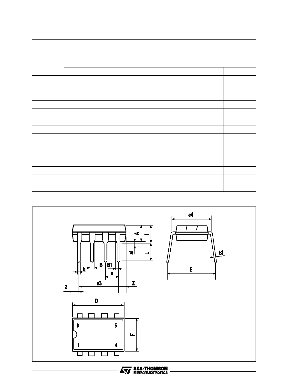
MINIDIPPACKAGE MECHANICAL DATA
DIM.
MIN. TYP. MAX. MIN. TYP. MAX.
A 3.32 0.131
a1 0.51 0.020
B 1.15 1.65 0.045 0.065
b 0.356 0.55 0.014 0.022
b1 0.204 0.304 0.008 0.012
D 10.92 0.430
E 7.95 9.75 0.313 0.384
e 2.54 0.100
e3 7.62 0.300
e4 7.62 0.300
F 6.6 0.260
I 5.08 0.200
L 3.18 3.81 0.125 0.150
Z 1.52 0.060
mm inch
10/11

TDA2822M
Information furnished is believed to be accurate and reliable. However,SGS-THOMSON Microelectronicsassumes no responsibility
for the consequences of use of such information norfor anyinfringement ofpatents or other rights of third parties which may result
from its use. No license isgrantedbyimplication or otherwise under any patent or patent rights ofSGS-THOMSON Microelectronics.
Specifications mentioned in this publication are subject to change without notice. This publication supersedes and replaces all
information previously supplied.SGS-THOMSON Microelectronics products arenot authorized for useas critical components in life
support devices or systems without express written approval of SGS-THOMSON Microelectronics.
1994 SGS-THOMSON Microelectronics - All Rights Reserved
Australia- Brazil - France - Germany- Hong Kong - Italy - Japan - Korea- Malaysia - Malta- Morocco - The Netherlands- Singa-
pore - Spain- Sweden - Switzerland - Taiwan - Thaliand - United Kingdom -U.S.A.
SGS-THOMSON Microelectronics GROUP OF COMPANIES
11/11
 Loading...