

TDA2822D
DUAL LOW-VOLTAGE POWER AMPLIFIER
SUPPLYVOLTAGEDOWN TO 1.8V
LOWCROSSOVERDISTORTION
LOW QUIESCENT CURRENT
BRIDGEOR STEREOCONFIGURATION
DESCRIPTION
The TDA2822D is a monolithic integrated circuit
in 8 lead (SO-8)package. It is intendedfor use as
dual audio power amplifier in portable cassette
ORDERING NUMBER: TDA2822D
players,radios and CD players
ABSOLUTE MAXIMUM RATINGS
Symbol Parameter Value Unit
Supply Voltage 15 V
S
Peak Output 1 A
Total Power Dissipation T
Storage and JunctionTemperature -40 to 150 °C
=50°C 0.5 W
amb
P
T
stg,Tj
V
I
O
tot
SO8
APPLICATIONCIRCUIT
May 1991
1/6

TDA2822D
PIN CONNECTION (Topview)
THERMAL DATA
Symbol Description Value Unit
R
th j-amb
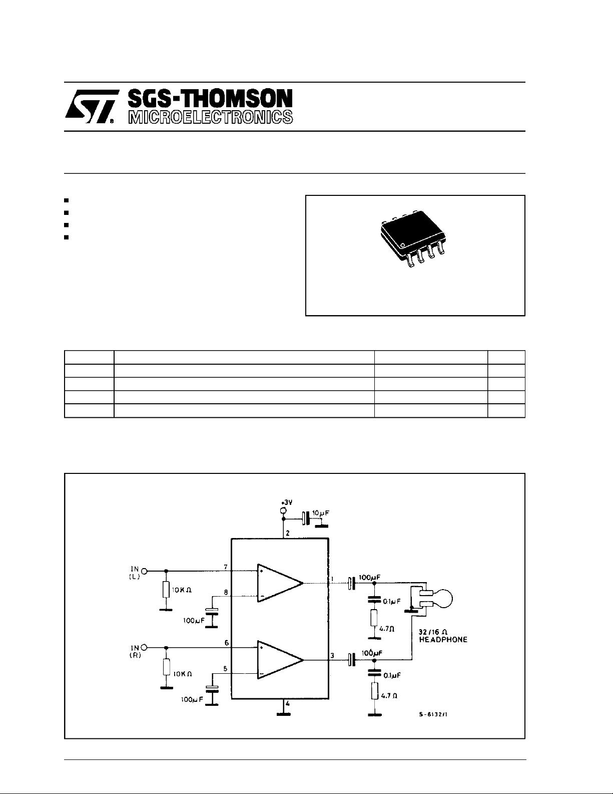
Figure1: Stereo Applicationand Test Circuit
Thermal Resistance Junction-ambient Max 200 °C/W
Figure2: Bridge Applicationand Test Circuit
2/6

TDA2822D
ELECTRICAL CHARACTERISTICS (VS= 6V; T
=25°C,unless otherwisespecified.
amb
STEREO(Test circuitof fig. 1).
Symbol Parameter Test Condition Min. Typ. Max. Unit
V
S
I
d
V
O
I
b
P
O
d Distortion R
G
V
∆G
R
e
N
Supply Voltage 1.8 15 V
Total QuiescentDrain Current 15 mA
Quiescent Output Voltage 2.7 V
= 3V 1.2 V
V
S
Input Bias Current 100 nA
Output Power (eachchannel)
(f = 1KHz, d = 10%)
R
=32Ω VS= 4.5V
L
R
=16Ω VS= 6V 170 220 mW
L
R
=8Ω VS= 6V 300 380 mW
L
R
=4Ω VS= 4.5V
L
=32Ω PO= 40mW 0.2 %
L
=16Ω PO= 75mW 0.2 %
R
L
R
=8Ω PO= 150mW 0.2 %
L
VS=9V
V
=6V
S
V
=3V
S
V
=2V
S
V
=3V
S
300
120
60
20
5
320
110
Closed Loop VoltageGain f = 1KHz 36 39 41 dB
Channel Balance ±1dB
V
Input Resistance f = 1KHz 100 KΩ
i
Total Input Noise Rs= 10kΩ B = Curve A 2 µV
= 10kΩ B = 22Hz to 22KHz 2.5 µV
R
s
SVR Supply Voltage Rejection f = 100Hz C1 = C2 = 100µF24 30 dB
C
s
Channel Separation f = 1KHz 50 dB
BRIDGE(Test circuitof fig.2)
mW
mW
mW
V
S
I
d
V
os
Supply Voltage 1.8 15 V
Total QuiescentDrain Current RL= ∞ 15 mA
Output Offset Voltage(between
RL=8Ω ±80 mV
the outputs)
I
b
P
O
d Distortion R
G
V
R
e
N
Input Bias Current 100 nA
Output Power
(f = 1KHz, d = 10%)
R
=32Ω VS= 4.5V
L
R
=16Ω VS=6V
L
RL = 16W V
R
=8Ω VS= 4.5V
L
RL = 8W V
R
=4Ω VS=3V
L
RL = 4W V
=8Ω PO= 0.5W f = 1KHz 0.2 %
L
VS=9V
V
=6V
S
V
=3V
S
V
=2V
S
=3V
S
=3V
S
=2V
S
320
50
1000
400
200
65
8
800
120
700
220
350
80
Closed Loop VoltageGain f = 1KHz 39 dB
Input Resistance f = 1KHz 100 KΩ
i
Total Input Noise Rs= 10kΩ B = Curve A 2.5 µV
R
= 10kΩ B = 22Hz to 22KHz 3 µV
s
mW
mW
mW
mW
mW
mW
mW
SVR Supply Voltage Rejection f = 100Hz 40 dB
B Power Bandwidth (-3dB) R
=8Ω PO= 1W 120 KHz
L
3/6

TDA2822D
Figure3: Supply VoltageRejection vs. Fre-
quency
Figure5: Total Power Dissipation vs. Output
Power (Bridge)
Figure4: Output Power vs.Supply Voltage(THD
= 10%, f =1KHz Stereo)
Figure6: TotalPower Dissipationvs. Output
Power(Bridge)
4/6

SO8 PACKAGE MECHANICAL DATA
TDA2822D
DIM.
MIN. TYP. MAX. MIN. TYP. MAX.
A 1.75 0.069
a1 0.1 0.25 0.004 0.010
a2 1.65 0.065
a3 0.65 0.85 0.026 0.033
b 0.35 0.48 0.014 0.019
b1 0.19 0.25 0.007 0.010
C 0.25 0.5 0.010 0.020
c1 45° (typ.)
D 4.8 5.0 0.189 0.197
E 5.8 6.2 0.228 0.244
e 1.27 0.050
e3 3.81 0.150
F 3.8 4.0 0.15 0.157
L 0.4 1.27 0.016 0.050
M 0.6 0.024
S8°(max.)
mm inch
5/6

TDA2822D
Information furnished is believed to be accurate and reliable. However, SGS-THOMSON Microelectronics assumes no responsibility for the
consequences of use of such information nor for any infringement ofpatents or otherrights ofthird parties which may resultfrom its use. No
license is granted by implication or otherwise under any patent or patent rights of SGS-THOMSON Microelectronics. Specifications mentioned in this publication are subject to change without notice. This publication supersedes and replaces all information previously supplied.
SGS-THOMSON Microelectronics products are not authorized for use as critical components in life support devices or systems without express written approval of SGS-THOMSON Microelectronics.
1994 SGS-THOMSON Microelectronics - All RightsReserved
SGS-THOMSON Microelectronics GROUP OF COMPANIES
Australia - Brazil- France - Germany - Hong Kong - Italy - Japan- Korea - Malaysia - Malta - Morocco - The Netherlands- Singapore -
Spain -Sweden - Switzerland - Taiwan- Thaliand- United Kingdom - U.S.A.
6/6
 Loading...