

现货库存、技术资料、百科信息、热点资讯,精彩尽在鼎好!
60W Hi-Fi AUDIO POWER AMPLIFIER
SUPPLYVOLTAGERANGEUP TO±25V
SPLIT SUPPLY OPERATION
HIGHOUTPUT POWER
(UP TO 60W MUSICPOWER)
LOW DISTORTION
MUTE/STAND-BY FUNCTION
NO SWITCH ON/OFF NOISE
AC SHORT CIRCUIT PROTECTION
THERMALSHUTDOWN
ESDPROTECTION
TDA2052
WITH MUTE / STAND-BY
Heptawatt
ORDERING NUMBER: TDA2052
DESCRIPTION
The TDA2052 is a monolithic integrated circuit in
Heptawatt package, intended for use as audio
class AB amplifier in TV or Hi-Fi field application.
Thanks to the wide voltage range and to the high
out current capability it’s able to supply the high-
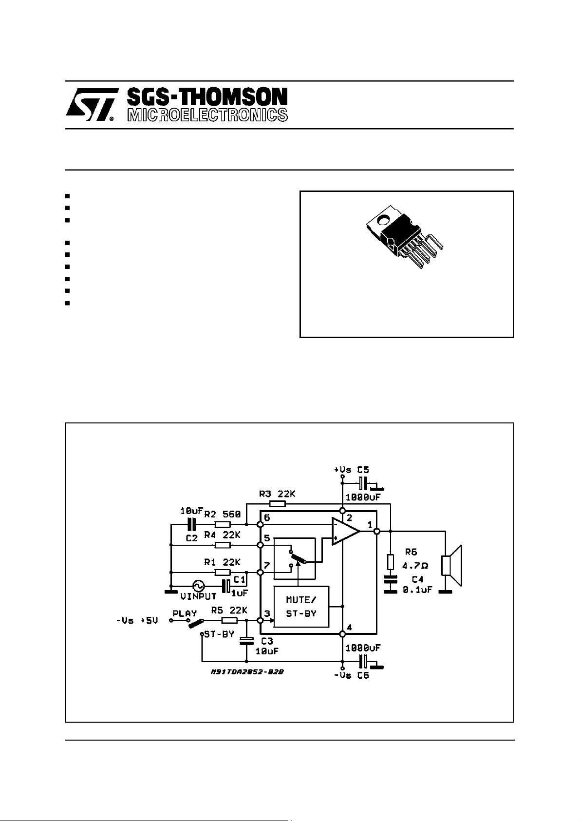
TEST ANDAPPLICATION CIRCUIT
est power into both 4Ωand 8Ωloads even in
presenceof poorsupply regulation.
The built in Muting/Stand-by function simplifies
the remote operations avoiding also switchingonoff noises.
February 1997
This is advanced information on a new product now in developmentor undergoing evaluation. Detailsare subject to changewithoutnotice.
1/13
TDA2052
ABSOLUTE MAXIMUM RATINGS
Symbol Parameter Value Unit
V
I
O
P
tot
T
op
T
stg,Tj
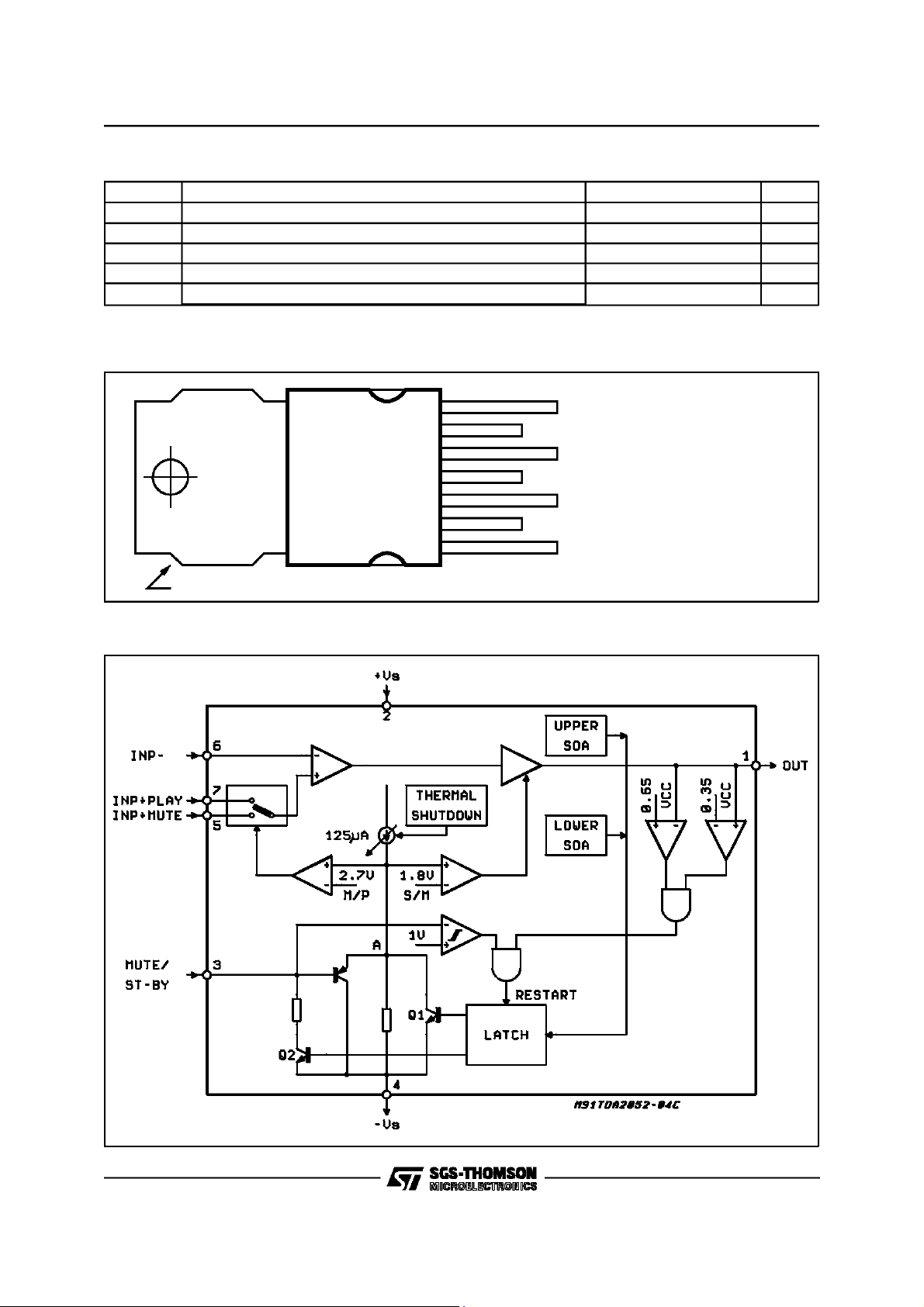
PIN CONNECTION (Topview)
DC Supply Voltage ±25 V
S
Output PeakCurrent (internally limited) 6 A
Power DissipationT
=70°C30W
case
Operating Temperature Range 0 to +70 °C
Storage and Junction Temperature -40 to +150
7 NON INVERTING INPUT(PLAY)
6
5
4
3
2
1
INVERTING INPUT
NON INVERTING INPUT(MUTE)
-V
S
STAND-BY/MUTE
+V
S
OUTPUT
C
°
tab connected to pin 4
BLOCK DIAGRAM
D95AU326
2/13
TDA2052
THERMAL DATA
Symbol Description Value Unit
R
th j-case
Thermal ResistanceJunction-case Max 2.5
C/W
°
ELECTRICAL CHARACTERISTICS (Refer to the test circuit, GV= 32dB; VS+ 18V; f = 1KHz; T
25°C, unlessotherwise specified.)
Symbol Parameter Test Condition Min. Typ. Max. Unit
V
S
I
q
I
b
V
OS
I
OS
P
O
P
O
Supply Range +6 +25 V
Total Quiescent Current VS= +22V 20 40 70 mA
Input Bias Current +0.5 µA
Input Offset Voltage +15 mV
Input Offset Current +200 nA
Music Output Power
IEC268-3 Rules (*)
VS= + 22.5, RL=4Ω,
d = 10%, t = 1s 50 60 W
Output Power(continuous RMS) d = 10%
RL = 4Ω
R
=8
Ω
L
V
= +22V, RL=8Ω
S
35
30
40
22
33
d=1%
d Total Harmonic Distortion R
R
=4Ω
L
R
=8
Ω
L
V
= +22V, RL=8Ω
S
=4Ω
L
P
= 0.1 to 20W;
O
f = 100Hz to 15KHz
+ 22V, RL=8Ω
V
S
P
= 0.1 to 20W;
O
f = 100Hz to 15KHz
32
17
28
0.1
0.1
0.7
0.5
SR Slew Rate 3 5 V/µs
G
V
e
N
R
SVR Supply Voltage Rejection f = 100Hz, V
T
S
Open Loop Voltage Gain 80 dB
Total Input Noise A Curve
f = 20Hz to 20KHz
Input Resistance 500 KΩ
i
ripple =1VRMS 40 50 dB
2
310
Thermal Shutdown 145 °C
MUTE/STAND-BY FUNCTION (Ref.–VS)
=
amb
W
W
W
W
W
W
%
%
V
µ
µV
VT
ST-BY
VT
PLAY
I
q ST-BY
ATT
ST-BY
I
pin3
Note (*):
MUSIC POWER CONCEPT
MUSIC POWER is ( according tothe IEC clauses n.268-3 of Jan 83) the maximal power which theamplifier iscapable of producing across the
rated load resistance (regardlessof nonlinearity) 1 sec after the application of a sinusoidal input signalof frequency 1KHz.
According to this definition our method of measurementcomprises the followingsteps:
1) Set the voltage supply at the maximumoperating value -10%
2) Apply a input signalin the form of a 1KHztone burst of 1 sec duration; the repetition period of the signal pulses is > 60 sec
3) The output voltage is measured 1 sec from thestart of the pulse
4) Increase the input voltage until the outputsignal show a THD = 10%
5) The music power is thenV
The target of this method isto avoid excessive dissipationin theamplifier.
Stand-by - Threshold 1 1.8 V
Play Threshold 2.7 4 V
Quiescent Current @ Stand-by V
= 0.5V 1 3 mA
pin 3
Stand-by Attenuation 70 90 dB
Pin 3 Current @ Stand-by –1 +10 µA
2
/R1,where V
out
isthe output voltage measured in thecondition of point 4) and R1 is the rated load impedance
out
3/13
TDA2052
APPLICATIONS SUGGESTIONS (See Test and ApplicationCircuit)
The recommendedvalues of the external components are those shown on the application circuit. Different valuescan be used;the followingtable can help the designer.
Comp. Value Purpose Larger Than Smaller Than
R1 22K
R2 560Ω Closed LoopGain set to
R3 22K
R4 22K
R5 22K
R6 4.7
C1 1µF Input DC Decoupling Higher Low-frequency
C2 10µF Feedback DC Decoupling Higher Low-frequency
C3 10µF Stand-by TimeConstant
C4 0.100µF Frequency Stability Danger of Oscillations
C5, C6 1000µF Supply Voltage Bypass
(*) R1 =R3 = R4for POP optimization
(**) Closed Loop Gain hasto be ≥ 30dB
(*) Input Impedance Increase ofInput
Ω
Ω
(*) Increase ofGain Decrease of Gain
Ω
(*) Input Impedance @ Mute
Ω
Ω
32dB (**)
Stand-by TimeConstant
Frequency Stability Danger of oscillations Danger of oscillations
Impedance
Decrease of Gain Increase ofGain
Decrease of Input
Impedance
cut-off
cut-off
TYPICALCHARACTERISTICS
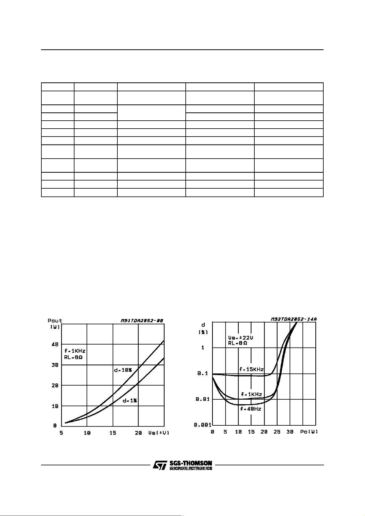
Figure 1: OutputPower vs. Supply Voltage
4/13
Figure2: Distortionvs. OutputPower

Figure 3: OutputPower vs. Supply Voltage. Figure4: Distortionvs. OutputPower.
TDA2052
Figure 5: Distortionvs. Frequency.
Figure 7: QuiescentCurrent vs. Supply Voltage
Figure6: Distortionvs. Frequency.
Figure8: SupplyVoltageRejectionvs.Frequency.
5/13

TDA2052
Figure 9: Bandwidth.
Figure 11: TotalPower Dissipation & Efficiency
vs. OutputPower.
Figure10: OutputAttenuation& QuiescentCur-
rent vs. V
pin3
.
Figure12: TotalPowerDissipation& Efficiency
vs. Output Power.
6/13

Figure 13: P.C.Board andComponents Layoutof the Circuit of Fig. 14(1:1 scale)
TDA2052
Figure 14: Demo Board Schematic.
7/13

TDA2052
MUTE/STAND-BY FUNCTION
The pin 3 (MUTE/STAND-BY) controls the amplifier status by three different thresholds, referred
to-V
S.
When its voltage is lower than the first threshold
(1V, with a +70mV hysteresis), the amplifier is in
STAND-BY and all the final stage current gener-
Figure 15.
ators are off. Only the input MUTE stage is on in
orderto preventpop-on problems.
At V
=1.8V the final stage current generators
pin3
are switched on and the amplifier operates in
MUTE.
For V
=2.7V the amplifier is definitely on
pin3
(PLAYcondition)
8/13

TDA2052
SHORT-CIRCUIT PROTECTION
The TDA 2052 has an original circuit which protects the deviceduring accidental short-circuitbetween output and GND / -Vs / +Vs, taking it in
STAND-BY mode, so limiting also dangerousDC
current flowing throught the loudspeaker.
If a short-circuitor an overload dangerousfor the
final transistors are detected,the concernedSOA
circuit sends out a signal to the latching circuit
(with a 10µs delay time that prevents fast random
spikes from inadvertently shutting the amplifier
off) which makes Q
Diagram). Q
immediatelyshort-circuits to ground
1
and Q2saturate (see Block
1
the A point turning the final stage off while Q
short-circuits to ground the external capacitor
driving the pin 3 (Mute/Stand-by) towards zero
potential.
Only when the pin 3 voltage becomes lower than
1V, the latching circuit is allowed to reset itself
and restart the amplifier, provided that the shortcircuit condition has been removed. In fact, a window comparator is present at the output and it is
aimed at preventingthe amplifierfrom restartingif
the output voltageis lower than0.35 Total Supply
Voltage or higher than 0.65 Total Supply Voltage.
If the output voltage lies between these two
thresholds, one may reasonably suppose the
short-circuit has been removed and the amplifier
may start operatingagain.
The PLAY/MUTE/STAND-BY function pin (pin 3)
is both ground- and positive supply-compatible
and can be interfacedby means of the R
5,C3
net
either to a TTL or CMOS output (µ-Processor) or
to a specificapplication circuit.
The R
net is fundamental,because connect-
5,C3
ing this pin directly to a low output impedance
driver such as TTL gate would preventthe correct
operation during a short-circuit. Actually a final
stage overload turns on the protection latching
circuit that makesQ
try to drive the pin 3 voltage
2
under 0.8 V. Since the maximum current this pin
can stand is 3 mA, one must make sure the following condition is met:
THERMAL PROTECTION
The thermal protection operates on the 125µA
current generator, linearly decreasing its value
from 90°C on. By doing this, the A voltage slowly
decreases thus switching the amplifier first to
MUTE (at 145°C) and then to STAND-BY
(155°C).
Figure16: ThermalProtectionBlock Diagram
2
The maximum allowable power dissipation depends on the size of the external heatsink (thermal resistance case-ambient); figure 17 shows
the dissipable power as a function of ambient
temperaturefor different thermal resistance.
Figure17: MaximumAllowable PowerDissipa-
tion vs. AmbientTemperature.
(VA− 0.7V)
≥
R
that yields: R
5
5, min
3mA
= 1.5KΩwithVA=5V.
In order to prevent pop-on and -off transients,it is
advisable to calculate the C
,R5net in such a
3
way that the STAND-BY/MUTEand MUTE/PLAY
threshold crossing slope (positive at the turn-on
and vice-versa)is less than 100 V/sec.
9/13

TDA2052
APPLICATION NOTES
90W MULTIWAY SPEAKER SYSTEM
The schematic diagram of figure 18, shows the
solution that we have closen as a suggestion for
Hi-Fiand especiallyTV applications.
The multiway system provides the separation of
the musical signal not only for the loudspeakers,
but also for the power amplifierswith the following
advantages:
Figure 18: MultiwayApplicationCircuit
- reduced power level required of each individual amplifier
- complete separation of the ways (if an amplifier is affected by clipping distortion, the others are not)
- protection of tweeters (the high power harmonics generated by low frequency clipping
can not damagethe delicate tweeters that are
drivenby independentpower amplifier)
- highpower dedicatedto low frequencies
10/13

TDA2052
As shown in Figure 19, the R-C passive network
for low-pass and High-pass give a cut with a
slope of 12dB/octave
A further advantage of thisapplication is that connecting each speaker direcly to its amplifier, the
musical signal is not modified by the variations of
the impedance of thecrossover over frequency.
The subwoofer is designed for obtaining high
sound pressure level with low distortion without
stereo effect.
In the application of figure 18, the subwoofer
plays the 20 to 300 Hzfrequency range,while the
remaining 300 Hz to 20KHz are sentto two separate channels withstereo effect.
The multiway system makes use of three
TDA2052, one for driving the subwoofer with
OUT higherthan 40W (THD = 10%), 28W undis-
P
torted (THD = 0.01%), while the others two
TDA2052 are used for driving the mid/high frequency speakers of L/R channels, delivering
OUT = 25W (THD = 10%) and 20W @ THD =
P
0.01%
Figure 20: Distortionvs OutputPower
(Subwoofer)
Figure19: FrequencyResponse
Figure21:Distortionvs Output Power
(Midrange/Tweeter)
11/13

TDA2052
HEPTAWATT PACKAGEMECHANICAL DATA
DIM.
MIN. TYP. MAX. MIN. TYP. MAX.
A 4.8 0.189
C 1.37 0.054
D 2.4 2.8 0.094 0.110
D1 1.2 1.35 0.047 0.053
E 0.35 0.55 0.014 0.022
F 0.6 0.8 0.024 0.031
F1 0.9 0.035
G 2.41 2.54 2.67 0.095 0.100 0.105
G1 4.91 5.08 5.21 0.193 0.200 0.205
G2 7.49 7.62 7.8 0.295 0.300 0.307
H2 10.4 0.409
H3 10.05 10.4 0.396 0.409
L 16.97 0.668
L1 14.92 0.587
L2 21.54 0.848
L3 22.62 0.891
L5 2.6 3 0.102 0.118
L6 15.1 15.8 0.594 0.622
L7 6 6.6 0.236 0.260
M 2.8 0.110
M1 5.08 0.200
Dia 3.65 3.85 0.144 0.152
mm inch
12/13

TDA2052
Information furnished is believed to be accurate and reliable.However, SGS-THOMSON Microelectronics assumes no responsibility for the
consequences of use of such information nor for any infringement of patents or other rights of third partieswhich may result from its use. No
license is granted by implicationor otherwise under any patentor patentrights of SGS-THOMSON Microelectronics. Specificationmentioned
in this publication are subject to change without notice. This publication supersedes and replaces all information previously supplied. SGSTHOMSON Microelectronics products are not authorizedfor use as critical components in life support devices or systems without express
written approval of SGS-THOMSON Microelectronics.
1997 SGS-THOMSON Microelectronics – Printedin Italy – All Rights Reserved
HEPTAWATT is a Trademark of the SGS-THOMSON Microelectronics
SGS-THOMSON Microelectronics GROUPOF COMPANIES
Australia - Brazil - Canada- China - France - Germany -HongKong - Italy - Japan - Korea - Malaysia - Malta- Morocco - The Netherlands-
Singapore - Spain - Sweden - Switzerland- Taiwan - Thailand- United Kingdom - U.S.A.
13/13
 Loading...