


STPS30L120C
Power Schottky rectifier
Features
■ High junction temperature capability
■ Avalanche capability specified
■ Low forward voltage drop current
■ High frequency operation
■ Insulated package: TO-220FPAB
– Insulating voltage = 1500 V rms
– Typical package capacitance 12 pF
Description
This dual center tap Schottky rectifier is suited for
high frequency switch mode power supplies.
Packaged in TO-220AB, I
this device provides adaptor designers with an
optimized price-performance ratio.
Figure 1. Electrical characteristics
V
I
2
PAK and TO-220FPAB,
I
"Forward"
2 x I
O
(a)
X
A1
A2
K
A2
K
A1
TO-220AB
STPS30L120CT
A1
2
PAK
I
STPS30L120CR
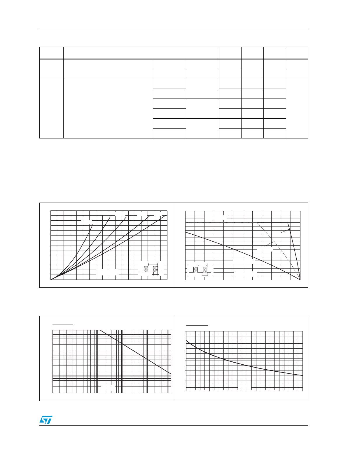
Table 1. Device summary
Symbol Value
K
K
A1
TO-220FPAB
STPS30L120CFP
A2
K
A2
I
I
F
I
V
RRM
V
V
R
AR
"Reverse"
a. V
and I
ARM
operating area defined in Figure 13. V
must respect the reverse safe
ARM
pulse measurements (t
are static characteristics.
O
< 1 µs). VR, IR, V
p
X
I
R
V
V
To
I
AR
F(Io)
V
AR
V
V
F(2xIo)
F
and IAR are
and VF,
RRM
2 x 15 A
F(AV)
120 V
V
RRM
T
j(max)
0.51 V
V
F(typ)
150 °C
May 2011 Doc ID 16313 Rev 3 1/10
www.st.com
10

Characteristics STPS30L120C
1 Characteristics
Table 2. Absolute ratings (limiting values, per diode)
Symbol Parameter Value Unit
V
I
F(RMS)
I
F(AV)
I
FSM
P
V
ARM
V
ASM
T
1. Refer to Figure 13
2. condition to avoid thermal runaway for a diode on its own heatsink
Table 3. Thermal parameters
Repetitive peak reverse voltage 120 V
RRM
Forward rms current 30 A
Average forward
current, δ = 0.5
Surge non repetitive
forward current
Repetitive peak
ARM
avalanche power
Maximum repetitive
(1)
peak avalanche voltage
Maximum single pulse
(1)
peak avalanche voltage
Storage temperature range -65 to + 175 °C
stg
T
Maximum operating junction temperature
j
<
Rth(j-a)
1
dPtot
dTj
Total package 30 A
t
= 10 ms sinusoidal 220 A
p
= 1 µs, Tj = 25 °C 11500 W
t
p
= 1 µs, Tj < 150 °C, IAR < 23 A 150 V
t
p
t
= 1 µs, Tj < 150 °C, IAR < 23 A 150 V
p
(2)
150 °C
Symbol Parameter Value Unit
R
R
th(j-c)
th(c)
Junction to case
Coupling
TO-220AB, I
TO-220FPAB
TO-220AB, I
2
2
PA K
PA K
Per diod e
To ta l
Per diod e
To ta l
To ta l
TO-220FPAB 3
1.3
0.7
4.5
3.8
0.1
°C/W
When the diodes 1 and 2 are used simultaneously :
T
(diode 1) = P(diode 1) x R
j
(per diode) + P(diode 2) x R
th(j-c)
th(c)
2/10 Doc ID 16313 Rev 3
STPS30L120C Characteristics
Table 4. Static electrical characteristics (per diode)
Symbol Test conditions Min. Typ. Max. Unit
T
= 25 °C
(1)
I
R
V
Reverse leakage current
(2)
Forward voltage drop
F
j
T
= 125 °C - 12 35 mA
j
T
= 25 °C
j
= 125 °C - 0.51 0.57
T
j
T
= 25 °C
j
= 125 °C - 0.65 0.71
T
j
= 25 °C
T
j
T
= 125 °C - 0.755 0.84
j
= V
V
R
= 5 A
I
F
= 15 A
I
F
= 30 A
I
F
RRM
--200µA
- - 0.675
- - 0.88
- - 1.08
1. Pulse test : tp = 5 ms, δ < 2%
2. Pulse test : t
= 380 µs, δ < 2%
p
To evaluate the maximum conduction losses use the following equation :
P = 0.58 x I
Figure 2. Average forward power dissipation
P (W)
F(AV)
14
12
10
8
6
4
2
0
0 2 4 6 8 10 12 14 16 18
Figure 4. Normalized avalanche power
+ 0.0087 I
F(AV)
F2(RMS)
versus average forward current
(per diode)
δ=0.1
δ=0.2
δ=0.05
I (A)
F(AV)
δ=0.5
δ
=tp/T
derating versus pulse duration
Figure 3. Average forward current versus
ambient temperature
(
δ = 0.5, per diode)
I (A)
F(AV)
δ=1
T
tp
18
R
T
th(j-a)=Rth(j-c)
tp
R
=15°C/W
th(j-a)
T (°C)
amb
TO-220AB
TO-220FP
16
14
12
10
8
6
4
2
=tp/T
δ
0
0 25 50 75 100 125 150
Figure 5. Normalized avalanche power
derating versus junction
temperature
P(tp)
1
0.1
0.01
0.001
ARM
P (1 µs)
ARM
0.10.01 1
t (µs)
p
10 100 1000
P(Tj)
ARM
P (25 °C)
ARM
1.2
1
0.8
0.6
0.4
0.2
0
25 50 75 100 125 150
T (°C)
j
V
Doc ID 16313 Rev 3 3/10
 Loading...