

Features
■ High junction temperature capability
■ Avalanche rated
■ Low leakage current
■ Good trade-off between leakage current and
forward voltage drop
■ High frequency operation
■ AEC-Q 101 qualified
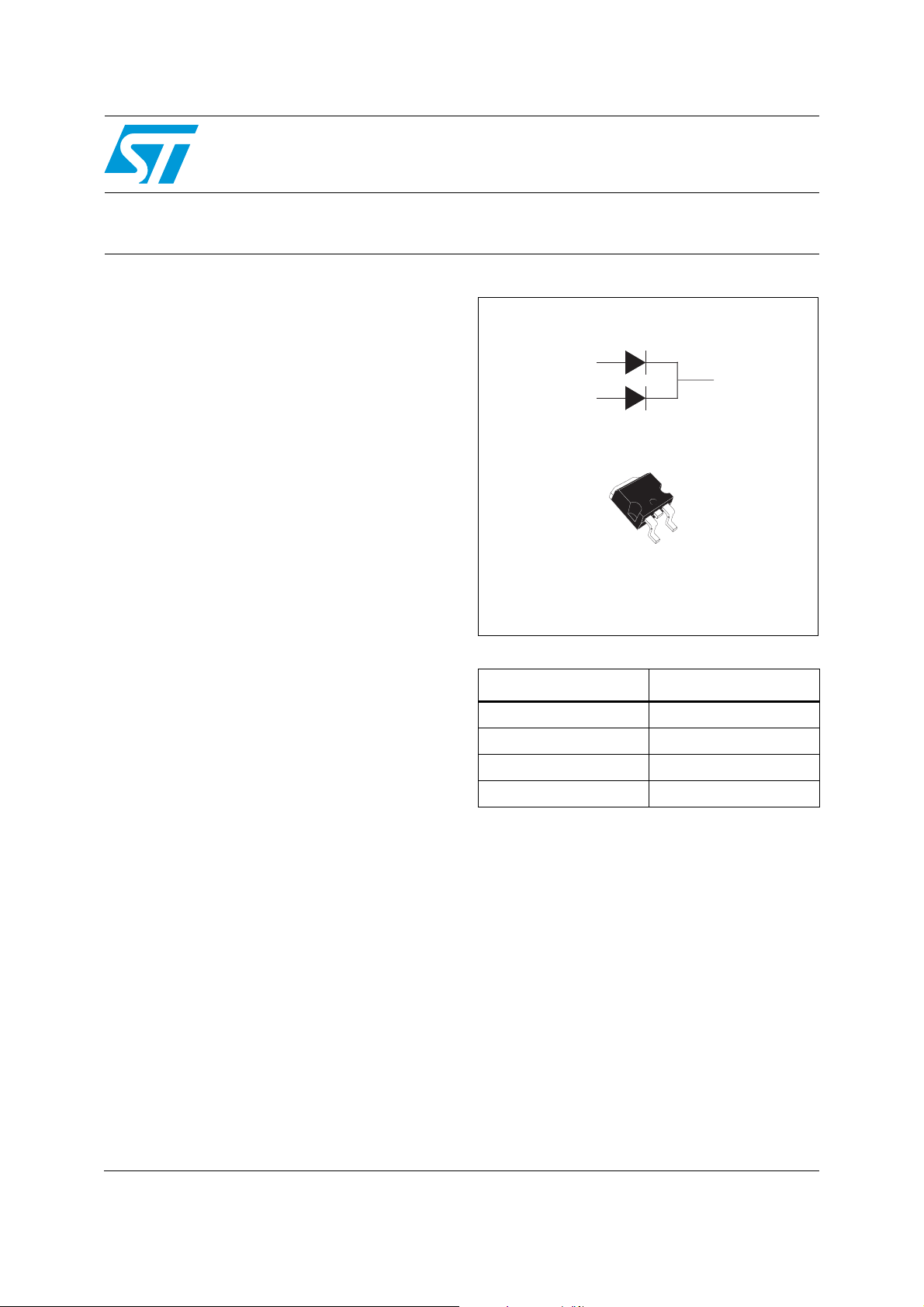
STPS30H60-Y
Automotive power Schottky rectifier
Datasheet − production data
A1
K
A2
K
Description
Dual centre tab Schottky rectifier suited for high
frequency switch mode power supply.
Packaged in D
use in automotive applications. In these
applications this device provides a good margin
between the remaining voltage applied on the
diode and the voltage capability of the diode.
2
PAK, this device is designed for
A2
A1
D2PAK
STPS30H60CGY-TR
Table 1. Device summary
Symbol Value
I
F(AV)
V
RRM
T
j
V
F (typ)
2 X 15 A
60 V
175 °C
0.535 V
March 2012 Doc ID 022824 Rev 1 1/7
This is information on a product in full production.
www.st.com
7

Characteristics STPS30H60-Y
1 Characteristics
Table 2. Absolute ratings (limiting values per diode)
Symbol Parameter Value Unit
V
I
F(RMS)
I
F(AV)
I
P
T
1. condition to avoid thermal runaway for a diode on its own heatsink
Table 3. Thermal parameters
Repetitive peak reverse voltage 60 V
RRM
Forward rms current 30 A
Average forward current, δ = 0.5 Tc = 155 °C
Surge non repetitive forward current tp = 10 ms sinusoidal 230 A
FSM
Relative peak avalanche power Tj = 125 °C tp = 10 µs 715 W
ARM
Operating junction temperature range
T
j
Storage temperature range -65 to + 175 °C
stg
dPtot
dTj
<
Rth(j-a)
1
(1)
Per diode 15
Total package 30
-40 to + 175 °C
Symbol Parameter Value Unit
R
R
Table 4. Static electrical characteristics
Junction to case
th(j-c)
Coupling 0.1
th(c)
Per diode 1.5
°C/WTotal 0.8
Symbol Parameter Test conditions Min. Typ. Max. Unit
(1)
I
V
1. Pulse test: tp = 5 ms, δ < 2%
2. Pulse test: t
Reverse leakage current
R
(2)
Forward voltage drop
F
= 380 µs, δ < 2%
p
= 25 °C
T
j
= 125 °C 8 25
T
j
T
= 25 °C
j
= 125 °C 435 470
T
j
= 25 °C
T
j
= 125 °C 535 570
T
j
= 25 °C
T
j
= 125 °C 635 690
T
j
V
= V
R
I
= 7.5 A
F
I
= 15 A
F
I
= 30 A
F
RRM
60 µA
550
660
820
A
mA
mV
To evaluate the conduction losses use the following equation:
P = 0.45 x I
2/7 Doc ID 022824 Rev 1
+ 0.008 x I
F(AV)
F2(RMS)
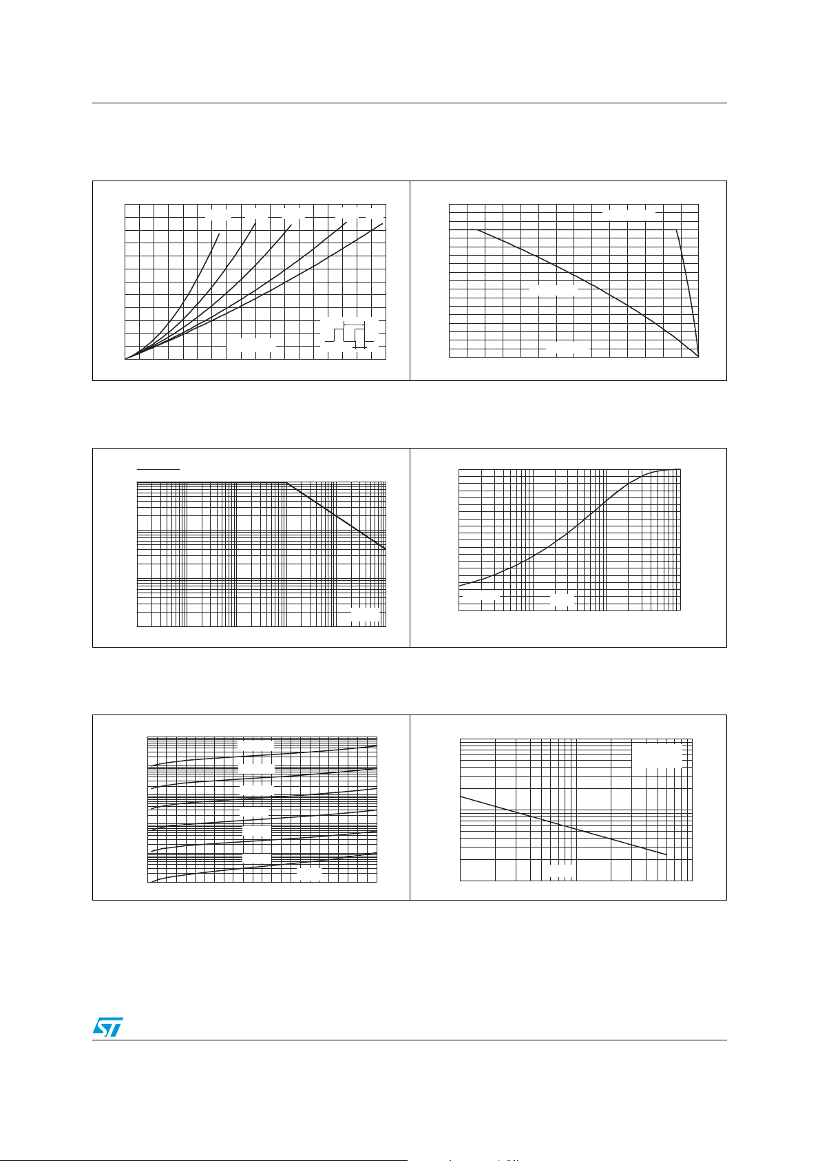
STPS30H60-Y Characteristics
Figure 1. Conduction losses versus
average forward current
P (W)
F(AV)
12
10
8
6
4
2
0
0 2 4 6 8 10 12 14 16 18
δ=0.05
δ=0.1 δ=0.2
I (A)
F(AV)
δ
δ=0.5
T
=tp/T
Figure 3. Normalized avalanche power
derating versus pulse duration
P(tp)
ARM
P (1 µs)
ARM
1
0.1
0.01
0.001
0.10.01 1
10 100 1000
t (µs)
Figure 2. Average forward current versus
ambient temperature
(δ = 0.5, per diode)
I (A)
F(AV)
δ=1
tp
18
16
14
12
10
8
6
4
2
0
0 25 50 75 100 125 150 175
R
th(j-a)
=15 °C/W
T (°C)
amb
R
th(j-a)=Rth(j-c)
Figure 4. Relative variation of thermal
impedance junction to case versus
pulse duration
Z/R
th(j-c) th(j-c)
1.0
0.9
0.8
0.7
0.6
0.5
0.4
0.3
0.2
Single pulse
0.1
p
0.0
1.E-03 1.E-02 1.E-01 1.E+00
t (s)
p
Figure 5. Reverse leakage current versus
reverse voltage applied
(typical values, per diode)
I (mA)
R
1.E+02
1.E+01
1.E+00
1.E-01
1.E-02
1.E-03
0 5 10 15 20 25 30 35 40 45 50 55 60
Tj=150°C
Tj=125°C
Tj=100°C
Tj=75°C
Tj=50°C
Tj=25°C
V (V)
R
Doc ID 022824 Rev 1 3/7
Figure 6. Junction capacitance versus
reverse voltage applied
(typical values, per diode)
C(nF)
10.0
1.0
V (V)
0.1
1 10 100
R
V
osc
F=1MHz
=30mV
Tj=25°C
RMS
 Loading...