

STPS30120C
Power Schottky rectifier
Features
■ High junction temperature capability
■ Avalanche rated
■ Low leakage current
■ Good trade-off between leakage current and
forward voltage drop
Description
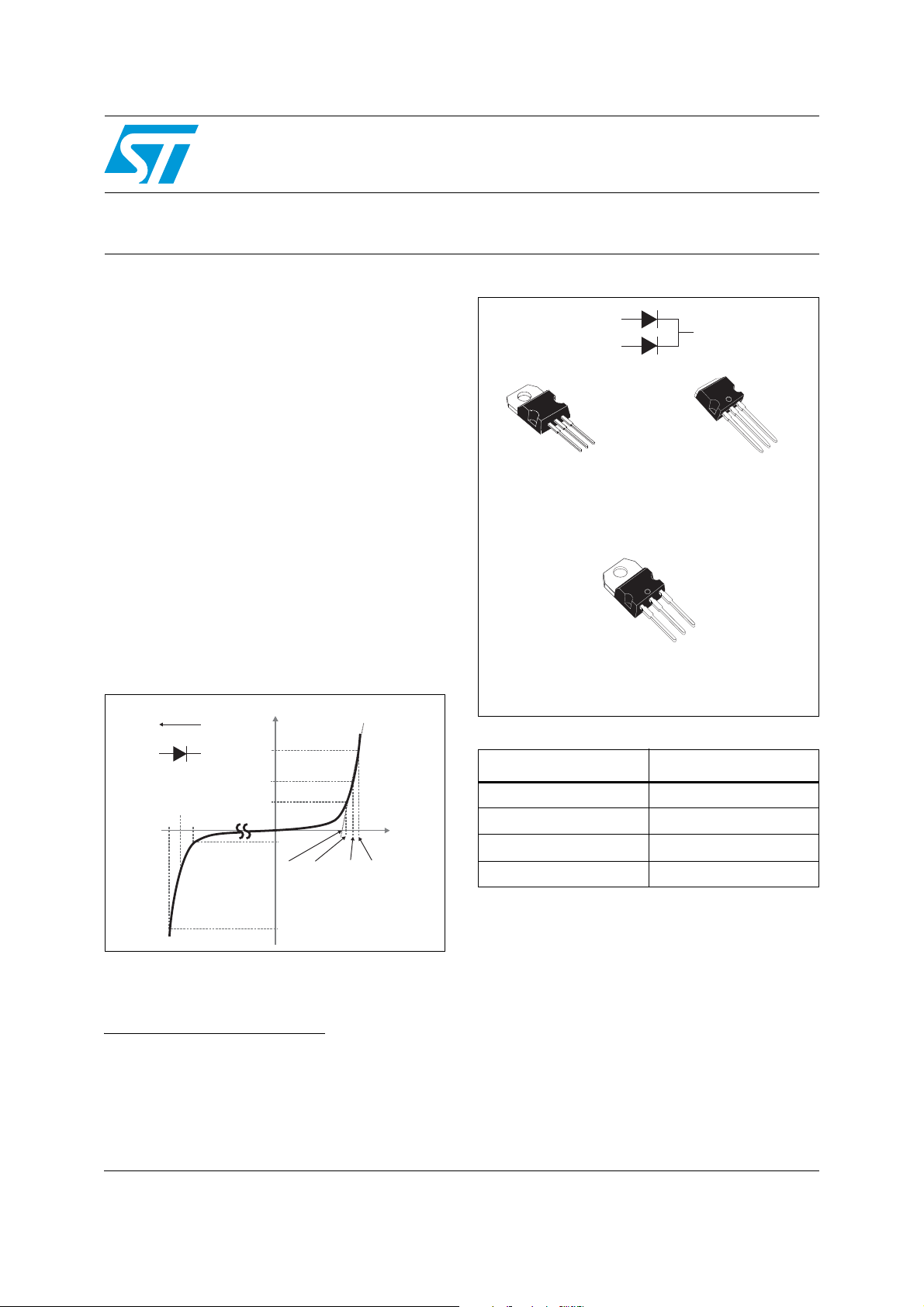
Dual center tap Schottky rectifier suited for high
frequency switch mode power supply.
Packaged in TO-220AB, TO-220AB narrow leads,
2
and I
PAK, this device is intended to be used in
notebook and LCD adaptors, desktop SMPS,
providing in these applications a margin between
the remaining voltages applied on the diode and
the voltage capability of the diode.
Figure 1. Electrical characteristics
2 x I
I
"Forward"
O
I
F
I
O
I
R
V
V
F(Io)
To
V
I
V
RRM
V
V
R
AR
"Reverse"
(a)
X
X
V
V
V
F(2xIo)
F
A1
A2
K
A2
K
A1
TO-220AB
STPS30120CT
K
A1
TO-220AB narrow leads
STPS30120CTN
Table 1. Device summary
Symbol Value
I
2 x 15 A
F(AV)
120 V
V
RRM
T
j(max)
0.57 V
V
F(typ)
K
K
A1
2
I
PA K
STPS30120CR
A2
K
175 °C
A2
K
I
AR
a. V
ARM
and I
must respect the reverse safe
ARM
operating area defined in Figure 10. V
pulse measurements (t
are static characteristics.
< 1 µs). VR, IR, V
p
and IAR are
AR
and VF,
RRM
January 2012 Doc ID 11213 Rev 4 1/9
www.st.com
9
Characteristics STPS30120C
1 Characteristics
Table 2. Absolute ratings (limiting values, per diode)
Symbol Parameter Value Unit
V
I
F(RMS)
I
F(AV)
I
FSM
P
V
ARM
V
ASM
T
1. Refer to Figure 10
2. condition to avoid thermal runaway for a diode on its own heatsink
Table 3. Thermal parameters
Repetitive peak reverse voltage 120 V
RRM
Forward rms current 30 A
Average forward
current
δ = 0.5
= 145 °C
T
c
Per diode
Per device
Surge non repetitive forward current tp = 10 ms sinusoidal 180 A
Repetitive peak avalanche power tp = 1 µs Tj = 25 °C 6700 W
ARM
Maximum repetitive
(1)
peak avalanche voltage
Maximum single pulse
(1)
peak avalanche voltage
Storage temperature range -65 to + 175 °C
stg
T
Maximum operating junction temperature
j
<
Rth(j-a)
1
dPtot
dTj
= 1 µs, Tj < 150 °C, IAR < 13.4 A 150 V
t
p
= 1 µs, Tj < 150 °C, IAR < 13.4 A 150 V
t
p
(2)
15
30
175 °C
Symbol Parameter Value Unit
R
R
th(j-c)
th(c)
Junction to case
Per diode
To ta l
Coupling Total 0.3 °C/W
2.2
1.3
°C/W
A
When the diodes 1 and 2 are used simultaneously :
T
(diode 1) = P(diode 1) x R
j
2/9 Doc ID 11213 Rev 4
(per diode) + P(diode 2) x R
th(j-c)
th(c)
STPS30120C Characteristics
Table 4. Static electrical characteristics (per diode)
Symbol Test conditions Min. Typ. Max. Unit
(1)
I
R
V
Reverse leakage current
(2)
Forward voltage drop
F
Tj = 25 °C
VR = V
= 125 °C 2.5 7.5 mA
T
j
T
= 25 °C
j
= 125 °C 0.57 0.61
T
j
= 25 °C
T
j
Tj = 125 °C 0.7 0.74
T
= 25 °C
j
= 125 °C 0.83 0.89
T
j
RRM
= 5 A
I
F
= 15 A
I
F
IF = 30 A
1. Pulse test : tp = 5 ms, δ < 2%
2. Pulse test : tp = 380 μs, δ < 2%
To evaluate the maximum conduction losses use the following equation :
P = 0.59 x I
Figure 2. Average forward power
P (W)
F(AV)
15
14
13
12
11
10
9
8
7
6
5
4
3
2
1
0
0 2 4 6 8 10 12 14 16 18
Figure 4. Normalized avalanche power
+ 0.01 I
F(AV)
F2(RMS)
dissipation versus average forward
current (per diode)
δ = 0.2
δ = 0.1
δ = 0.05
I (A)
F(AV)
δ = 0.5
δ
=tp/T
δ = 1
T
tp
derating versus pulse duration
Figure 3. Average forward current versus
ambient temperature
(
δ = 0.5, per diode)
I (A)
F(AV)
18
16
14
12
10
8
6
δ
=tp/T
T
tp
4
2
0
0 25 50 75 100 125 150 175
Figure 5. Normalized avalanche power
derating versus junction
temperature
P(tp)
P (1µs)
ARM
1
ARM
P (25 °C)
1.2
1
P(T)
ARM j
ARM
R=R
th(j-a) th(j-c)
R =15°C/W
th(j-a)
T (°C)
amb
15 µA
0.74
0.92
V
1.02
0.1
0.01
0.001
0.10.01 1
10 100
0.8
0.6
0.4
0.2
T (°C)
t (µs)
p
1000
0
25 50 75 100 125
j
150
Doc ID 11213 Rev 4 3/9

Characteristics STPS30120C
Figure 6. Relative variation of thermal
impedance junction to ambient
versus pulse duration
Z/R
th(j-c) th(j-c)
1.0
0.9
0.8
0.7
0.6
0.5
0.4
0.3
0.2
Single pulse
0.1
0.0
1.E-03 1.E-02 1.E-01 1.E+00
t (s)
p
δ
T
=tp/T
Figure 8. Junction capacitance versus
reverse voltage applied
(typical values, per diode)
C(pF)
1000
100
F=1MHz
V =30mV
OSC RMS
T =25°C
j
Figure 7. Reverse leakage current versus
reverse voltage applied
(typical values, per diode)
I (mA)
R
1.E+02
1.E+01
1.E+00
1.E-01
1.E-02
1.E-03
tp
1.E-04
1.E-05
0 10 20 30 40 50 60 70 80 90 100 110 120
T=150°C
j
T=125°C
j
T=100°C
j
T=75°C
j
T=50°C
j
T=25°C
j
V (V)
R
Figure 9. Forward voltage drop versus
forward current (per diode)
I (A)
FM
100
T=125°C
j
(maximum values)
T=125°C
j
(typical values)
10
T=25°C
j
(maximum values)
V (V)
10
1 10 100
R
1
0.0 0.2 0.4 0.6 0.8 1.0 1.2 1.4 1.6
Figure 10. Reverse safe operating area (tp < 1 µs and Tj < 150 °C)
I (A)
arm
18
17
16
15
14
13
12
V (V)
11
120
130
140
arm
150
160
170
V (V)
FM
4/9 Doc ID 11213 Rev 4

STPS30120C Package information
2 Package information
● Epoxy meets UL94, V0
● Cooling method: by conduction (C)
● Recommended torque value: 0.4 to 0.6 N·m
In order to meet environmental requirements, ST offers these devices in different grades of
ECOPACK
specifications, grade definitions and product status are available at: www.st.com
ECOPACK
Table 5. TO-220AB dimensions
®
packages, depending on their level of environmental compliance. ECOPACK®
®
is an ST trademark.
.
Dimensions
Ref.
Millimeters Inches
Min. Max. Min. Max.
A 4.40 4.60 0.173 0.181
H2
Dia
A
C
C 1.23 1.32 0.048 0.051
D 2.40 2.72 0.094 0.107
E 0.49 0.70 0.019 0.027
L2
F2
F1
L5
L6
L9
L4
F
G1
L7
F 0.61 0.88 0.024 0.034
F1 1.14 1.70 0.044 0.066
F2 1.14 1.70 0.044 0.066
G 4.95 5.15 0.194 0.202
D
G1 2.40 2.70 0.094 0.106
H2 10 10.40 0.393 0.409
L2 16.4 typ. 0.645 typ.
M
E
L4 13 14 0.511 0.551
L5 2.65 2.95 0.104 0.116
G
L6 15.25 15.75 0.600 0.620
L7 6.20 6.60 0.244 0.259
L9 3.50 3.93 0.137 0.154
M 2.6 typ. 0.102 typ.
Diam. 3.75 3.85 0.147 0.151
Doc ID 11213 Rev 4 5/9

Package information STPS30120C
Table 6. TO-220AB narrow leads dimensions
Dimensions
L20
b1(x3)
1
E
23
e
e1
L1
b (x3)
Ref.
Millimeters Inches
Min. Typ. Max. Min. Typ. Max.
A 4.40 4.60 0.17 0.18
b 0.61 0.88 0.024 0.034
P
Q
D
L30
L
A
F
H1
D1
J1
b1 0.95 1.20 0.037 0.047
c 0.48 0.70 0.019 0.027
D 15.25 15.75 0.60 0.62
D1 1.27 0.05
E 10.00 10.40 0.39 0.41
e 2.40 2.70 0.094 0.106
e1 4.95 5.15 0.19 0.20
F 1.23 1.32 0.048 0.052
H1 6.20 6.60 0.24 0.26
C
J1 2.40 2.72 0.095 0.107
L 13.00 14.00 0.51 0.55
L1 2.60 2.90 0.102 0.114
L20 15.40 0.61
L30 28.90 1.14
∅P 3.75 3.85 0.147 0.151
Q 2.65 2.95 0.104 0.116
6/9 Doc ID 11213 Rev 4

STPS30120C Package information
Devices in I2PAK with nickel-plated back frame must NOT be mounted by frame soldering
like SMDs. Such devices are intended to be through-hole mounted ONLY and in no
circumstances shall ST be held liable for any lack of performance or damage arising out of
soldering of nickel-plated back frames.
Table 7. I2PAK dimensions
Dimensions
Ref.
Millimeters Inches
Min. Max. Min. Max.
A 4.40 4.60 0.173 0.181
A1 2.40 2.72 0.094 0.107
b 0.61 0.88 0.024 0.035
L2
A
E
c2
b1 1.14 1.70 0.044 0.067
D
c 0.49 0.70 0.019 0.028
c2 1.23 1.32 0.048 0.052
L1
L
b1
A1
D 8.95 9.35 0.352 0.368
e 2.40 2.70 0.094 0.106
e1 4.95 5.15 0.195 0.203
b
e
e1
c
E 10 10.40 0.394 0.409
L 13 14 0.512 0.551
L1 3.50 3.93 0.138 0.155
L2 1.27 1.40 0.050 0.055
Doc ID 11213 Rev 4 7/9

Ordering information STPS30120C
3 Ordering information
Table 8. Ordering information
Order code Marking Package Weight Base qty Delivery mode
STPS30120CT STPS30120CT TO-220AB 2.23 g 50 Tube
STPS30120CR STPS30120CR I2PAK 1.49 g 50 Tube
STPS30120CTN STPS30120CTN
TO-220AB
narrow leads
1.9 g 50 Tube
4 Revision history
Table 9. Document revision history
Date Revision Changes
18-Feb-2005 1 First issue.
23-Nov-2006 2 Reformatted to current standards. Added I2PA K p a c k a g e .
17-Feb-2010 3 Updated Ta bl e 2 . Added Figure 1 and Figure 10.
13-Jan-2012 4 Added TO-220AB narrow leads package.
8/9 Doc ID 11213 Rev 4

STPS30120C
Please Read Carefully:
Information in this document is provided solely in connection with ST products. STMicroelectronics NV and its subsidiaries (“ST”) reserve the
right to make changes, corrections, modifications or improvements, to this document, and the products and services described herein at any
time, without notice.
All ST products are sold pursuant to ST’s terms and conditions of sale.
Purchasers are solely responsible for the choice, selection and use of the ST products and services described herein, and ST assumes no
liability whatsoever relating to the choice, selection or use of the ST products and services described herein.
No license, express or implied, by estoppel or otherwise, to any intellectual property rights is granted under this document. If any part of this
document refers to any third party products or services it shall not be deemed a license grant by ST for the use of such third party products
or services, or any intellectual property contained therein or considered as a warranty covering the use in any manner whatsoever of such
third party products or services or any intellectual property contained therein.
UNLESS OTHERWISE SET FORTH IN ST’S TERMS AND CONDITIONS OF SALE ST DISCLAIMS ANY EXPRESS OR IMPLIED
WARRANTY WITH RESPECT TO THE USE AND/OR SALE OF ST PRODUCTS INCLUDING WITHOUT LIMITATION IMPLIED
WARRANTIES OF MERCHANTABILITY, FITNESS FOR A PARTICULAR PURPOSE (AND THEIR EQUIVALENTS UNDER THE LAWS
OF ANY JURISDICTION), OR INFRINGEMENT OF ANY PATENT, COPYRIGHT OR OTHER INTELLECTUAL PROPERTY RIGHT.
UNLESS EXPRESSLY APPROVED IN WRITING BY TWO AUTHORIZED ST REPRESENTATIVES, ST PRODUCTS ARE NOT
RECOMMENDED, AUTHORIZED OR WARRANTED FOR USE IN MILITARY, AIR CRAFT, SPACE, LIFE SAVING, OR LIFE SUSTAINING
APPLICATIONS, NOR IN PRODUCTS OR SYSTEMS WHERE FAILURE OR MALFUNCTION MAY RESULT IN PERSONAL INJURY,
DEATH, OR SEVERE PROPERTY OR ENVIRONMENTAL DAMAGE. ST PRODUCTS WHICH ARE NOT SPECIFIED AS "AUTOMOTIVE
GRADE" MAY ONLY BE USED IN AUTOMOTIVE APPLICATIONS AT USER’S OWN RISK.
Resale of ST products with provisions different from the statements and/or technical features set forth in this document shall immediately void
any warranty granted by ST for the ST product or service described herein and shall not create or extend in any manner whatsoever, any
liability of ST.
ST and the ST logo are trademarks or registered trademarks of ST in various countries.
Information in this document supersedes and replaces all information previously supplied.
The ST logo is a registered trademark of STMicroelectronics. All other names are the property of their respective owners.
© 2012 STMicroelectronics - All rights reserved
STMicroelectronics group of companies
Australia - Belgium - Brazil - Canada - China - Czech Republic - Finland - France - Germany - Hong Kong - India - Israel - Italy - Japan -
Malaysia - Malta - Morocco - Philippines - Singapore - Spain - Sweden - Switzerland - United Kingdom - United States of America
www.st.com
Doc ID 11213 Rev 4 9/9
 Loading...