

ST STPS24045TV User Manual
®
MAIN PRODUCT CHARACTERISTICS
STPS24045TV
POWER SCHOTTKY RECTIFIER
I
F(AV)
V
RRM
(max) 0.67 V
V
F
2 x 120 A
45 V
FEATURES AND BENEFITS
VERY SMALL CONDUCTION LOSSES
n
NEGLIGIBLE SWITCHING LOSSES
n
EXTREMELY FAST SWITCHING
n
LOW THERMAL RESISTANCE
n
INSULATED PACKAGE:
n
Insulating voltage = 2500 V
(RMS)
Capacitance = 45pF
AVALANCHE CAPABILITY SPECIFIED
n
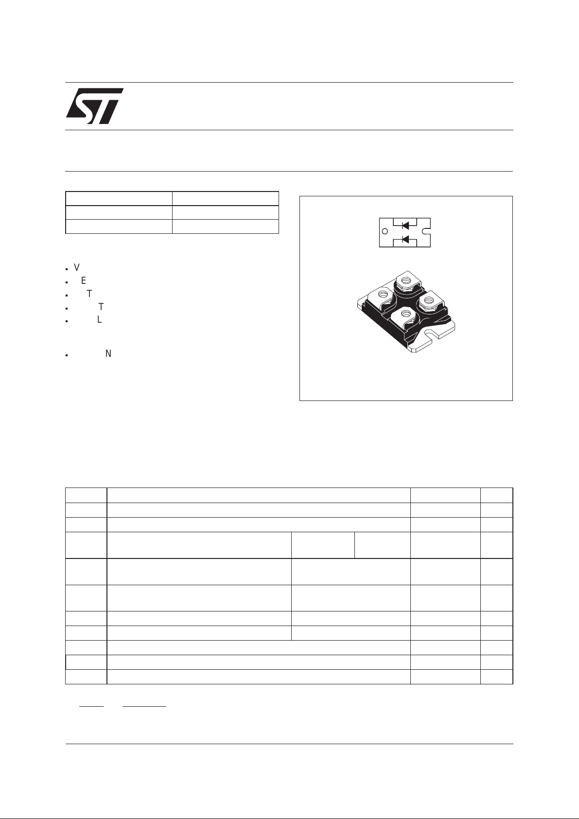
DESCRIPTION
Dual power Schottky rectifier suited for Switched
Mode Power Supplies and high frequency DC to
DC converters.
Packaged in ISOTOP, this device is especially intended for use in low voltage, high frequency inverters, free wheeling and polarity protection
applications.
ABSOLUTE RATINGS (limiting values, per diode)
K2 A2
A1K1
ISOTOP
ISOTOP isatrademark of STMicroelectronics
TM
Symbol Parameter Value Unit
V
RRM
I
F(RMS)
I
F(AV)
I
FSM
Repetitive peak reverse voltage 45 V
RMS forward current 170 A
Average forward current Tc = 80°C
δ = 0.5
Surge non repetitive forward current tp = 10 ms
Per diode
Per device
120
240
1500 A
Sinusoidal
I
RRM
Repetitive peak reverse current tp=2µs
2A
F = 1kHz square
I
RSM
P
ARM
T
stg
Non repetitive peak reverse current tp = 100 µs square 10 A
Repetitive peak avalanche power tp = 1µs Tj = 25°C 43000 W
Storage temperature range - 55 to + 150 °C
Tj Maximum operating junction temperature 150 °C
dV/dt Critical rate of rise of reverse voltage 10000 V/µs
dPtot
*:
<
dTj Rth j a
July 2003 - Ed : 4A
thermal runaway condition for a diode on its own heatsink
−1()
A
1/4
STPS24045TV
THERMAL RESISTANCES
Symbol Parameter Value Unit
R
th (j-c)
R
th (c)
When the diodes 1 and 2 are used simultaneously :
∆ Tj(diode 1) = P(diode) x R
STATIC ELECTRICAL CHARACTERISTICS (per diode)
Symbol Parameter Tests Conditions Min. Typ. Max. Unit
I
R
V
Pulse test : * tp=5ms,δ<2%
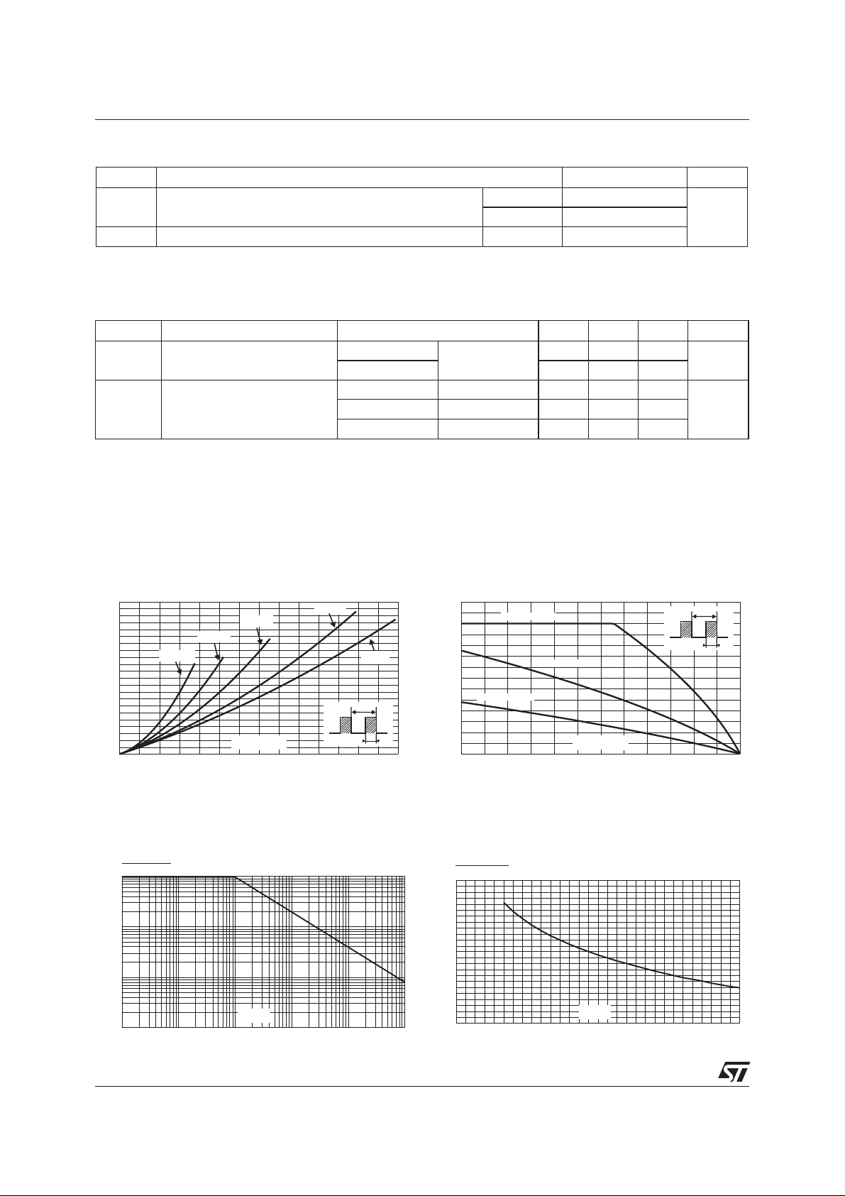
To evaluate the conduction losses use the following equation :
P=0.47xI
Fig. 1: Average forward power dissipation versus
average forward current (per diode).
Junction to case Per diode 0.65 °C/W
Total 0.28
Coupling 0.10
(Per diode) + P(diode 2) x R
th(j-c)
* Reverse leakage current Tj = 25°CV
th(c)
R=VRRM
Tj = 125°C 300
* Forward voltage drop Tj = 25°CI
F
Tj = 125°CI
Tj = 125°CI
** tp = 380 µs, δ <2%
+ 0.00167 x I
F(AV)
F2(RMS)
= 240 A 0.91 V
F
= 240 A 0.72 0.87
F
= 120 A 0.52 0.67
F
Fig. 2: Average forward current versus ambient
temperature (δ= 0.5, per diode).
2mA
PF(av)(W)
110
100
90
80
70
δ = 0.2
δ = 0.1
δ = 0.05
δ = 0.5
δ = 1
60
50
40
30
T
20
10
0
0 20 40 60 80 100 120 140
IF(av) (A)
δ
=tp/T
tp
Fig. 3: Normalized avalanche power derating
versus pulse duration.
P(t)
ARM p
P (1µs)
ARM
1
0.1
0.01
t (µs)
0.001
0.10.01 1
p
10 100 1000
IF(av)(A)
140
120
100
80
60
Rth(j-a)=Rth(j-c)
Rth(j-a)=2°C/W
Rth(j-a)=5°C/W
δ
=tp/T
T
tp
40
20
0
0 25 50 75 100 125 150
Tamb(°C)
Fig. 4: Normalized avalanche power derating
versus junction temperature.
P(t)
ARM p
P (25°C)
ARM
1.2
1
0.8
0.6
0.4
0.2
0
0 25 50 75 100 125 150
T (°C)
j
2/4
 Loading...