

ST STPS20SM60C User Manual
STPS20SM60C
Power Schottky rectifier
Features
■ High current capability
■ Avalanche rated
■ Low forward voltage drop
■ High frequency operation
Description
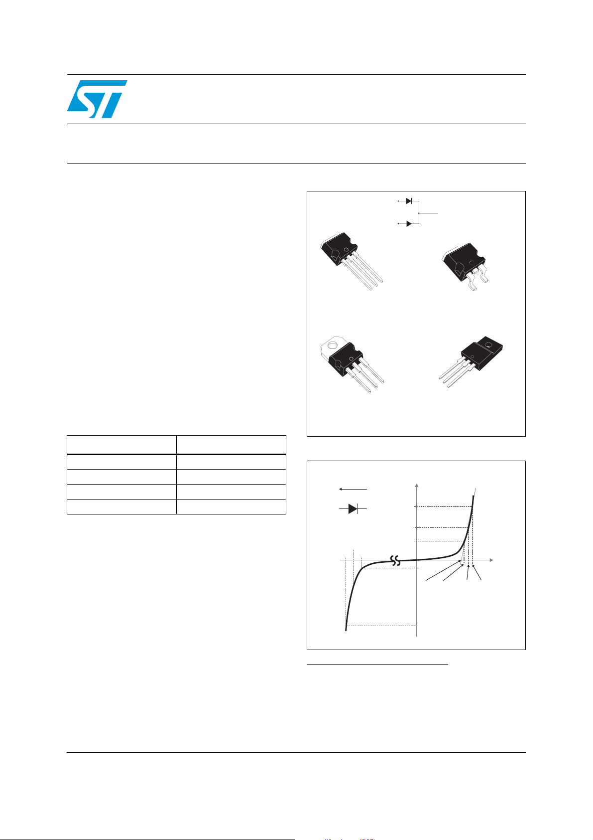
The STPS20SM60C is a dual diode Schottky
rectifier, suited for high frequency switch mode
power supply.
2 x 10 A
60 V
2
PAK and
Packaged in TO-220AB, TO-220FPAB, I
2
D
PAK, this device is intended to be used in
notebook, game station and desktop adapters,
providing in these aplications a good efficiency at
both low and high load.
Table 1. Device summary
Symbol Value
I
F(AV)
V
RRM
(typ) 0.420 V
V
F
(max) 150 °C
T
j
A1
K
A2
K
K
A2
K
A1
I2PAK
STPS20SM60CR
STPS20SM60CG-TR
A1
2
PAK
D
K
A1
K
A2
TO-220FPAB
STPS20SM60CFP
K
A1
TO-220AB
STPS20SM60CT
A2
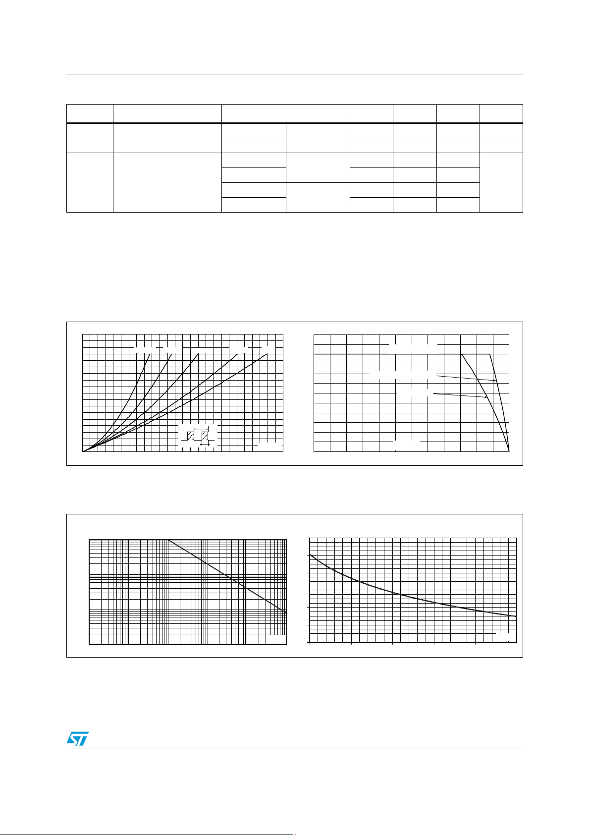
Figure 1. Electrical characteristics
2 x I
O
I
"Forward"
X
V
I
A2
(a)
I
F
I
V
RRM
V
V
a. V
ARM
operating area defined in Figure 14. V
pulse measurements (t
are static characteristics
AR
and I
R
"Reverse"
must respect the reverse safe
ARM
O
< 1 µs). VR, IR, V
p
I
R
V
To
I
AR
V
F(Io)
X
V
V
F(2xIo)
F
and IAR are
AR
and VF,
RRM
V
October 2011 Doc ID 022015 Rev 1 1/11
www.st.com
11

Characteristics STPS20SM60C
1 Characteristics
Table 2. Absolute ratings (limiting values, per diode, at T
otherwise specified)
Symbol Parameter Value Unit
= 25 °C unless
amb
V
I
F(RMS)
I
F(AV)
I
FSM
P
ARM
V
ARM
V
ASM
T
1. For temperature or pulse time duration deratings, please refer to Figure 4 and 5. More details regarding the
avalanche energy measurements and diode validation in the avalanche are provided in the application
notes AN1768 and AN2025.
2. See Figure 14
3. condition to avoid thermal runaway for a diode on its own heatsink
Table 3. Thermal parameters
Repetitive peak reverse voltage 60 V
RRM
Forward rms current 30 A
(3)
T
= 135 °C
c
= 130 °C
T
c
= 110 °C
T
c
= 90 °C
T
c
TO-220AB,
2
PAK, D2PA K
Average forward current,
I
δ = 0.5
TO-220FPAB
Surge non repetitive
forward current
(1)
Repetitive peak avalanche power Tj = 25 °C, tp = 1 µs 8700 W
Maximum repetitive peak
(2)
avalanche voltage
Maximum single pulse
(2)
peak avalanche voltage
Storage temperature range -65 to +175 °C
stg
Maximum operating junction temperature
T
j
<
Rth(j-a)
1
dPtot
dTj
t
= 10 ms sine-wave 220 A
p
< 1 µs, Tj < 150 °C, IAR < 32.6 A 80 V
t
p
t
< 1 µs, Tj < 150 °C, IAR < 32.6 A 80 V
p
Per diode
Per device
Per diode
Per device
10
20
10
20
150 °C
Symbol Parameter Value Unit
per diode 2.00
total 1.13
per diode 4.90
total 4.05
2
PAK , D2PA K 0 .2 5
°C/W
°C/W
R
R
th(j-c)
th(c)
Junction to case
Coupling
TO-220AB
I2PA K , D2PA K
TO-220FPAB
TO-220AB, I
TO-220FPAB 3.20
A
When the two diodes 1 and 2 are used simultaneously:
ΔT
(diode 1) = P(diode 1) x R
j
2/11 Doc ID 022015 Rev 1
(Per diode) + P(diode 2) x R
th(j-c)
th(c)
STPS20SM60C Characteristics
Table 4. Static electrical characteristics (per diode)
Symbol Parameter Test conditions Min. Typ. Max. Unit
(1)
I
R
V
Reverse leakage current
(2)
Forward voltage drop
F
1. Pulse test: tp = 5 ms, δ < 2 %
2. Pulse test: t
= 380 µs, δ < 2 %
p
= 25 °C
T
j
= 125 °C - 5 25 mA
T
j
Tj = 25 °C
= 125 °C - 0.420 0.475
T
j
= 25 °C
T
j
= 125 °C - 0.525 0.600
T
j
V
= V
R
I
= 5 A
F
I
= 10 A
F
RRM
-1040µA
- 0.505 0.545
- 0.580 0.645
To evaluate the conduction losses use the following equation:
P = 0.455 x I
Figure 2. Average forward power dissipation
versus average forward current
(per diode)
P (W)
F(AV)
9
8
7
6
5
4
3
2
1
0
0 1 2 3 4 5 6 7 8 9 10 11 12 13
δ = 0.05
δ = 0.1
Figure 4. Normalized avalanche power
derating versus pulse duration
+ 0.0145 x I
F(AV)
δ = 0.2
T
δ = t / T
p
F2(RMS)
Figure 3. Average forward current versus
ambient temperature
(δ = 0.5, per diode)
I (A)
F(AV)
12
R
δ = 0.5
t
p
δ = 1
I (A)
F(AV)
10
8
6
4
2
0
0 25 50 75 100 125 150
TO-220AB/I PAK/D PAK
= R
th(j-a)
22
TO-220FPAB
T (°C)
amb
th(j-c)
Figure 5. Normalized avalanche power
derating versus junction
temperature
P(tp)
P (1µs)
ARM
1
ARM
P (25 °C)
1.2
1
P(T)
ARM j
ARM
V
0.1
0.01
0.001
0.10.01 1
10 100
0.8
0.6
0.4
0.2
T (°C)
t (µs)
p
1000
0
25 50 75 100 125
j
150
Doc ID 022015 Rev 1 3/11
Characteristics STPS20SM60C
Figure 6. Non repetitive surge peak forward
current versus overload duration
(maximum values, per diode)
I (A)
M
160
140
120
100
80
60
40
I
M
20
0
1.E-03 1.E-02 1.E-01 1.E+00
δ = 0.5
t
TO-220AB/I PAK/D PAK
22
T = 25 °C
c
T = 75 °C
c
T = 125 °C
c
t(s)
Figure 8. Relative thermal impedance
junction to case versus pulse
duration
Z/R
th(j-c) th(j-c)
1.0
0.9
0.8
0.7
0.6
0.5
0.4
0.3
0.2
Single pulse
0.1
0.0
1.E-04 1.E-03 1.E-02 1.E-01 1.E+00
TO-220AB/I PAK/D PAK
22
t (s)
p
Figure 10. Reverse leakage current versus
reverse voltage applied
(typical values, per diode)
I (mA)
R
1.E+02
T = 150 °C
1.E+01
1.E+00
1.E-01
1.E-02
1.E-03
0 102030405060
j
T = 125 °C
j
T = 100 °C
j
T = 75 °C
j
T = 50 °C
j
T = 25 °C
j
V (V)
R
Figure 7. Non repetitive surge peak forward
current versus overload duration
(maximum values, per diode)
I (A)
M
100
90
80
70
60
50
40
30
20
I
M
10
0
1.E-03 1.E-02 1.E-01 1.E+00
δ
= 0.5
t
TO-220FPAB
T = 25 °C
c
T = 75 °C
c
T = 125 °C
c
Figure 9. Relative thermal impedance
junction to case versus pulse
duration
Z/R
th(j-c) th(j-c)
1.0
0.9
0.8
0.7
0.6
0.5
0.4
0.3
Single pulse
0.2
0.1
0.0
1.E-03 1.E-02 1.E-01 1.E+00 1.E+01
TO-220FPAB
t (s)
p
Figure 11. Junction capacitance versus
reverse voltage applied
(typical values, per diode)
C(pF)
1000
100
1 10 100
F = 1 MHz
V = 30 mV
osc RMS
T = 25 °C
j
V (V)
R
4/11 Doc ID 022015 Rev 1
 Loading...