

STPS20S100C
100 V, 20 A power Schottky rectifier
Features
■ High junction temperature capability for
converters located in confined enrironment
■ Low leakage current at high temperature
■ Low static and dynamic losses as a result of the
Schottky barrier
■ Avalanche specification
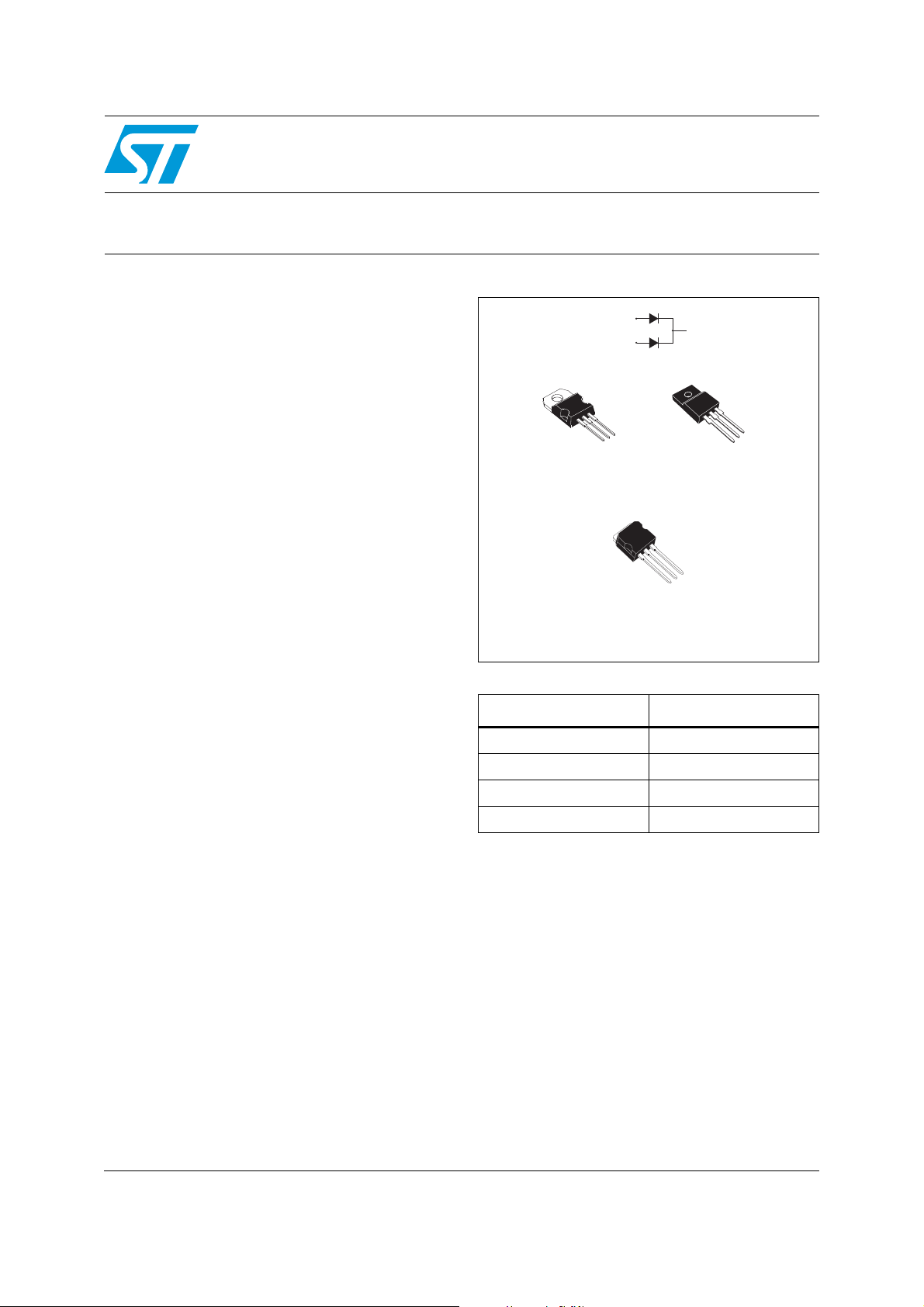
Description
Schottky barrier rectifier designed for high
frequency miniature switched mode power
supplies such as adaptators and on board dc/dc
converters. The device is packaged in TO-220AB,
2
I
PAK and TO-220FPAB.
A1
A2
K
A2
K
A1
TO-220AB
STPS20S100CT
K
TO-220FPAB
STPS20S100CFP
K
A1
I2PAK
STPS20S100CR
Table 1. Device summary
Symbol Value
I
F(AV)
V
RRM
T
j
(max) 0.71 V
V
F
K
A2
A2
K
A1
2 x 10 A
100 V
175 °C
February 2010 Doc ID 11281 Rev 2 1/9
www.st.com
9

Characteristics STPS20S100C
1 Characteristics
Table 2. Absolute ratings (limiting values, per diode)
Symbol Parameter Value Unit
V
I
F(RMS)
I
F(AV)
I
P
T
dV/dt Critical rate of rise of reverse voltage 10000 V/µs
1. condition to avoid thermal runaway for a diode on its own heatsink
Table 3. Thermal resistance
Symbol Parameter Value Unit
Repetitive peak reverse voltage 100 V
RRM
Forward rms current 30 A
2
Average forward
current δ = 0.5
Surge non repetitive forward current tp = 10ms sinusoidal 180 A
FSM
Repetitive peak avalanche power tp = 1µs Tj = 25 °C 7200 W
ARM
Storage temperature range -65 to + 175 °C
stg
Maximum operating junction temperature
T
j
<
Rth(j-a)
1
dPtot
dTj
TO-220AB / I
TO-220FPAB T
PA K Tc = 150 °C
= 140 °C
c
(1)
Per diode
Per device
Per diode
Per device
10
20
10
A
20
175 °C
R
R
R
R
th(j-c)
Junction to case TO-220AB / I2PA K
th(c)
th(j-c)
Junction to case TO-220FPAB
th(c)
Per diode 2.2
°C/WTo tal 1 .3
Coupling 0.3
Per diode 4.5
°C/WTo tal 3 .5
Coupling 2.5
When the diodes 1 and 2 are used simultaneously:
Δ T
j(diode 1)
Table 4. Static electrical characteristics (per diode)
Symbol Parameter Tests conditions Min. Typ. Max. Unit
I
R
V
F
1. Pulse test: tp = 5 ms, δ < 2%
2. Pulse test: tp = 380 µs, δ < 2%
= P
(diode 1)
Reverse leakage
(1)
current
(2)
Forward voltage drop
x R
th(j-c)(Per diode)
+ P
(diode 2)
Tj = 25 °C
= 125 °C 1.3 4.5 mA
T
j
T
= 25 °C
j
= 125 °C 0.57 0.61
T
j
= 25 °C
T
j
= 125 °C 0.66 0.71
T
j
= 25 °C
T
j
= 125 °C 0.74 0.80
T
j
V
= V
R
I
= 5 A
F
I
= 10 A
F
I
= 20 A
F
x R
RRM
th(c)
3.5 µA
0.73
0.85
0.94
V
To evaluate the conduction losses use the following equation: P = 0.62 x I
2/9 Doc ID 11281 Rev 2
F(AV)
+ 0.009 I
F2(RMS)
STPS20S100C Characteristics
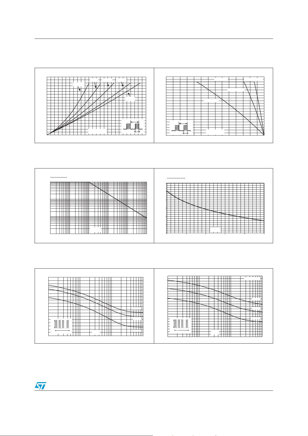
Figure 1. Average forward power dissipation
versus average forward current
(per diode)
P (W)
F(AV)
10
9
8
7
6
5
4
3
2
1
0
012345678 910111213
δ = 0.05
δ = 0.1
I (A)
F(AV)
δ = 0.2
δ = 0.5
δ
δ = 1
=tp/T
T
tp
Figure 3. Normalized avalanche power
derating versus pulse duration
P(t)
ARM p
P(1µs)
ARM
1
0.1
0.01
t(µs)
0.001
0.10.01 1
p
10 100 1000
Figure 2. Average forward current versus
ambient temperature
(δ = 0.5, per diode)
I (A)
F(AV)
11
10
9
8
7
6
5
4
3
2
1
0
0 25 50 75 100 125 150 175
δ
=tp/T
T
tp
R =15°C/W
th(j-a)
T (°C)
amb
R=R
th(j-a) th(j-c)
I²PAK/TO-220AB
TO-220FPAB
Figure 4. Normalized avalanche power
derating versus junction
temperature
P
(Tj)
ARM
P
(25°C)
ARM
1.2
1
0.8
0.6
0.4
0.2
0
25 50 75 100 125 150
T(°C)
j
Figure 5. Non repetitive surge peak forward
current versus overload duration
(maximum values, per diode)
I (A)
M
180
160
140
120
100
80
60
40
IM
20
0
1.E-03 1.E-02 1.E-01 1.E+00
δ=0.5
t
t(s)
T =25°C
a
T =75°C
a
T =125°C
a
Doc ID 11281 Rev 2 3/9
Figure 6. Non repetitive surge peak forward
current versus overload duration
(maximum values, per diode)
I (A)
M
120
110
100
90
80
70
60
50
40
30
I
M
20
10
0
1.E-03 1.E-02 1.E-01 1.E+00
t
δ
=0.5
t(s)
TO-220FPAB
T =25°C
a
T =75°C
a
T =125°C
a
 Loading...