

ST STPS20M100S User Manual
STPS20M100S
Power Schottky rectifier
Features
■ High current capability
■ Avalanche rated
■ Low forward voltage drop current
■ High frequency operation
■ Insulated package:
– Insulation voltage 2000 V rms
– Package capacitance = 12 pF
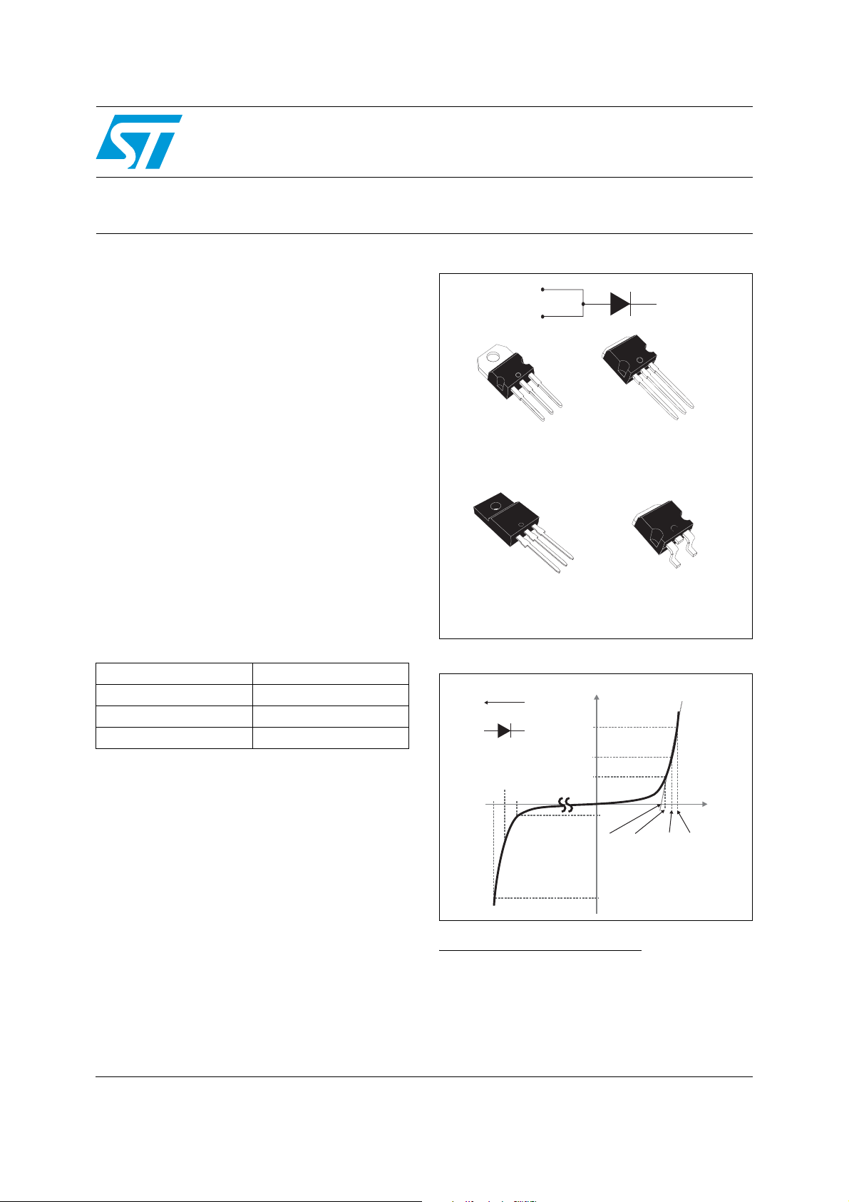
Description
This single Schottky rectifier is suited for high
frequency switch mode power supply.
20 A
100 V
2
PA K
Packaged in TO-220AB, TO-220FPAB, D
2
and I
PAK, this device is intended to be used in
notebook, game station and desktop adaptors,
providing in these applications a good efficiency
at both low and high load.
Table 1. Device summary
I
F(AV)
V
RRM
(max) 150 °C
T
j
(typ) 0.455 V
V
F
A(1)
K(2)
A(3)
K
A
A
K
TO-220AB
STPS20M100ST
A
2
PAK
I
STPS20M100SR
K
A
K
A
TO-220FPAB
STPS20M100SFP
STPS20M100SG-TR
A
2
PAK
D
Figure 1. Electrical characteristics
2 x I
I
"Forward"
F(Io)
X
X
V
F
O
I
F
I
O
I
R
V
V
To
V
I
V
RRM
V
V
AR
R
"Reverse"
A
K
(a)
V
F(2xIo)
A
V
I
AR
a. V
and I
ARM
operating area defined in Figure 14 V
pulse measurements (t
are static characteristics
must respect the reverse safe
ARM
< 1 µs). VR, IR, V
p
and IAR are
AR
RRM
and VF,
April 2010 Doc ID 15521 Rev 2 1/11
www.st.com
11

Characteristics STPS20M100S
1 Characteristics
Table 2. Absolute ratings (limiting values with terminals 1 and 3 short circuited)
Symbol Parameter Value Unit
V
I
F(RMS)
I
F(AV)
I
FSM
P
ARM
V
ARM
V
ASM
T
1. For temperature or pulse time duration deratings, refer to Figure 4. and Figure 5.. More details regarding the avalanche
energy measurements and diode validation in the avalanche are provided in the application notes AN1768 and AN2025.
2. Refer to Figure 14
3. condition to avoid thermal runaway for a diode on its own heatsink
Table 3. Thermal resistance
Repetitive peak reverse voltage 100 V
RRM
Forward current rms 30 A
2
Average forward current δ = 0.5
Surge non repetitive forward current
(1)
Repetitive peak avalanche power tp = 1 µs Tj = 25 °C 16000 W
Maximum repetitive peak avalanche
(2)
voltage
Maximum single pulse peak
(2)
avalanche voltage
Storage temperature range -65 to + 175 °C
stg
Maximum operating junction temperature
T
j
dPtot
--------------dTj
1
--------------------------
<
Rth j a–()
TO-220AB, D
TO-220FPAB, T
= 10 ms sinusoidal,
t
p
terminals 1 and 3 short circuited
tp < 1 µs Tj < 150 °C
IAR < 40 A
tp < 1 µs Tj < 150 °C
< 40 A
I
AR
(3)
PAK, I2PAK, Tc = 130 °C
= 85 °C
c
20 A
530 A
120 V
120 V
150 °C
Symbol Parameter Value Unit
2
R
th(j-c)
Table 4. Static electrical characteristics (terminals 1 and 3 short circuited)
Junction to case
TO-220AB, D
TO-220FPAB 4
PAK, I2PA K 1 .2
°C/W
Symbol Parameter Test conditions Min. Typ. Max. Unit
= 25 °C
(1)
I
R
V
F
1. Pulse test: tp = 5 ms, δ < 2%
2. Pulse test: t
Reverse leakage current
(2)
Forward voltage drop
= 380 µs, δ < 2%
p
T
j
= 125 °C 5 mA
T
j
= 25 °C
T
j
= 125 °C 10 40 mA
T
j
= 25 °C
T
j
T
= 125 °C 455
j
= 25 °C
T
j
T
= 125 °C 530 600
j
= 25 °C
T
j
= 125 °C 610 690
T
j
V
= 70 V
R
V
= 100 V
R
I
= 5 A
F
= 10A
I
F
I
= 20 A
F
5µA
10 40 µA
550
660 730
mV
775 850
To evaluate the conduction losses use the following equation:
P = 0.425 x I
2/11 Doc ID 15521 Rev 2
+ 0.0088 x I
F(AV)
F2(RMS)

STPS20M100S Characteristics
Figure 2. Average forward power dissipation
versus average forward current
PF(av)(W)
20
18
16
14
12
10
8
6
4
2
0
0 2 4 6 8 10 12 14 16 18 20 22 24 26 28
δ=0.05
δ=0.1
δ=0.2
I (av)(A)
F
δ=0.5
δ
=tp/T
δ=1
T
tp
Figure 4. Normalized avalanche power
derating versus pulse duration
P(t)
ARM p
P (1µs)
ARM
1
0.1
0.01
t (µs)
0.001
0.10.01 1
p
10 100 1000
Figure 3. Average forward current versus
ambient temperature (δ = 0.5)
I
(A)
(av)
F
22
20
18
16
14
12
10
8
6
4
2
0
T
tp
=tp/T
δ
0 25 50 75 100 125 150
R
th(j-a)=Rth(j-c)
TO-220FPAB
R
th(j-a)
T (°C)
amb
TO-220AB/I²PAK/D²PAK
=15°C/W
Figure 5. Normalized avalanche power
derating versus junction
temperature
P(T)
ARM j
P (25°C)
ARM
1.2
1
0.8
0.6
0.4
0.2
0
25 50 75 100 125 150
T (°C)
j
Figure 6. Non repetitive surge peak forward
current versus overload
duration, maximum values
I
(A)
M
280
Terminals 1 and 3 short circuited
240
200
160
120
80
I
M
40
0
1.E-03 1.E-02 1.E-01 1.E+00
t
=0.5
δ
t(s)
TO-220AB/I²PAK/D²PAK
TC=25°C
TC=75°C
TC=125°C
Doc ID 15521 Rev 2 3/11
Figure 7. Non repetitive surge peak forward
current versus overload duration,
maximum values
I
(A)
M
140
120
100
80
60
40
20
Terminals 1 and 3 short circuited
I
M
t
=0.5
0
1.E-03 1.E-02 1.E-01 1.E+00
δ
t(s)
TO-220FPAB
TC=25°C
TC=75°C
TC=125°C
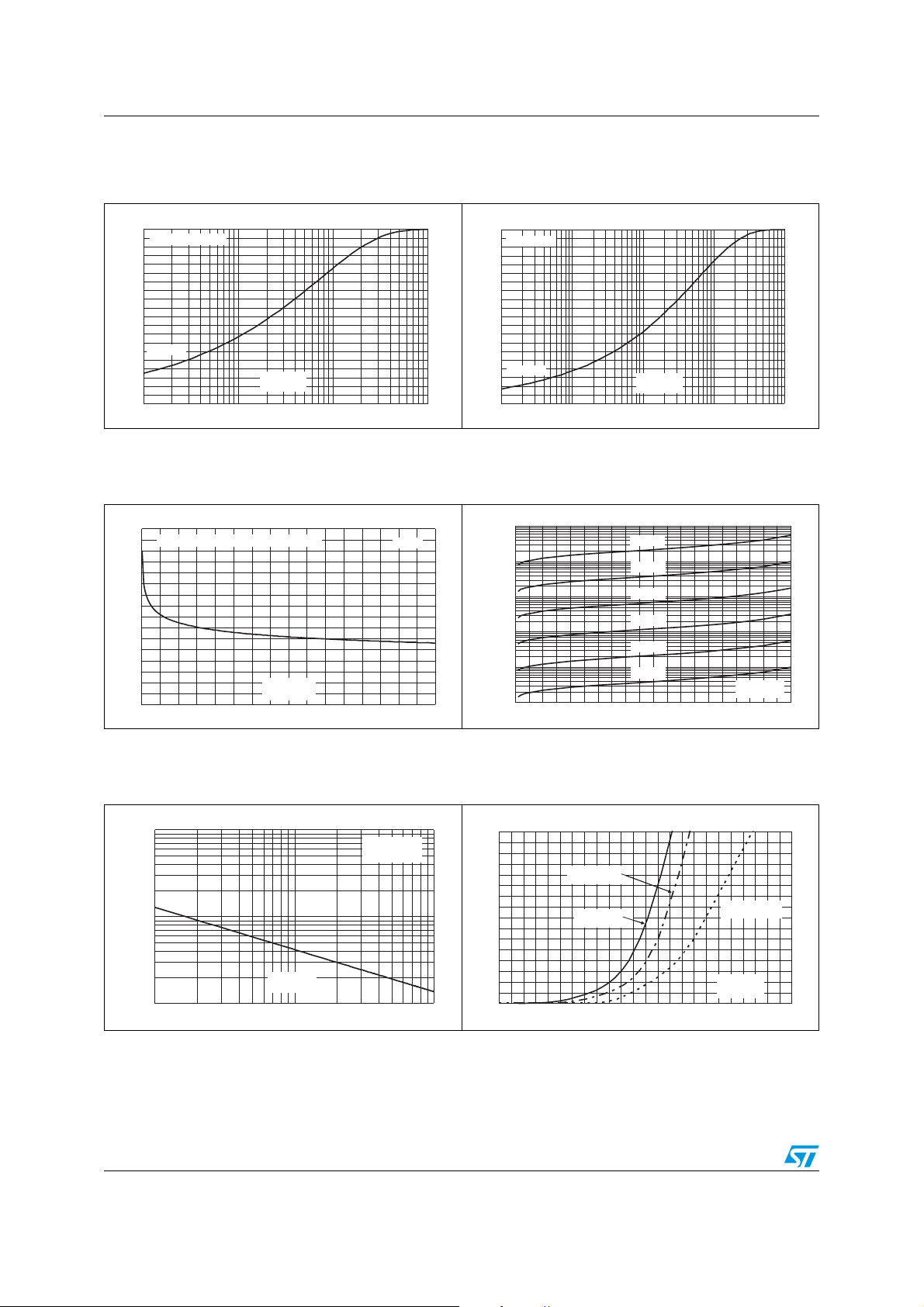
Characteristics STPS20M100S
Figure 8. Relative variation of thermal
impedance junction to case
versus pulse duration
Z
th(j-c)/Rth(j-c)
1.0
TO-220AB/I²PAK/D²PAK
0.9
0.8
0.7
0.6
0.5
0.4
Single pulse
0.3
0.2
0.1
0.0
1.E-03 1.E-02 1.E-01 1.E+00
tp(s)
Figure 10. Thermal resistance junction to
ambient versus copper surface
under tab
R
(°C/W)
th(j-a)
80
Epoxy printed board FR4, copper thickness = 35 µm)
70
60
50
40
30
20
10
0
0 5 10 15 20 25 30 35 40
SCu(cm²)
D²PAK
Figure 9. Relative variation of thermal
impedance junction to case versus
pulse duration
Z
th(j-c)/Rth(j-c)
1.0
TO-220FPAB
0.9
0.8
0.7
0.6
0.5
0.4
0.3
0.2
Single pulse
0.1
0.0
1.E-03 1.E-02 1.E-01 1.E+00 1.E+01
tp(s)
Figure 11. Reverse leakage current versus
reverse voltage applied (typical
values)
I
(mA)
R
1.E+02
1.E+01
1.E+00
1.E-01
1.E-02
1.E-03
0 102030405060708090100
Tj=150°C
Tj=125°C
Tj=100°C
Tj=75°C
Tj=50°C
Tj=25°C
VR(V)
Figure 12. Junction capacitance versus
Figure 13. Forward voltage drop versus
reverse voltage applied
(typical values)
C(pF)
10000
1000
VR(V)
100
1 10 100
V
F=1MHz
OSC
Tj=25°C
=30mV
RMS
4/11 Doc ID 15521 Rev 2
I
FM
40
35
30
25
20
15
10
5
0
0.0 0.1 0.2 0.3 0.4 0.5 0.6 0.7 0.8 0.9 1.0 1.1 1.2
forward current (terminals 1 and 3
short circuited)
(A)
Tj=125°C
Tj=125°C
(Maximum values)
(Maximum values)
Tj=125°C
Tj=125°C
(Typical values)
(Typical values)
Tj=25°C
(Maximum values)
V (V)
FM
 Loading...