

ST STPS20L25CT, STPS20L25CG User Manual
®
LOW DROP POWER SCHOTTKY RECTIFIER
MAIN PRODUCT CHARACTERISTICS
STPS20L25CT/CG
I
F(AV)
V
RRM
2x10A
25 V
Tj (max) 150 °C
V
(max) 0.35V
F
FEATURES AND BENEFITS
VERY LOW FORWARD VOLTAGE DROP FOR
n
LESS POWER DISSIPATION AND REDUCED
HEATSINK
OPTIMIZED CONDUCTION/REVERSE LOSSES
n
TRADE-OFF WHICH MEANS THE HIGHEST
EFFICIENCY IN THE APPLICATIONS
n
AVALANCHE CAPABILITY SPECIFIED
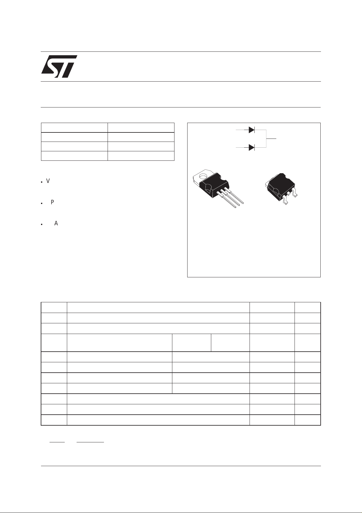
DESCRIPTION
Dual center tap Schottky rectifier suited to
Switched Mode Power Supplies and high
frequency DC to DC converters.
Packaged in TO-220AB and D
2
PAK, this device is
especially intended for use as a rectifier at the
secondary of 3.3V SMPS units.
ABSOLUTE RATINGS (limiting values, per diode)
A1
A2
A1
TO-220AB
STPS20L25CT
K
K
A2
K
A2
A1
D2PAK
STPS20L25CG
Symbol Parameter Value Unit
V
RRM
I
F(RMS)
I
F(AV)
I
FSM
I
RRM
I
RSM
P
ARM
T
stg
Repetitive peak reverse voltage 25 V
RMS forward current 30 A
Average forward current Tc = 145°C
δ = 0.5
Per diode
Per device
10
20
Surge non repetitive forward current tp = 10 ms Sinusoidal 220 A
Repetitive peak reverse current tp=2 µs square F=1kHz 1 A
Non repetitive peak reverse current tp = 100 µs square 3 A
Repetitive peak avalanche power tp = 1µs Tj = 25°C 5300 W
Storage temperature range - 65 to + 150 °C
Tj Maximum operating junction temperature * 150 °C
dV/dt Critical rate of rise of reverse voltage 10000 V/µs
dPtot
*:
<
dTj Rth j a
July 2003 - Ed : 4A
thermal runaway condition for a diode on its own heatsink
−1()
A
1/5

STPS20L25CT/CG
THERMAL RESISTANCES
Symbol Parameter Value Unit
R
th (j-c)
R
th (c)
When the diodes 1 and 2 are used simultaneously :
∆ Tj(diode 1) = P(diode1) x R
STATIC ELECTRICAL CHARACTERISTICS (per diode)
Symbol Tests conditions Tests conditions Min. Typ. Max. Unit
I
R
V
Pulse test: *tp=380µs,δ<2%
To evaluate the maximum conduction losses use the following equation :
P=0.22xI
Fig. 1: Average forward power dissipation versus
average forward current.
Junction to case Per diode 1.5 °C/W
Total 0.8
Coupling
(Per diode) + P(diode 2) x R
th(j-c)
* Reverse leakage current Tj = 25°CV
th(c)
R=VRRM
0.1
Tj = 125°C 125 250 mA
* Forwardvoltage drop Tj = 25°CI
F
Tj = 125°CI
Tj=25°CI
Tj = 125°CI
+ 0.013 I
F(AV)
F2(RMS)
= 10 A 0.46 V
F
= 10 A 0.30 0.35
F
= 20 A 0.56
F
= 20 A 0.41 0.48
F
Fig. 2: Average forward current versus ambient
temperature ( δ = 0.5).
800 µA
PF(av)(W)
5
4
3
2
1
0
01234567891011
δ = 0.05
δ = 0.1
IF(av) (A)
δ = 0.2
δ = 0.5
δ
=tp/T
δ = 1
T
tp
Fig. 3: Normalized avalanche power derating
versus pulse duration.
P(t)
ARM p
P (1µs)
ARM
1
0.1
0.01
t (µs)
0.001
0.10.01 1
p
10 100 1000
IF(av)(A)
12
10
8
6
4
2
0
0 25 50 75 100 125 150
δ
T
=tp/T
Rth(j-a)=50°C/W
tp
Rth(j-a)=Rth(j-c)
Tamb(°C)
Fig. 4: Normalized avalanche power derating
versus junction temperature.
P(t)
ARM p
P (25°C)
ARM
1.2
1
0.8
0.6
0.4
0.2
0
0 25 50 75 100 125 150
T (°C)
j
2/5
 Loading...