

ST STPS20120C User Manual
Features
■ High junction temperature capability
■ Avalanche rated
■ Low leakage current
■ Good trade-off between leakage current and
forward voltage drop
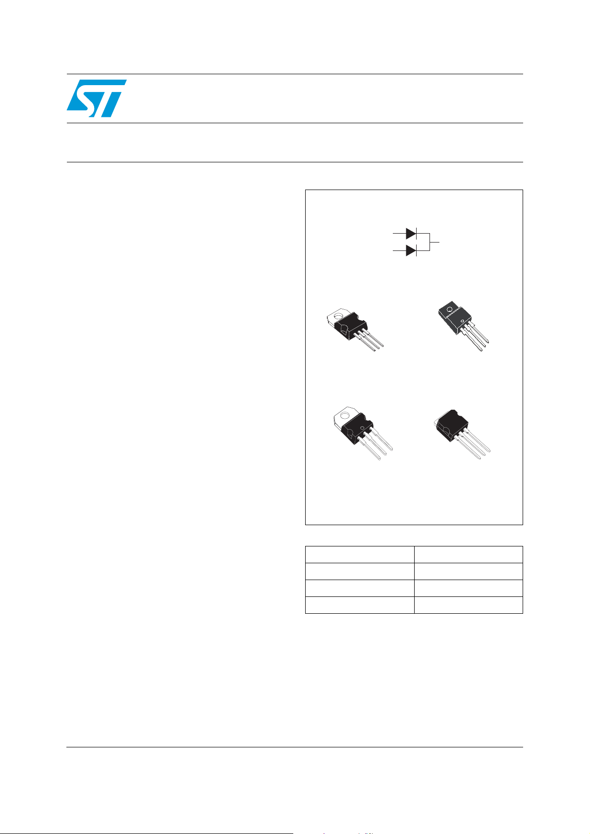
STPS20120C
Power Schottky rectifier
Datasheet − production data
A1
K
A2
Description
Dual center tap Schottky rectifier suited for high
frequency switch mode power supply.
Packaged in TO-220AB, TO-220AB narrow leads,
2
I
PAK and TO-220FPAB, this device is intended to
be used in notebook and LCD adaptors, desktop
SMPS, providing in these applications a margin
between the remaining voltages applied on the
diode and the voltage capability of the diode.
K
A2
K
A1
TO-220AB
STPS20120CT
K
A2
A1
K
TO-220AB narrow leads
STPS20120CTN
Table 1. Device summary
I
2 x 10 A
F(AV)
V
120 V
RRM
T
j(max)
0.54 V
V
F(typ)
A2
K
A1
TO-220FPAB
STPS20120CFP
A2
K
A1
2
I
PAK
STPS20120CR
175 °C
June 2012 Doc ID 11212 Rev 3 1/10
This is information on a product in full production.
www.st.com
10

Characteristics STPS20120C
1 Characteristics
Table 2. Absolute ratings (limiting values, per diode)
Symbol Parameter Value Unit
V
RRM
I
F(RMS)
I
F(AV)
I
FSM
P
ARM
T
dPtot
---------------
1. condition to avoid thermal runaway for a diode on its own heatsink
dTj
Repetitive peak reverse voltage 120 V
RMS forward current 30 A
Average forward current, δ = 0.5
TO-220AB, I2PAK,
TO-220AB narrow
leads
TO-220FPAB
Tc = 150 °C
Tc = 145 °C 20
T
= 125 °C
c
T
= 100 °C 20
c
Per diode
Per device
Per diode
Per device
Surge non repetitive forward current tp = 10 ms Sinusoidal 150 A
Repetitive peak avalanche power tp = 1 µs Tj = 25 °C 4600 W
Storage temperature range -65 to + 175 °C
stg
Maximum operating junction temperature
T
j
1
--------------------------
<
Rth j a–()
(1)
10
10
175 °C
Table 3. Thermal parameters
Symbol Parameter Value Unit
R
R
th(j-c)
th(c)
Junction to case
Coupling
I2PAK, TO-220AB,
TO-220AB narrow leads
TO-220FPAB
Per diode
To ta l
Per diode
To ta l
I2PAK, TO-220AB
TO-220AB narrow leads
To ta l
TO-220FPAB 3.5
3
1.8
5.5
4.5
0.6
°C/W
A
When the diodes 1 and 2 are used simultaneously:
T
(diode 1) = P(diode 1) x R
j
2/10 Doc ID 11212 Rev 3
(per diode) + P(diode 2) x R
th(j-c)
th(c)
STPS20120C Characteristics
Table 4. Static electrical characteristics (per diode)
Symbol Test conditions Min. Typ. Max. Unit
(1)
I
R
V
Reverse leakage current
(2)
Forward voltage drop
F
1. Pulse test: tp = 5 ms, δ < 2%
2. Pulse test: tp = 380 µs,
δ < 2%
Tj = 25 °C
VR = V
= 125 °C 1.5 5 mA
T
j
T
= 25 °C
j
= 125 °C 0.54 0.58
T
j
= 25 °C
T
j
Tj = 125 °C 0.7 0.74
T
= 25 °C
j
= 125 °C 0.81 0.86
T
j
RRM
= 2.5 A
I
F
= 10 A
I
F
IF = 20 A
10 µA
0.7
0.92
1.02
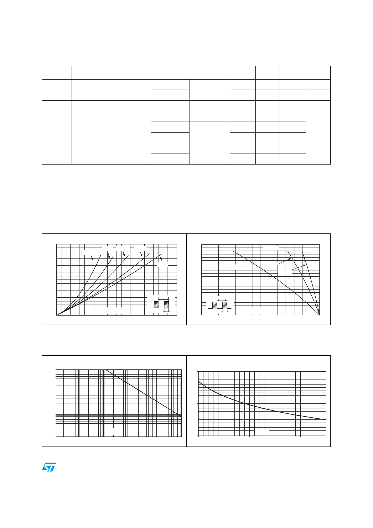
To evaluate the maximum conduction losses use the following equation:
P = 0.62 x I
Figure 1. Average forward power dissipation
versus average forward current
(per diode)
P (W)
F(AV)
10
9
8
7
6
5
4
3
2
1
0
012345678910111213
δ = 0.05
δ = 0.1
Figure 3. Normalized avalanche power
derating versus pulse duration
F(AV)
δ = 0.2
I (A)
F(AV)
+ 0.012 I
δ = 0.5
F2(RMS)
δ = 1
T
=tp/T
δ
Figure 2. Average forward current versus
ambient temperature
(
δ = 0.5, per diode)
I (A)
F(AV)
11
10
9
8
7
6
5
4
3
2
tp
1
=tp/T
δ
0
0 25 50 75 100 125 150 175
T
R =15°C/W
th(j-a)
tp
R=R
TO-220FPAB
T (°C)
amb
th(j-a) th(j-c)
TO-220AB
Figure 4. Normalized avalanche power
derating versus junction
I²PAK
temperature
P(t)
ARM p
P (1µs)
ARM
1
P (25°C)
1.2
P(t)
ARM p
ARM
V
0.01
0.001
1
0.1
t (µs)
p
0.10.01 1
10 100 1000
0.8
0.6
0.4
0.2
0
25 50 75 100 125 150
T (°C)
j
Doc ID 11212 Rev 3 3/10
 Loading...