

ST STPS200170TV1 User Manual
Features
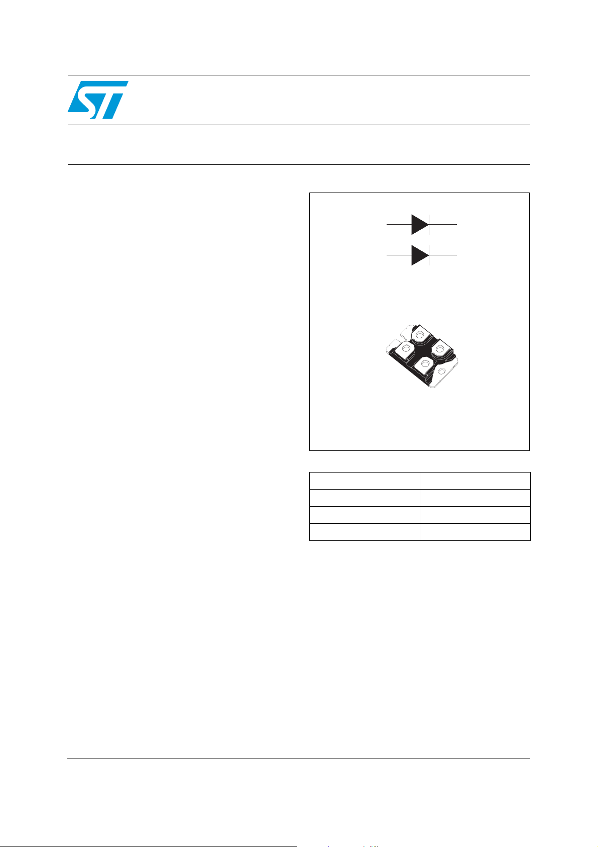
STPS200170TV1
High voltage power Schottky rectifier
■ Negligible switching losses
■ Avalanche rated
■ Low leakage current
■ Good trade-off between leakage current and
forward voltage drop
■ Insulated package: ISOTOP
– Electrical insulation = 2500 V rms,
capacitance = 45 pF
Description
This high voltage Schottky rectifier is suited for
high frequency switch mode power supplies.
Packaged in ISOTOP, this device is intended for
use in the secondary rectification of applications.
A1 K1
A2 K2
A2
A1
K1
ISOTOP
Table 1. Device summary
I
F(AV)
V
RRM
T
j
(typ) 0.63 V
V
F
K2
2 x 100 A
170 V
150 °C
September 2011 Doc ID 11857 Rev 2 1/7
www.st.com
7
Characteristics STPS200170TV1
1 Characteristics
Table 2. Absolute ratings - limiting values per diode at T
= 25 °C, unless otherwise specified
amb
Symbol Parameter Value Unit
V
RRM
I
F(RMS)
I
F(AV)
I
FSM
P
ARM
T
1. condition to avoid thermal runaway for a diode on its own heatsink
Repetitive peak reverse voltage 170 V
Forward rms current 200 A
Average forward current, δ = 0.5 Tc = 105 °C per diode 100 A
Surge non repetitive forward current tp = 10 ms sinusoidal 700 A
= 1 µs, Tj = 25 °C
Repetitive peak avalanche power
Storage temperature range -55 to + 150 °C
stg
Maximum operating junction temperature
T
j
dP
tot
j
1
--------------------------<
R
th j a–()
--------------dT
t
p
(1)
100000 W
150 °C
Table 3. Thermal parameters
Symbol Parameter Value Unit
Per diode 0.52
R
R
th(j-c)
th(c)
Junction to case
°C/WTo t al 0 . 31
Coupling thermal resistance 0.1
When the diodes are used simultaneously:
T
j(diode1)
= P
(diode1)
X R
(per diode) + P
th(j-c)
(diode2)
X R
th(c)
Table 4. Static electrical characteristics
Symbol Parameter Test conditions Min. Typ. Max. Unit
(1)
I
R
V
1. Pulse test: tp = 5 ms, δ < 2 %
2. Pulse test: t
Reverse leakage current
(2)
Forward voltage drop
F
= 380 µs, δ < 2 %
p
= 25 °C
T
j
= 125 °C - 30 100 mA
T
j
Tj = 25 °C
= 150 °C - 0.63 0.68
T
j
= 25 °C IF = 200 A - - 0.975
T
j
= 150 °C - 0.78 0.86
T
j
V
= V
R
I
= 100 A
F
RRM
--200µA
- - 0.85
To evaluate the conduction losses use the following equation:
P = 0.5 x I
+ 0.0018 I
F(AV)
F2(RMS)
V
2/7 Doc ID 11857 Rev 2
STPS200170TV1 Characteristics
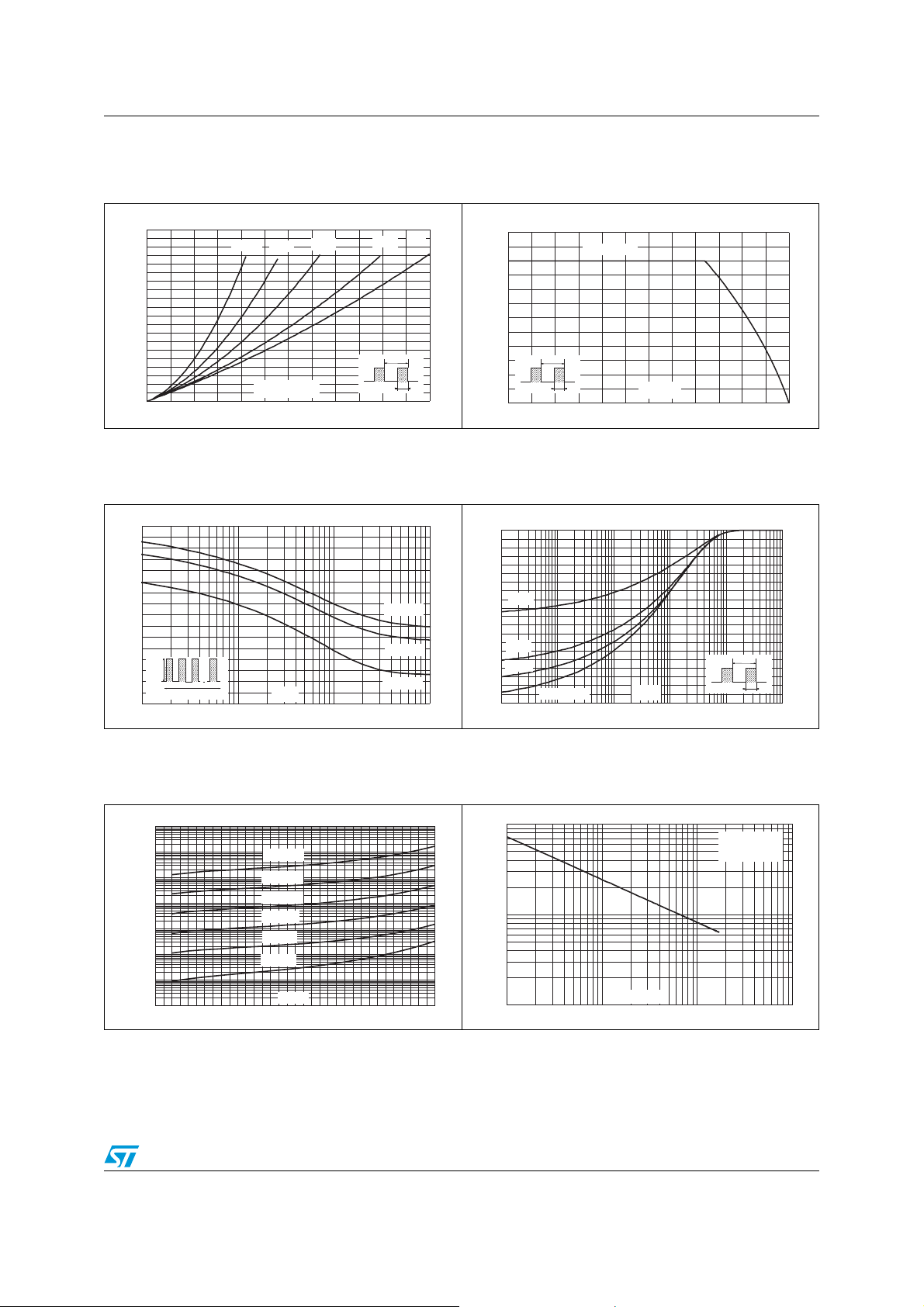
Figure 1. Conduction losses versus average
current (per diode)
P
(W)
F(AV)
100
90
80
70
60
50
40
30
20
10
0
0 20 40 60 80 100 120
δ=0.05
δ=0.1
I
F(AV)
δ=0.2
(A)
δ
δ=0.5
=t /T
p
δ=1
T
t
p
Figure 3. Non-repetitive surge peak forward
current vesus overload duration
(maximum values per diode)
IM(A)
800
700
600
500
400
300
200
I
M
100
0
1.E-03 1.E-02 1.E-01 1.E+00
t
d
=0.5
t(s)
TC=50°C
TC=75°C
TC=125°C
Figure 2. Average forward current versus
ambient temperature
(δ = 0.5, per diode)
I
(A)
F(AV)
120
R
100
80
60
40
20
0
T
=tp/T
δ
0 25 50 75 100 125 150
th(j-a)=Rth(j-c)
tp
T
(°C)
amb
Figure 4. Relative variation of thermal
impedance (junction to case) versus
pulse duration
Z
(j ) (j )
th -c/Rth -c
1.0
0.9
0.8
0.7
δ=0.5
0.6
0.5
0.4
δ=0.2
0.3
δ=0.1
0.2
0.1
0.0
1.E-04 1.E-03 1.E-02 1.E-01 1.E+00 1.E+01
Single pulse
tP(s)
δ
=tp/T
T
tp
Figure 5. Reverse leakage current versus
reverse voltage applied (typical
values per diode)
IR(mA)
1.E+03
1.E+02
1.E+01
1.E+00
1.E-01
1.E-02
1.E-03
1.E-04
0 10 20 30 40 50 60 70 80 90 100 110 120 130 140 150 160 170
Tj=150°C
Tj=125°C
Tj=100°C
Tj=75°C
Tj=50°C
Tj=25°C
VR(V)
Doc ID 11857 Rev 2 3/7
Figure 6. Junction capacitances versus
reverse voltage applied (typical
values per diode)
C(pF)
10000
1000
100
1 10 100 1000
VR(V)
V
F=1MHz
OSC
Tj=25°C
=30mV
RMS
 Loading...