

ST STPS1L40 User Manual

Features
■ Very small conduction losses
■ Negligible switching losses
■ Low forward voltage drop
■ Surface mount miniature packages
■ Avalanche capability specified
Description
STPS1L40
Low drop power Schottky rectifier
A
K
SMA
(JEDEC DO-214AC)
STPS1L40A
K
SMB
(JEDEC DO-214AA)
STPS1L40U
A
Single chip Schottky rectifiers suited to switched
mode power supplies and high frequency DC to
DC converters.
Packaged in SMA, SMB and STmite flat this
device is especially intended for surface mounting
and used in low voltage, high frequency inverters,
free wheeling and polarity protection applications.
A
K
STmite flat
STPS1L40MF
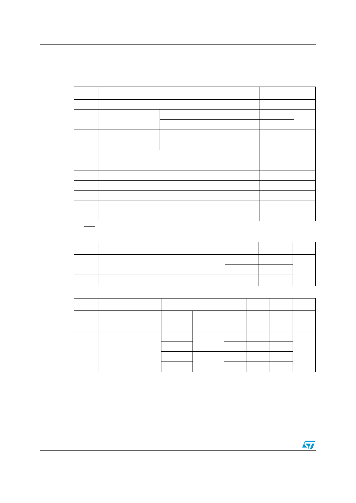
Table 1. Device summary
Symbol Value
I
F(AV)
V
RRM
(max) 150 °C
T
j
(max) 0.42 V
V
F
1 A
40 V
June 2009 Doc ID 5507 Rev 6 1/11
www.st.com
11
Characteristics STPS1L40
1 Characteristics
Table 2. Absolute ratings (limiting values)
Symbol Parameter Value Unit
V
Repetitive peak reverse voltage 40 V
RRM
SMA / SMB 8
I
F(RMS)
I
F(AV)
I
I
I
P
T
Forward rms current
STmite flat 2
Average forward current
SMA / SMB T
STmite flat T
Surge non repetitive forward current tp = 10 ms sinusoidal 60 A
FSM
Repetitive peak reverse current tp = 2 µs F = 1 kHz square 1 A
RRM
Non repetitive peak reverse current tp = 100 µs square 1 A
RSM
Repetitive peak avalanche power tp = 1 µs Tj = 25 °C 900 W
ARM
Storage temperature range - 65 to + 150 °C
stg
Maximum operating junction temperature
T
j
= 130 °C δ = 0.5
L
= 135 °C δ = 0.5
C
(1)
1A
150 °C
dV/dt Critical rate of rise of reverse voltage 10000 V/µs
<
Rth(j-a)
1
dPtot
1. condition to avoid thermal runaway for a diode on its own heatsink
dTj
Table 3. Thermal resistance
Symbol Parameter Value Unit
SMA 30
R
R
Table 4. Static electrical characteristics
th(j-l)
th(j-c)
Junction to lead
Junction to case
SMB 25
STmite flat 20
°C/W
A
Symbol Parameter Tests conditions Min. Typ. Max. Unit
T
= 25 °C
(1)
I
Reverse leakage current
R
(1)
V
1. Pulse test: tp = 380 µs, δ < 2%
Forward voltage drop
F
j
= 125 °C - 6 10 mA
T
j
= 25 °C
T
j
T
= 125 °C - 0.37 0.42
j
= 25 °C
T
j
T
= 125 °C - 0.5 0.61
j
V
I
F
I
F
To evaluate the conduction losses use the following equation:
P = 0.23 x I
2/11 Doc ID 5507 Rev 6
F(AV)
+ 0.19 I
F2(RMS)
= V
R
= 1 A
= 2 A
- - 35 µA
RRM
--0.5
V
- - 0.63
STPS1L40 Characteristics
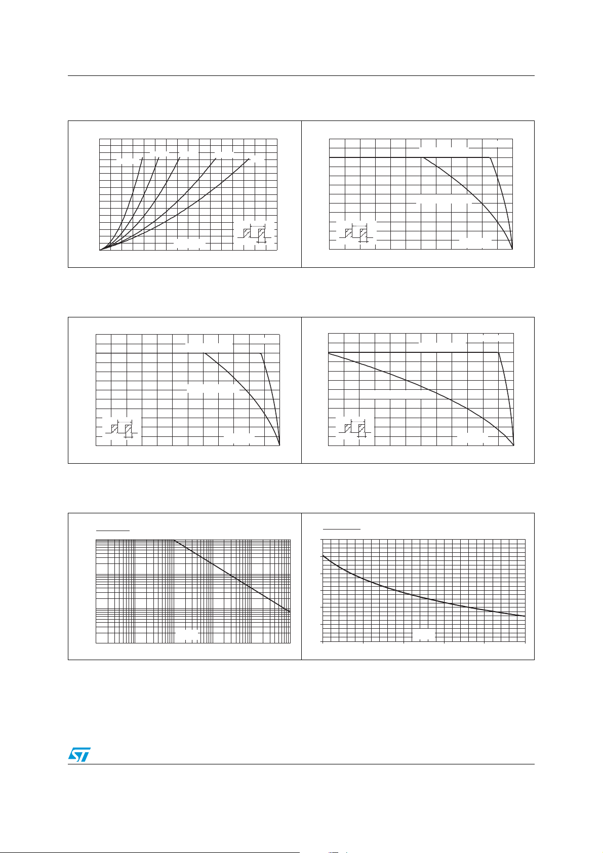
Figure 1. Average forward power dissipation
versus average forward current
P
(W)
F(AV)
0.8
0.7
δ = 0.05
0.6
0.5
0.4
0.3
0.2
0.1
0.0
0.0 0.2 0.4 0.6 0.8 1.0 1.2 1.4 1.6
δ = 0.1
δ = 0.2
I
F(AV)
(A)
δ = 0.5
δ = 1
δ = tp/T
T
t
p
Figure 3. Average forward current versus
ambient temperature (SMB, δ = 0.5)
I
(A)
F(AV)
1.2
R
= R
th(j-a)
R
th(j-a)
th(j-l)
= 100 °C/W
T
1.0
0.8
0.6
0.4
0.2
0.0
T
δ = tp/T
0 25 50 75 100 125 150
t
p
amb
SMB
(°C)
Figure 2. Average forward current versus
ambient temperature (SMA, δ = 0.5)
I
(A)
F(AV)
1.2
R
= R
th(j-a)
1.0
0.8
0.6
0.4
0.2
0.0
T
δ = tp/T
0 25 50 75 100 125
t
p
R
th(j-a)
th(j-l)
= 120 °C/W
T
amb
SMA
(°C)
Figure 4. Average forward current versus
ambient temperature
(STmite flat, δ = 0.5)
I
(A)
F(AV)
1.2
R
= R
th(j-a)
1.0
0.8
0.6
0.4
0.2
δ = tp/T
0.0
0 25 50 75 100 125
R
= 250 °C/W
th(j-a)
T
t
p
th(j-c)
T
amb
STmite flat
(°C)
150
150
Figure 5. Normalized avalanche power
derating versus pulse duration
P(tp)
ARM
P (1 µs)
ARM
1
0.1
0.01
t (µs)
0.001
0.10.01 1
p
10 100 1000
Figure 6. Normalized avalanche power
derating versus junction
temperature
P(Tj)
ARM
P (25 °C)
ARM
1.2
1
0.8
0.6
0.4
0.2
0
25 50 75 100 125 150
Doc ID 5507 Rev 6 3/11
T (°C)
j

Characteristics STPS1L40
Figure 7. Non repetitive surge peak forward
current versus overload duration
(maximum values, SMA)
IM(A)
7
6
5
4
3
2
I
M
1
0
1.E-04 1.E-03 1.E-02 1.E-01 1.E+00
δ = 0.5
t
t(s)
SMA
Ta= 25 °C
Ta= 75 °C
Ta= 125 °C
Figure 9. Non repetitive surge peak forward
current versus overload duration
(maximum values, STmite flat)
IM(A)
16
14
12
10
8
6
4
I
M
2
0
1.E-04 1.E-03 1.E-02 1.E-01 1.E+00
δ = 0.5
t
t(s)
STmite flat
Tc= 25 °C
Tc= 75 °C
Tc= 125 °C
Figure 8. Non repetitive surge peak forward
current versus overload duration
(maximum values, SMB)
IM(A)
7
6
5
4
3
2
I
M
1
0
1.E-04 1.E-03 1.E-02 1.E-01 1.E+00
δ
= 0.5
t
SMB
Ta= 25 °C
Ta= 75 °C
Ta= 125 °C
Figure 10. Relative variation of thermal
impedance junction to ambient
versus pulse duration (SMA)
Z
th(j-a)/Rth(j-a)
1.0
SMA
0.9
Epoxy printed circuit board,
0.8
copper thickness = 35 µm,
recommended pad layout
0.7
0.6
0.5
0.4
0.3
0.2
Single pulse
0.1
0.0
1.E-02 1.E-01 1.E+00 1.E+01 1.E+02 1.E+03
tp(s)
Figure 11. Relative variation of thermal
Figure 12. Relative variation of thermal
impedance junction to ambient
versus pulse duration (SMB)
Z
th(j-a)/Rth(j-a)
1.0
SMB
0.9
Epoxy printed circuit board,
0.8
copper thickness = 35 µm,
recommended pad layout
0.7
0.6
0.5
0.4
0.3
0.2
Single pulse
0.1
0.0
1.E-02 1.E-01 1.E+00 1.E+01 1.E+02 1.E+03
tp(s)
4/11 Doc ID 5507 Rev 6
Z
th(j-a)/Rth(j-a)
1.0
STmite flat
0.9
0.8
0.7
0.6
0.5
0.4
0.3
0.2
0.1
0.0
1.E-02 1.E-01 1.E+00 1.E+01 1.E+02 1.E+03
impedance junction to ambient
versus pulse duration (STmite flat)
Epoxy printed circuit board,
copper thickness = 35 µm,
recommended pad layout
Single pulse
tp(s)
 Loading...