

Features
■ Negligible switching losses
■ High junction temperature capability
■ Low leakage current
■ Good trade-off between leakage current and
forward voltage drop
■ Avalanche capability specified
Description
Schottky rectifier designed for high frequency
miniature switch mode power supplies such as
adaptors and on-board DC/DC convertors. This
device is packaged in STmite flat.
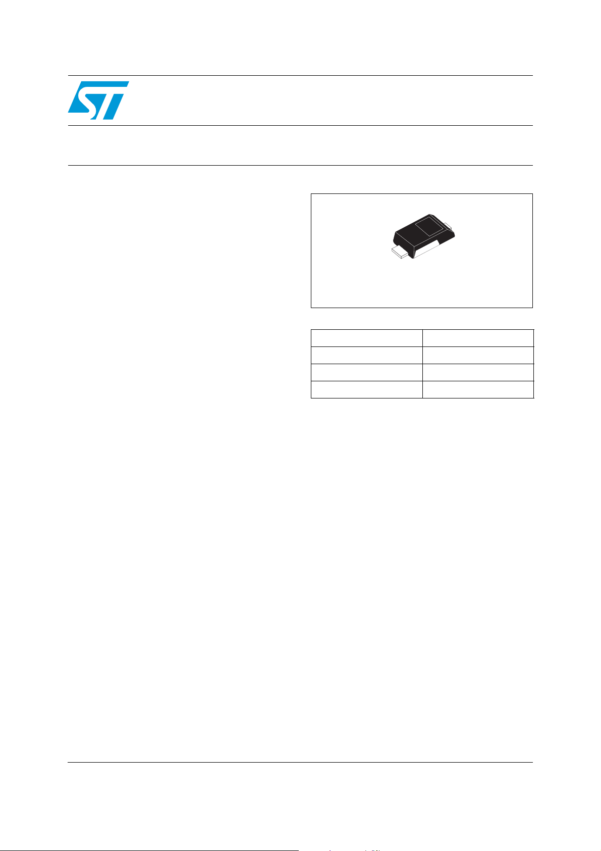
STPS1H100MF
High voltage power Schottky rectifier
A
K
STmite flat
(DO222-AA)
Table 1. Device summary
I
F(AV)
V
RRM
(max) 175 °C
T
j
V
(max) 0.62 V
F
1 A
100 V
May 2008 Rev 1 1/7
www.st.com

Characteristics STPS1H100MF
1 Characteristics
Table 2. Absolute ratings (limiting values)
Symbol Parameter Value Unit
V
RRM
I
F(RMS)
I
F(AV)
I
FSM
I
RRM
I
RSM
P
ARM
T
T
Repetitive peak reverse voltage 100 V
Forward current rms 2 A
Average forward current Tc = 160 °C δ = 0.5 1 A
Surge non repetitive forward current tp = 10 ms sinusoidal 50 A
Repetitive peak reverse current tp = 2 µs, F = I kHz square 1 A
Non-repetitive peak reverse current tp = 100 µs square 1 A
Repetitive peak avalanche power tp = 1 µs Tj = 25 °C 1500 W
Storage temperature range -65 to + 175 °C
stg
Maximum operating junction temperature
j
(1)
175 °C
dV/dt Critical rate of rise of reverse voltage (rated VR, Tj = 25 °C) 10000 V/µs
dPtot
---------------
1. condition to avoid thermal runaway for a diode on its own heatsink
dTj
Table 3. Thermal resistance
1
--------------------------
<
Rth j a–()
Symbol Parameter Value Unit
R
th(j-c)
Table 4. Static electrical characteristics
Junction to case 20 °C/W
Symbol Parameter Tests conditions Min. Typ Max. Unit
(1)
I
R
V
1. Pulse test: = 5 ms, δ < 2%
2. Pulse test: = 380 µs, δ < 2%
Reverse leakage current
(2)
Forward voltage drop
F
Tj = 25 °C
VR = V
= 1 A
I
F
I
= 2 A
F
RRM
= 125 °C 0.2 0.5
T
j
= 25 °C
T
j
T
= 125 °C 0.58 0.62
j
= 25 °C
T
j
= 125 °C 0.65 0.7
T
j
4µA
0.77
0.86
mA
V
To evaluate the conduction losses use the following equation: P = 0.54 x I
2/7
F(AV)
+ 0.08 I
F2(RMS)
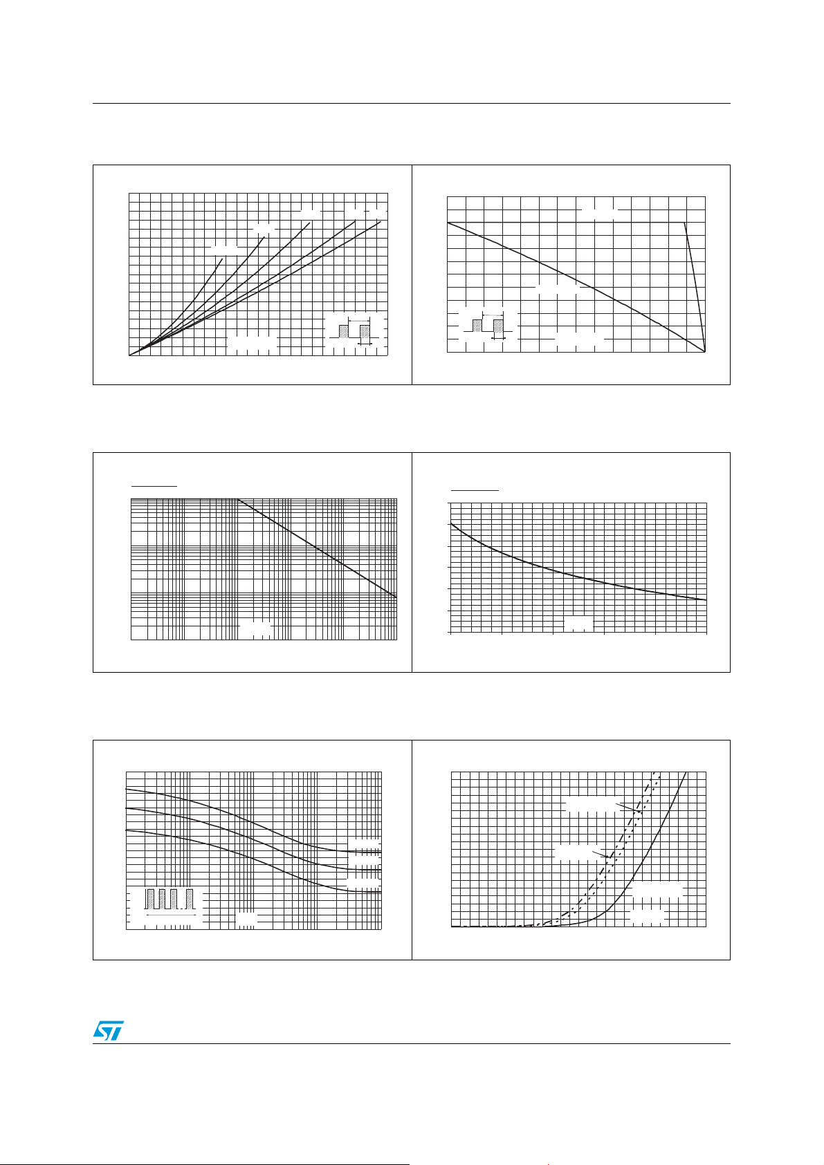
STPS1H100MF Characteristics
Figure 1. Average forward power dissipation
versus average forward current
P (W)
F(AV)
0.9
0.8
0.7
0.6
0.5
0.4
0.3
0.2
0.1
0.0
0.0 0.1 0.2 0.3 0.4 0.5 0.6 0.7 0.8 0.9 1.0 1.1 1.2
δ=0.05
δ=0.1
I (A)
F(AV)
δ=0.2
δ
=tp/T
δ=0.5
δ=1
T
tp
Figure 3. Normalized avalanche power
derating versus pulse duration
P(t)
ARM p
P (1µs)
ARM
1
0.1
0.01
t (µs)
0.001
0.10.01 1
p
10 100 1000
Figure 2. Average forward current versus
ambient temperature (δ = 0.5)
I (A)
F(AV)
1.2
R
=250°C/W
T (°C)
amb
th(j-a)=Rth(j-c)
1.0
0.8
0.6
R
0.4
0.2
0.0
0 25 50 75 100 125 150 175
δ
T
=tp/T
th(j-a)
tp
Figure 4. Normalized avalanche power
derating versus junction
temperature
P(Tj)
ARM
P (25°C)
ARM
1.2
1
0.8
0.6
0.4
0.2
0
25 50 75 100 125 150
T (°C)
j
Figure 5. Non repetitive surge peak forward
current versus overload duration
(maximum values)
I (A)
M
22
20
18
16
14
12
10
8
6
I
M
4
2
0
1.E-04 1.E-03 1.E-02 1.E-01 1.E+00
t
=0.5
δ
t(s)
Tc=25 °C
Tc=75 °C
Tc=125 °C
Figure 6. Forward voltage drop versus
forward current
I (A)
FM
20.0
18.0
16.0
14.0
12.0
10.0
8.0
6.0
4.0
2.0
0.0
0.0 0.1 0.2 0.3 0.4 0.5 0.6 0.7 0.8 0.9 1.0 1.1 1.2 1.3 1.4
3/7
Tj=125 °C
Tj=125 °C
(Maximum values)
(Maximum values)
Tj=125 °C
Tj=125 °C
(Typical values)
(Typical values)
Tj=25 °C
(Maximum values)
V (V)
FM
 Loading...