

ST STP7NK30Z, STF7NK30Z User Manual
现货库存、技术资料、百科信息、热点资讯,精彩尽在鼎好!
N-CHANNEL 300V - 0.80Ω - 5A TO-220/TO-220FP
Zener-Protected SuperMESH™MOSFET
STP7NK30Z
STF7NK30Z
Table 1: General Features
TYPE V
STP7NK30Z
STF7NK30Z
■ TYPICAL R
■ EXTREMELY HIGH dv /d t CAPABILITY
■ 100% AVALANCHE TESTED
■ GATE CHARGE MINIMIZED
■ VERY LOW INTRINSIC CAPACITANCES
■ VERY GOOD MANUFACTURING
DSSRDS(on)
300 V
300 V
(on) = 0.80 Ω
DS
< 0.9 Ω
< 0.9 Ω
I
D
5 A
5 A
Pw
50 W
20 W
REPEATIBILITY
DESCRIPTION
The SuperMESH™ series is obtained through an
extreme optimization of ST’s well established
strip-based PowerMESH™ layout. In addition to
pushing on-resistance significantly down, special
care is taken to ensure a very good dv/dt capability
for the most demanding applications. Such series
complements ST full range of high voltage MOSFETs including revolutionary MDmesh™ product
APPLICATIONS
■ HIGH CURRENT, HIGH SPEED SWITCHING
■ IDEAL F OR OFF-LINE POWER SUP PLIE S,
ADAPTORS AND PFC
■ LIGHTING
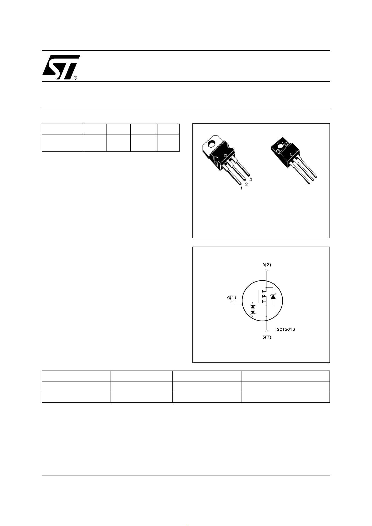
Figure 1: Package
TO-220
TO-220FP
Figure 2: Internal Schematic Diagram
3
2
1
Table 2: Order Codes
SALES TYPE MARKING PACKAGE PACKAGING
STF7NK30Z F7NK30Z TO-220FP TUBE
STP7NK30Z P7NK30Z TO-220 TUBE
Rev. 2
1/12September 2005
STP7NK30Z - STF7NK30Z
Table 3: Absolute Maximum ratings
Symbol Parameter Value Unit
STP7NK30Z STF7NK30Z
V
DS
V
DGR
V
GS
I
D
I
D
I
()
DM
P
TOT
V
ESD(G-S)
dv/dt (1) Peak Diode Recovery voltage slope 4.5 V/ns
V
ISO
T
j
T
stg
() Pulse width limited by safe operat i ng area
(1) I
≤5.7A, di/dt ≤200A/µs, VDD ≤ V
SD
(*) Limited only by maximum temperature allowed
Drain-source Voltage (VGS = 0)
Drain-gate Voltage (RGS = 20 kΩ)
300 V
300 V
Gate- source Voltage ± 30 V
Drain Current (continuous) at TC = 25°C
Drain Current (continuous) at TC = 100°C
55 (*)A
3.2 3.2 (*) A
Drain Current (pulsed) 20 20 (*) A
Total Dissipation at TC = 25°C
50 20 W
Derating Factor 0.4 0.16 W/°C
Gate source ESD(HBM-C=100pF, R=1.5KΩ) 2800 V
Insulation Withstand Voltage (DC) - 2500 V
Operating Junction Temperature
Storage Temperature
, Tj ≤ T
(BR)DSS
JMAX.
-55 to 150
-55 to 150
°C
°C
Table 4: Thermal Data
TO-220 TO-220FP
Rthj-case Thermal Resistance Junction-case Max 2.50 6.25 °C/W
Rthj-amb Thermal Resistance Junction-ambient Max 62.5 °C/W
T
l
Maximum Lead Temperature For Soldering Purpose
300 °C
Table 5: Avalanche Characteristics
Symbol Parameter Max Value Unit
I
AR
E
AS
Avalanche Current, Repetitive or Not-Repetitive
(pulse width limited by T
max)
j
Single Pulse Avalanche Energy
(starting T
= 25 °C, ID = IAR, VDD = 50 V)
j
5A
130 mJ
Table 6: Gate-Source Zener Diode
Symbol Parame ter Test Conditions Min. Typ. Max. Unit
BV
GSO
Gate-Source Breakdown
Igs=± 1mA (Open Drain) 30 V
Voltage
PROTECTION FEATURES OF GATE-TO-SOURCE ZENER DIODES
The built-in back-to-back Zener diodes have specifically been designed t o enhance not only t he device’s
ESD capability, but also to make them safely absorb possible voltage transients that may occasionally be
applied from gate to source. In this respect the Zener voltage is appropriate to achieve an efficient and
cost-effective intervention to p r otect the device’s integrity. These integrated Zener diodes thus avoid the
usage of external components.
2/12
STP7NK30Z - STF7NK30Z
ELECTRICAL CHARACTERISTICS (T
=25°C UNLESS OTHERWISE SPECIFIED)
CASE
Table 7: On /Off
Symbol Parameter Test Conditions Min. Typ. Max. Unit
V
(BR)DSS
Drain-source
ID =1 mA, VGS = 0 300 V
Breakdown Voltage
I
DSS
I
GSS
V
GS(th)
R
DS(on)
Zero Gate Voltage
Drain Current (V
GS
= 0)
Gate-body Leaka ge
Current (V
DS
= 0)
Gate Threshold Voltage
Static Drain-source On
V
= Max Rating
DS
V
= Max Rating, TC = 125 °C
DS
V
= ± 20V ±10 µA
GS
V
= VGS, ID = 50µA
DS
3 3.75 4.5 V
1
50
VGS = 10V, ID = 2.5 A 0.80 0.90 Ω
Resistance
Table 8: Dynamic
Symbol Parameter Test Conditions Min. Typ. Max. Unit
g
(1) Forward Transconductance VDS =15 V, ID=2.5 A 2.5 S
fs
C
oss eq.
C
C
C
t
d(on)
t
d(off)
t
r(Voff)
t
Q
Q
Q
iss
oss
rss
t
r
t
f
t
f
c
gs
gd
Input Capacitance
Output Capacitance
Reverse Transfer Capacitance
(3)
Equivalent Outpu t Capacitance
Turn-on Delay Time
Rise Time
Turn-off-Delay Time
Fall Time
Off-voltage Rise Time
Fall Time
Cross-over Time
g
Total Gate Charge
Gate-Source Charge
Gate-Drain Charge
= 25V, f = 1 MHz, VGS = 0 380
V
DS
74
15
VGS = 0V, VDS = 0V to 400V 30 pF
= 425 V, ID = 2.8 A,
V
DD
RG = 4.7 Ω, V
GS
(see Figure 18)
= 10 V
11
25
20
10
= 320V, ID = 5A,
V
DD
RG=4.7Ω, V
GS
(see Figure 17)
= 320V, ID = 5 A,
V
DD
V
= 10V
GS
(see Figure 21)
= 10V
8.5
8.5
20
13
4.5
7.6
17 nC
µA
µA
pF
pF
pF
ns
ns
ns
ns
ns
ns
ns
nC
nC
Table 9: Source Drain Diode
Symbol Parameter Test Conditions Min. Typ. Max. Unit
I
SD
I
SDM
VSD (1)
t
rr
Q
rr
I
RRM
(1) Pulsed: Pulse du rat i on = 300 µs, du ty cycle 1.5 % .
(2) Pulse width limited by safe operating area.
(3) C
oss eq.
Source-drain Current
(2)
Source-drain Current (pulsed)
Forward On Voltage
Reverse Recovery Time
Reverse Recovery Charge
Reverse Recovery Current
is defined as a constant equivalent capacitance giving the same charging time as C
ISD = 5 A, VGS = 0
= 5 A, di/dt = 100A/µs
I
SD
VDD = 40, Tj = 150°C
(see Figure 19)
154
716
9.3
when VDS increase s from 0 to 80% V
oss
5
20
1.6 V
A
A
ns
nC
A
DSS
3/12
.
STP7NK30Z - STF7NK30Z
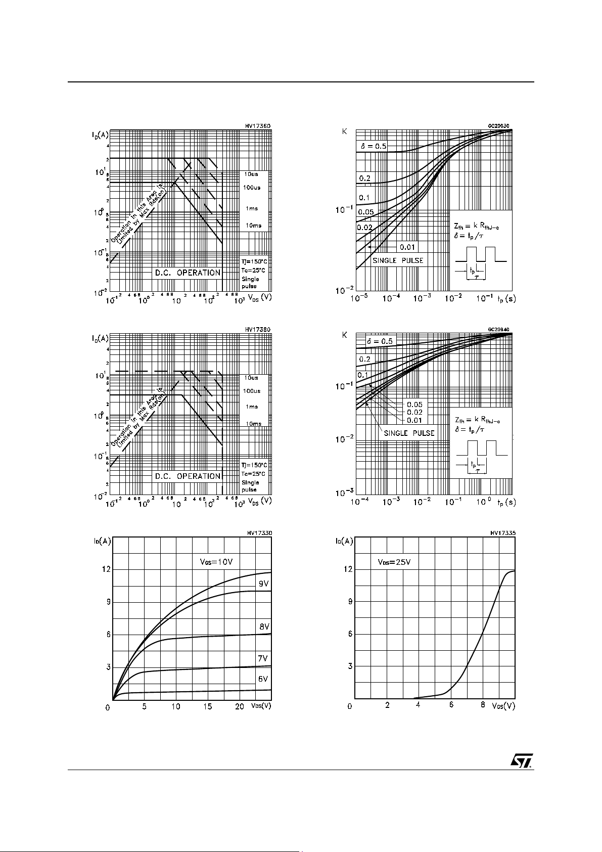
Figure 3: Safe Operating Area for TO-220
Figure 4: Safe Operating Area for TO-220FP
Figure 6: Thermal Impedan ce for TO -2 20
Figure 7: Thermal Impedan ce for TO -2 20FP
Figure 5: Output Characteristics
4/12
Figure 8: Transfer Characteristics
 Loading...