

现货库存、技术资料、百科信息、热点资讯,精彩尽在鼎好!
®
N - CHANNEL 100V - 0.3 Ω - 7A - TO-220
TYPE V
DSS
STP7NE10L 100 V < 0.4 Ω 7 A
■
TYPICAL R
■
EXCEPTIONAL dv/dt CAPABILITY
■
AVALANCHE RUGG ED TECHNOLO GY
■
100 % AVALANCHE TESTED
■
APPLICATION ORIENTED
DS(on)
= 0.3
CHARACTERIZATION
DESCRIPTION
This Power MOSFET is the latest development of
STMicroelectronics unique " Single Feature
Size " strip-based process. The resulting transistor shows extremely high packing density for
low on-resistance, rugged avalanche characteristics and less critical alignment steps therefore
a remarkable manufacturing reproducibility.
APPLICATIONS
■
DC MOTOR CONTROL (DISK DRIVES,etc.)
■
DC-DC & DC-AC CONVERTERS
■
SYNCHRONOU S RECTIFICAT ION
Ω
R
DS(on)
I
D
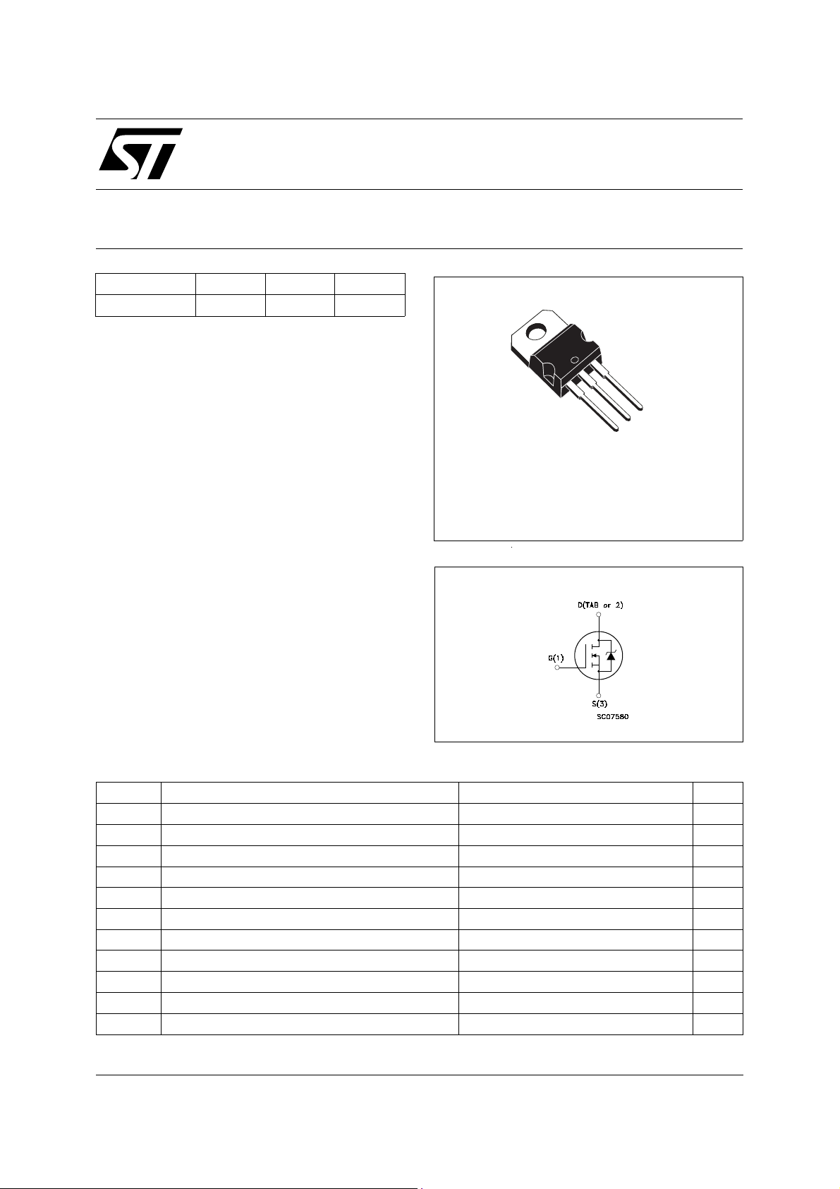
STP7NE10L
STripFET POWER MOSFET
PRELIMINARY DATA
3
2
1
TO-220
INTERNAL SCHEMATIC DIAGRAM
ABSOLUTE MAXIMUM RATINGS
Symbol Parameter Value Unit
V
V
V
I
DM
P
dv/dt(
T
(•) Pulse width limited by safe operating area (1) ISD ≤7 A, di/dt ≤ 200 A/µs, VDD ≤ V
October 1999
Drain-source Voltage (VGS = 0) 10 0 V
DS
Drain- gate Voltage (RGS = 20 kΩ)
DGR
Gate-source Voltage ± 20 V
GS
I
Drain Current (continuous) at Tc = 25 oC7A
D
I
Drain Current (continuous) at Tc = 100 oC4.9A
D
100 V
(•) Drain Current (pulsed) 28 A
Total Dissipation at Tc = 25 oC45W
tot
Derating Factor 0.3 W/
) Peak Diode Recovery voltage slope 6 V/ns
1
Storage Temperature -65 to 150
stg
T
Max. Operating Junction Temperature 175
j
, Tj ≤ T
(BR)DSS
JMAX
o
C
o
C
o
C
1/5
STP7NE10L
THERMAL DATA
R
thj-case
R
thj-amb
R
thc-sink
T
Thermal Resistance Junction-case Max
Thermal Resistance Junction-ambient Max
Thermal Resistance Case-sink Typ
Maximum Lead Temperature For Soldering Purpose
l
AVALANCHE CHARACTERIST ICS
Symbol Parameter Max Value Unit
I
AR
E
Avalanche Current, Repetitive or Not-Repetitive
(pulse width limited by T
Single Pulse Avalanche Energy
AS
(starting T
= 25 oC, ID = IAR, V
j
max)
j
DD
= 30 V)
3.33
100
1.5
275
7A
40 mJ
o
C/W
o
C/W
o
C/W
o
C
ELECTRICAL CHARACTERISTICS
= 25 oC unless otherwise specified)
(T
case
OFF
Symbol Parameter Test Conditions Min. Typ. Max. Unit
V
(BR)DSS
Drain-source
I
= 250 µA V
D
GS
= 0
100 V
Breakdown Voltage
I
DSS
I
GSS
Zero Gate Voltage
Drain Current (V
GS
Gate-body Leakage
Current (V
DS
= 0)
= 0)
= Max Rating
V
DS
V
= Max Rating Tc = 100 oC
DS
V
= ± 20 V
GS
1
10
± 100 nA
ON (∗)
Symbol Parameter Test Conditions Min. Typ. Max. Unit
V
GS(th)
R
DS(on)
I
D(on)
Gate Threshold Voltage
Static Drain-source On
Resistance
V
= VGS ID = 250 µA
DS
V
= 10 V ID = 3.5 A
GS
V
= 5 V ID = 3.5 A
GS
On State Drain Current VDS > I
V
= 10 V
GS
D(on)
x R
DS(on)max
1 1.7 2.5 V
0.3
0.35
7A
0.4
0.45
DYNAMIC
Symbol Parameter Test Conditions Min. Typ. Max. Unit
g
(∗) Forward
fs
Transconductance
C
C
C
Input Capacitance
iss
Output Capacitance
oss
Reverse Transfer
rss
Capacitance
VDS > I
V
DS
x R
D(on)
DS(on)max
= 25 V f = 1 MHz V
ID =2.5 A 2 S
= 0 345
GS
45
20
450
60
25
µA
µA
Ω
Ω
pF
pF
pF
2/5
®
 Loading...