

现货库存、技术资料、百科信息、热点资讯,精彩尽在鼎好!
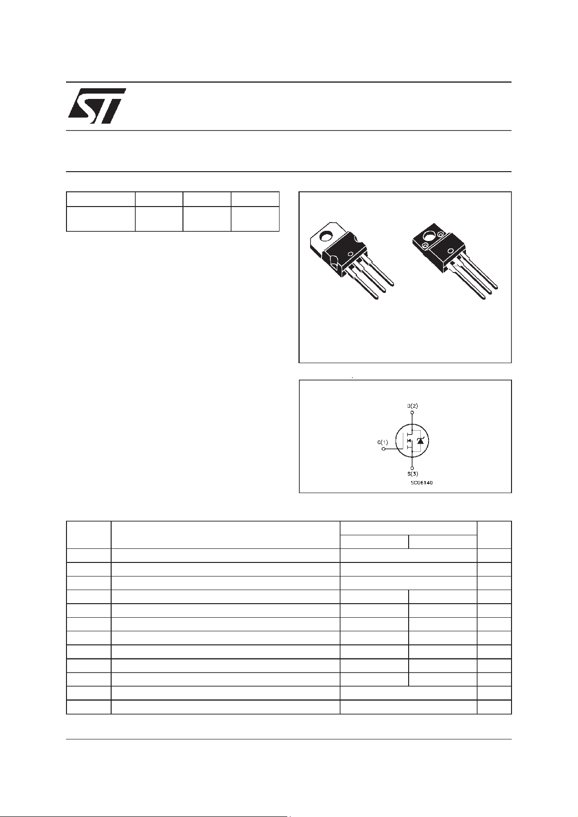
STP7NB30
N - CHANNEL300V - 0.75Ω - 7A - TO-220/TO-220FP
TYPE V
STP7NB30
STP7NB30FP
■ TYPICALR
■ EXTREMELYHIGH dv/dt CAPABILITY
■ 100%AVALANCHETESTED
■ VERYLOW INTRINSIC CAPACITANCES
■ GATECHARGE MINIMIZED
DS(on)
DSS
300 V
300 V
= 0.75
DESCRIPTION
Using the latest high voltage MESH OVERLAY
process, STMicroelectronics has designed an
advanced family of power MOSFETs with
outstanding performances. The new patent
pending strip layout coupled with the Company’s
proprietary edge termination structure, gives the
lowest RDS(on) per area, exceptional avalanche
and dv/dt capabilities and unrivalled gate charge
and switching characteristics.
R
DS(on)
<0.90Ω
<0.90
Ω
Ω
I
D
7A
4A
STP7NB30FP
PowerMESH MOSFET
3
2
1
TO-220 TO-220FP
INTERNAL SCHEMATIC DIAGRAM
3
2
1
APPLICATIONS
■ HIGHCURRENT, HIGHSPEED SWITCHING
■ SWITCHMODE POWER SUPPLIES (SMPS)
■ DC-AC CONVERTERS FOR WELDING
EQUIPMENTANDUNINTERRUPTIBLE
POWERSUPPLIESAND MOTORDRIVE
ABSOLUTE MAXIMUM RATINGS
Symbol Parameter Value Unit
ST P7NB3 0 ST P7NB 30FP
V
V
V
I
DM
P
dv/dt(
V
T
(•) Pulse width limited by safeoperating area (1)ISD≤ 7A, di/dt ≤ 200 A/µs,VDD≤ V
August 1999
Dra in- sour c e Vol t age (VGS= 0) 300 V
DS
Dra in- gate Volt age (RGS=20kΩ)
DGR
Gat e-source Voltage ± 30 V
GS
Dra in Current (c ont in uous ) at Tc=25oC74A
I
D
Dra in Current (c ont in uous ) at Tc=100oC4.42.5A
I
D
300 V
(•) Dra in Current (p ulsed ) 28 28 A
Tot al Dissipation at Tc=25oC8530W
tot
Der ati ng Factor 0.68 0.24 W/
) P eak Di ode Recov er y v olt age slope 5.5 5.5 V/ns
1
Insulation W ithstand Voltage (DC) 2000 V
ISO
St orage Temperatur e -65 t o 150
stg
Max. O perating J unction T emperat ure 150
T
j
,Tj≤T
(BR)DSS
JMAX
o
C
o
C
o
C
1/9
STP7NB30/STP7NB30FP
THERMAL DATA
TO-220 TO-220F P
R
thj-case
R
thj-amb
R
thc-sink
T
AVALANCHE CHARACTERISTICS
Symbol Parameter Max Value Unit
I
AR
E
Ther mal Res istance Junct ion-case Ma x 1.47 4.17
Ther mal Res istance Junct ion-ambient Max
Ther mal Res istance C as e -s ink Ty p
Maximum Lead Te m pe ra t ure For S o lder ing Purp os e
l
Avalanche Current, Repetitive or Not-Repetitive
(pulse width limited by T
Single P ul s e Avalan c he Energy
AS
(starting T
=25oC, ID=IAR,VDD=50V)
j
max)
j
62.5
0.5
300
7A
150 mJ
o
C/W
o
C/W
o
C/W
o
C
ELECTRICAL CHARACTERISTICS
=25oC unless otherwisespecified)
(T
case
OFF
Symbol Parameter Test Conditions Min. Typ. Max. Unit
V
(BR)DSS
Drain-source
=250µAVGS=0
I
D
300 V
Break dow n Volt age
I
DSS
I
GSS
Zero Gate Voltage
Drain Cur rent (V
GS
Gat e- bod y L eak ag e
Current (V
DS
=0)
=0)
V
=MaxRating
DS
=MaxRating Tc=125oC
V
DS
=± 30 V
V
GS
1
10
± 100 nA
ON(∗)
Symbol Parameter Test Conditions Min. Typ. Max. Unit
V
GS(th)
R
DS(on)
Gate Threshold Voltage
Sta t ic Drain -s ource On
V
DS=VGSID
= 250µA
VGS=10V ID= 3.5 A 0.75 0.9 Ω
345V
Resistance
I
D(on)
On State Drain Current VDS>I
D(on)xRDS(on)max
7A
VGS=10V
DYNAMIC
Symbol Parameter Test Conditions Min. Typ. Max. Unit
g
(∗)Forward
fs
Tr ansc on duc tance
C
C
C
Input Capac i t ance
iss
Out put Capacitanc e
oss
Reverse Tr ansfer
rss
Capacit a nc e
VDS>I
D(on)xRDS(on)maxID
=3.5A 1.5 S
VDS=25V f=1MHz VGS= 0 500
100
15
µ
µA
pF
pF
pF
A
2/9
STP7NB30/STP7NB30FP
ELECTRICAL CHARACTERISTICS
(continued)
SWITCHINGON
Symbol Parameter Test Conditions Min. Typ. Max. Unit
t
d(on)
Turn-on Time
t
r
Rise Ti m e
VDD=150V ID= 3.5 A
=4.7 Ω VGS=10V
R
G
13
8
(see test circuit, figure 3)
Q
Q
Q
Tot al Gat e Charge
g
Gat e- Source Charge
gs
Gate-Drain Charge
gd
VDD= 240 V ID=7.0A VGS=10V 17
7.5
6.5
25 nC
SWITCHINGOFF
Symbol Parameter Test Conditions Min. Typ. Max. Unit
t
r(Voff)
t
t
Off-voltage Rise Tim e
Fall T ime
f
Cross-over T ime
c
VDD=240V ID= 7.0 A
=4.7 Ω VGS=10V
R
G
(see test circuit, figure 5)
8
15
7
SOURCEDRAINDIODE
Symbol Parameter Test Conditions Min. Typ. Max. Unit
I
SD
I
SDM
V
SD
t
Q
I
RRM
(∗) Pulsed: Pulse duration = 300 µs, duty cycle 1.5 %
(•) Pulse width limited by safe operatingarea
Source-drain Current
(•)
Source-drain Current
7.0
28
(pulsed)
(∗)ForwardOnVoltage ISD=7.0A VGS=0 1.6 V
Reverse Recovery
rr
Time
Reverse Recovery
rr
= 7.0 A di/dt = 100 A/µs
I
SD
= 100 V Tj=150oC
V
DD
(see test circuit, figure 5)
190
1.1
Charge
Reverse Recovery
11.5
Current
ns
ns
nC
nC
ns
ns
ns
A
A
ns
µ
A
C
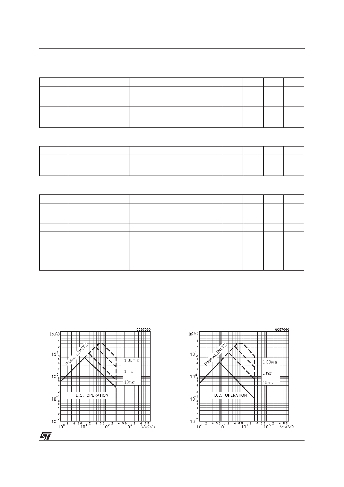
SafeOperating Area for TO-220 SafeOperating Area for TO-220FP
3/9
 Loading...