

ST STP75NF75L, STB75NF75L, STB75NF75L-1 User Manual
现货库存、技术资料、百科信息、热点资讯,精彩尽在鼎好!
STB75NF75L STB75NF75L-1
N-CHANNEL 75V - 0.009 Ω - 75A D2PAK/I2PAK/TO-220
STP75NF75L
STripFET™ II POWER MOSFET
TYPE
STB75NF75L/-1
STP75NF75L
■ TYPICAL R
■ EXCEPTIONA L dv/d t CAPABILITY
■ 100% AVALANCHE TESTED
■ LOW THRESHOLD DRIVE
V
DSS
75 V
75 V
(on) = 0.009Ω
DS
R
DS(on)
<0.011
<0.011
I
D
75 A
Ω
75 A
Ω
DESCRIPTION
This MOSFET series realized with STMicroelectronics
unique STripFET process has specifically been designed
to minimize input capacitance and gate charge. It is
therefore suitable as primary switch in advanced highefficiency, high-frequency isolate d DC-DC c onverters for
Telecom and Computer a pplications. It is also intended
for any applications with low gate drive requirements
.
APPLICATIONS
■ SOLENOID AND RELAY DRIVERS
■ DC MOTOR CONTROL
■ DC-DC CONVERTERS
■ AUTOMOTIVE ENVIRONMENT
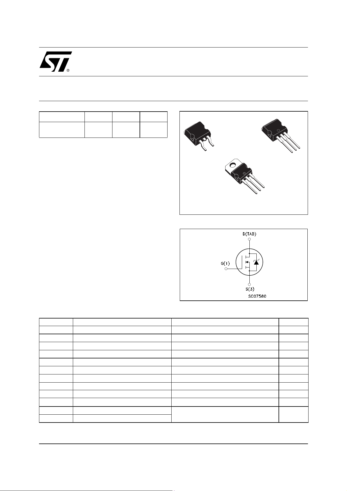
3
1
2
D
PAK
TO-263
3
2
1
TO-220
INTERNAL SCHEMATIC DIAGRAM
2
PAK
I
TO-262
3
2
1
ABSOLUTE MAXIMUM RATINGS
Symbol Parameter Value Unit
V
DS
V
DGR
V
GS
(
I
•)
D
I
D
(
I
••)
DM
P
tot
dv/dt
E
AS
T
stg
T
j
(
Current limited by package
•)
Pulse wi dth limited by safe operating ar ea.
(
••)
.
Drain-source Voltage (VGS = 0)
Drain-gate Voltage (RGS = 20 kΩ)
75 V
75 V
Gate- source Voltage ± 15 V
Drain Current (continuous) at TC = 25°C
Drain Current (continuous) at TC = 100°C
75 A
70 A
Drain Current (pulsed) 300 A
Total Dissipation at TC = 25°C
300 W
Derating Factor 2 W/°C
(1)
Peak Diode Recovery voltage slope 20 V/ns
(2)
Single Pulse Avalanche Energy 680 mJ
Storage Temperature
Max. Operating Junction Temperature
≤ 75A, di/dt ≤ 500A/µs , VDD ≤ V
(1) I
SD
(2) Starting Tj = 25 oC, ID = 37.5A, VDD = 30V
-55 to 175 °C
(BR)DSS
, Tj ≤ T
JMAX.
1/11April 2002
STB75NF75L/-1 STP75NF75L
THERMA L D ATA
Rthj-case
Rthj-amb
T
Thermal Resistance Junction-case
Thermal Resistance Junction-ambient
Maximum Lead Temperature For Soldering Purpose
l
Max
Max
Typ
0.5
62.5
300
°C/W
°C/W
°C
ELECTRICAL CHARACTERISTICS (T
= 25 °C unless otherwise specified)
case
OFF
Symbol Parameter Test Conditions Min. Typ. Max. Unit
I
V
(BR)DSS
Drain-source
= 250 µA VGS = 0
D
75 V
Breakdown Voltage
V
= Max Rating
DS
V
= Max Rating TC = 125°C
DS
V
= ± 15 V
GS
1
10
±100 nA
ON
(*)
I
DSS
I
GSS
Zero Gate Voltage
Drain Current (V
GS
Gate-body Leakage
Current (V
DS
= 0)
= 0)
Symbol Parameter Test Conditions Min. Typ. Max. Unit
V
V
GS(th)
R
DS(on)
Gate Threshold Voltage
Static Drain-source On
Resistance
= VGS I
DS
= 10 V ID = 37.5 A
V
GS
V
= 5 V ID = 37.5 A
GS
= 250 µA
D
1 2.5 V
0.009
0.010
0.011
0.013
DYNAMIC
Symbol Parameter Test Conditions Min. Typ. Max. Unit
(*)
g
fs
Forward Transconductance
15 V ID= 37.5 A
V
DS =
120 S
µA
µA
Ω
Ω
= 25V, f = 1 MHz, VGS = 0
C
iss
C
oss
C
rss
Input Capacitance
Output Capacitance
Reverse Transfer
Capacitance
V
DS
4300
660
205
pF
pF
pF
2/11
STB75NF75L/-1 STP75NF75L
ELECTRICAL CHARACTERISTICS (continued)
SWITCHING ON
Symbol Parameter Test Conditions Min. Typ. Max. Unit
= 40 V ID = 37.5 A
t
d(on)
Turn-on Delay Time
t
r
Rise Time
V
DD
R
= 4.7 Ω VGS = 4.5 V
G
(Resistive Load, Figure 3)
Q
g
Q
gs
Q
gd
Total Gate Charge
Gate-Source Charge
Gate-Drain Charge
= 60V ID = 75 A VGS= 5V
V
DD
SWITCHING OFF
Symbol Parameter Test Conditions Min. Typ. Max. Unit
= 40 V ID = 37.5 A
t
d(off)
Turn-off Delay Time
t
f
Fall Time
V
DD
R
= 4.7Ω, V
G
GS
= 4.5 V
(Resistive Load, Figure 3)
SOURCE DRAIN DIODE
Symbol Parameter Test Conditions Min. Typ. Max. Unit
I
SD
I
SDM
V
SD
t
rr
Q
rr
I
RRM
(*)
Pulsed: P ul se duration = 300 µs, duty cycle 1. 5 %.
(
•)Pulse width limited by safe operating ar ea.
Source-drain Current
(•)
Source-drain Current (pulsed)
(*)
Forward On Voltage
Reverse Recovery Time
Reverse Recovery Charge
Reverse Recovery Current
I
= 75 A VGS = 0
SD
= 75 A di/dt = 100A/µs
I
SD
V
= 20 V Tj = 150°C
DD
(see test circuit, Figure 5)
35
150
75
18
31
110
60
100
380
7.5
90 nC
75
300
1.3 V
ns
ns
nC
nC
ns
ns
A
A
ns
nC
A
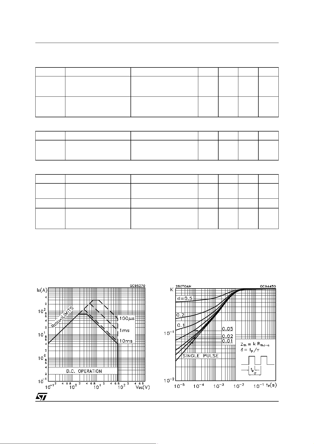
Safe Operating Area Thermal Impedance
3/11
STB75NF75L/-1 STP75NF75L
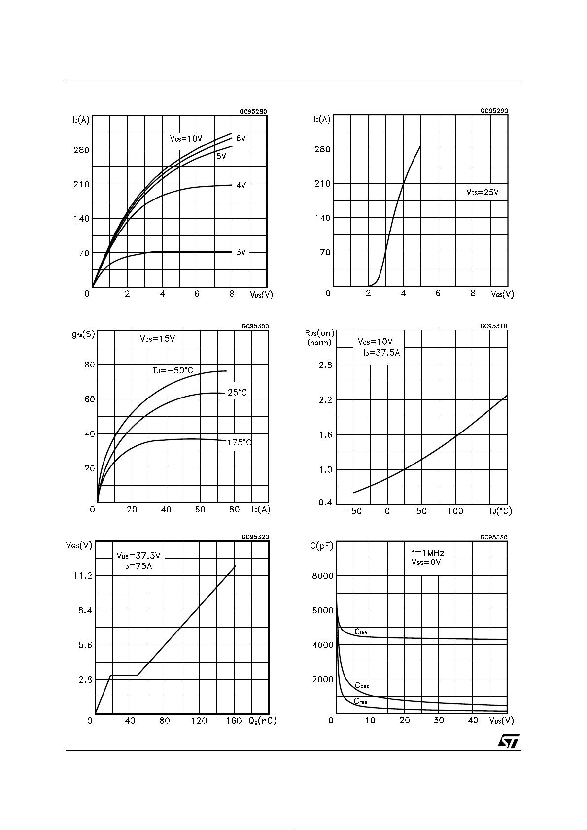
Output Characteristics Transfer Characteristics
Transconductance Static Drain-source On Resistance
Gate Charge vs Gate-source Voltage Capacitance Variations
4/11
 Loading...