

Datasheet STP6NC80ZFP, STP6NC80Z, STB6NC80ZT4, STB6NC80Z-1, STB6NC80Z Datasheet (SGS Thomson Microelectronics)
1/13December 2002
STP6NC80Z - STP6NC80ZFP
STB6NC80Z - STB6NC80Z-1
N-CHANNEL 800V - 1.5Ω - 5.4A TO-220/FP/D²PAK/I²PAK
Zener-Protected PowerMESH™III MOSFET
■ TYPICAL R
DS
(on) = 1.5 Ω
■ EXTREMELY HIGH dv/dtAND CAPABILITY
GATE-TO- SO URCE ZENER DIODES
■ 100% AVALANCHE TESTED
■ V ER Y LOW GATE INPUT RESISTANCE
■ GAT E CHARGE MINIMIZED
DESCRIPTION
The third generation of MESH OVERLAY™ Power
MOSFETs for very high voltage exhibits unsurpassed
on-resistance per unit area while integrating back-toback Zener diodes bet ween gate and source. Such arrangement gives extra ESD capability with higher ruggedness performance as requested b y a large variety
of single-switch applications.
APPLICATIONS
■ S INGLE -ENDED S MPS IN MONITORS,
COMPUTER AND INDUSTRIAL APPLICATION
■ WELDING EQUIPMENT
ABSOLUTE MAXIMUM RATINGS
(•)Pulse width limited by safe operating area
TYPE V
DSS
R
DS(on)
I
D
STP6NC80Z/FP 800V < 1.8 Ω 5.4 A
STB6NC80Z/-1 800V < 1.8 Ω 5.4 A
Symbol Parameter Value Unit
STP(B)6NC80Z(-1) STP6NC80ZFP
V
DS
Drain-source Voltage (VGS=0)
800 V
V
DGR
Drain-gate Voltage (RGS=20kΩ)
800 V
V
GS
Gate- source Voltage ± 25 V
I
D
Drain Current (continuous) at TC= 25°C
5.4 5.4(*) A
I
D
Drain Current (continuous) at TC= 100°C
3.4 3.4(*) A
I
DM
(1)
Drain Current (pulsed) 21 21(*) A
P
TOT
Total Dissipation at TC= 25°C
125 40 W
Derating Factor 1 0.32 W/°C
I
GS
Gate-source Current (●)±50mA
V
ESD(G-S)
Gate source ESD(HBM-C=100pF, R=15KΩ) 3KV
dv/dt Peak Diode Recovery voltage slope 3 V/ns
V
ISO
Insulation Winthstand Voltage (DC) -- 2000 V
T
stg
Storage Temperature –65 to 150 °C
T
j
Max. Operating Junction Temperature 150 °C
(1)ISD≤5.4A,di/dt ≤100A/µs, VDD≤ V
(BR)DSS,Tj≤TJMAX
.
(*)Pulse width Limited by maximum temperature allowed
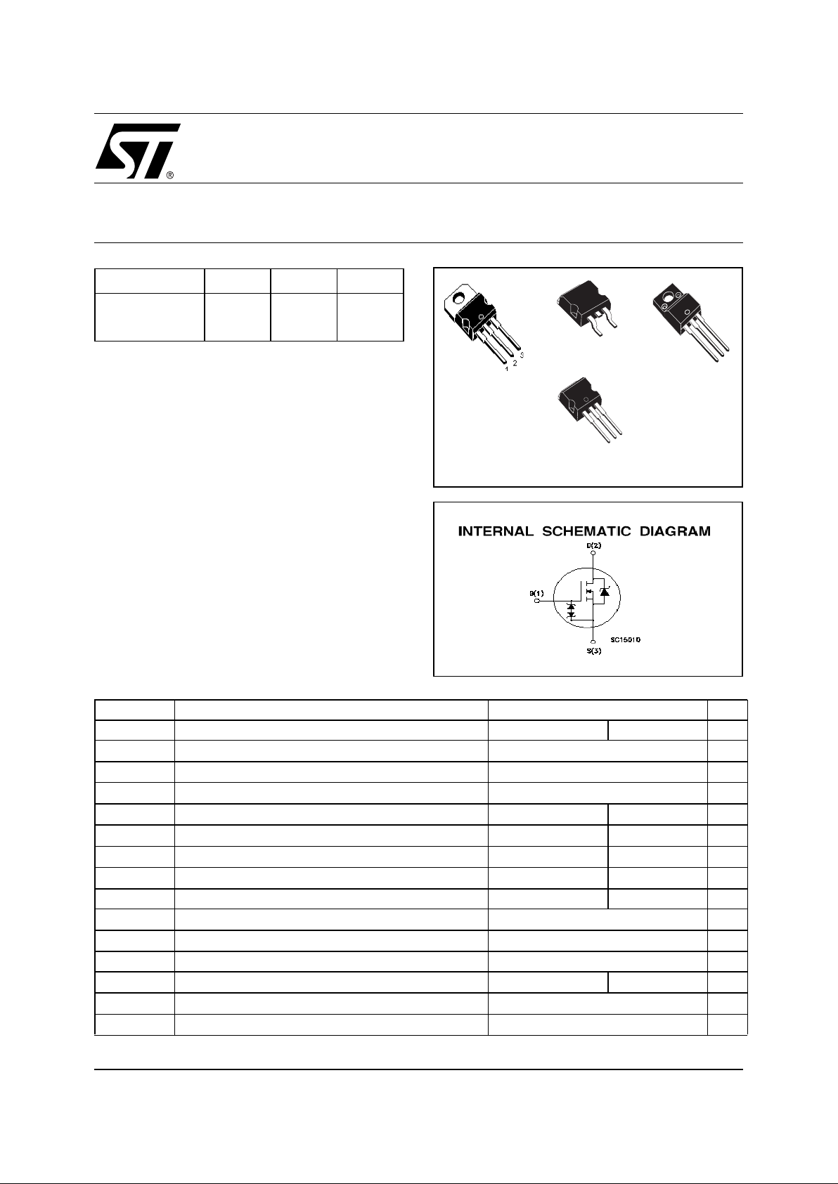
TO-220
1
2
3
TO-220FP
1
2
3
I²PAK
(Tabless TO-220)
1
3
D²PAK

STP6NC80Z/FP/STP6NC80Z-1
2/13
THERMAL DATA
AVALANCHE CHARACTERISTICS
ELECTRICAL CHARACTERISTICS (TCASE = 25 °C UNLESS OTHERWISE SPECIFIED)
OFF
ON (1)
DYNAMIC
TO-220 / D²PAK /
I²PAK
TO-220FP
Rthj-case Thermal Resistance Junction-case Max 1 3.13 °C/W
Rthj-amb Thermal Resistance Junction-ambient Max 30 °C/W
T
l
Maximum Lead Temperature For Soldering Purpose 300 °C
Symbol Parameter Max Value Unit
I
AR
Avalanche Current, Repetitive or Not-Repetitive
(pulse width limited by T
j
max)
5.4 A
E
AS
Single Pulse Avalanche Energy
(starting T
j
= 25 °C, ID=IAR,VDD=50V)
237 mJ
Symbol Parameter Test Conditions Min. Typ. Max. Unit
V
(BR)DSS
Drain-source
Breakdown Voltage
I
D
= 250 µA, VGS=0
800 V
∆BV
DSS
/∆T
J
Breakdown Voltage Temp.
Coefficient
I
D
=1mA,VGS=0
0.9 V/°C
I
DSS
Zero Gate Voltage
Drain Current (V
GS
=0)
V
DS
= Max Rating
1µA
V
DS
= Max Rating, TC= 125 °C
50 µA
I
GSS
Gate-body Leakage
Current (V
DS
=0)
V
GS
= ±20V
±10 µA
Symbol Parameter Test Conditions Min. Typ. Max. Unit
V
GS(th)
Gate Threshold Voltage
V
DS=VGS,ID
= 250µA
345V
R
DS(on)
Static Drain-source On
Resistance
VGS=10V,ID=3A
1.5 1.8 Ω
Symbol Parameter Test Conditions Min. Typ. Max. Unit
g
fs
(1) Forward Transconductance VDS>I
D(on)xRDS(on)max,
ID=3A
7S
C
iss
Input Capacitance
V
DS
=25V,f=1MHz,VGS=0
1600 pF
C
oss
Output Capacitance 125 pF
C
rss
Reverse Transfer
Capacitance
12 pF

3/13
STP6NC80Z/FP/STP6NC80Z-1
ELECTRICAL CHARACTERISTICS (CONTINUED)
SWITCHING ON
SWITCHING OFF
SOURCE DRAIN DIODE
GATE-SOURCE ZENER DIODE
Note: 1. Pulsed: Pulse duration = 300 µs, duty cycle 1.5 %.
2. Pulse width limited by safe operating area.
3. ∆V
BV
= αT(25°-T)BV
GSO
(25°)
PROTECTION FEATURES OF GATE-TO-SOURCE ZENER DIOD ES
The built-in back-to-back Zener diodes have specifically been designed to enhance not only the device’ s
ESD capability, but also t o make them safely absorb possible voltage transients that may occasionally
be applied from gate to source. In this respect the Zen er voltage is ap propriat e to achieve an efficient
and cost-effective intervention to prot ec t the device’s integrity. These integrated Zener diodes thus avoid
the usage of external components.
Symbol Parameter Test Conditions Min. Typ. Max. Unit
t
d(on)
Turn-on Delay Time
V
DD
=400V,ID=3A
RG= 4.7Ω VGS=10V
(see test circuit, Figure 3)
26 ns
t
r
Rise Time 10 ns
Q
g
Total Gate Charge
V
DD
=640V,ID= 6A,
VGS=10V
45 nC
Q
gs
Gate-Source Charge 12 nC
Q
gd
Gate-Drain Charge 18 nC
Symbol Parameter Test Conditions Min. Typ. Max. Unit
t
r(Voff)
Off-voltage Rise Time
V
DD
= 640V, ID=6A,
R
G
=4.7Ω, VGS= 10V
(see test circuit, Figure 5)
11 ns
t
f
Fall Time 13 ns
t
c
Cross-over Time 19 ns
Symbol Parameter Test Conditions Min. Typ. Max. Unit
I
SD
Source-drain Current 5.4 A
I
SDM
(2)
Source-drain Current (pulsed) 21 A
V
SD
(1)
Forward On Voltage
ISD= 5.4 A, VGS=0
1.6 V
t
rr
Reverse Recovery Time
ISD= 6 A, di/dt = 100A/µs,
VDD=50V,Tj= 150°C
(see test circuit, Figure 5)
850 ns
Q
rr
Reverse Recovery Charge 8.1 µC
I
RRM
Reverse Recovery Current 19 A
Symbol Parameter Test Conditions Min. Typ. Max. Unit
BV
GSO
Gate-Source Breakdown
Voltage
Igs=± 1mA (Open Drain) 25 V
αT Voltage Thermal Coefficient T=25°C Note(3) 1.3
10
-4
/°C
Rz Dynamic Resistance
I
D
=50mA,VGS=0
90 Ω
STP6NC80Z/FP/STP6NC80Z-1
4/13
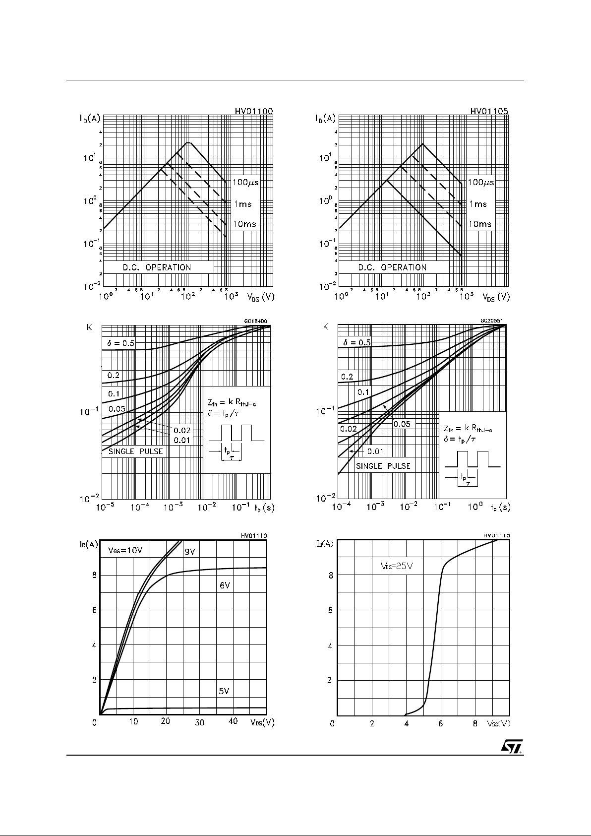
Safe Operating Area For TO-220FPSafe Operating Area For TO-220 /D²PAK/I²PAK
Thermal Impedance For TO-220 /D²PAK/I²PAK
Output Characteristics
Thermal Impedance For TO-220FP
Transfer Characteristics
5/13
STP6NC80Z/FP/STP6NC80Z-1
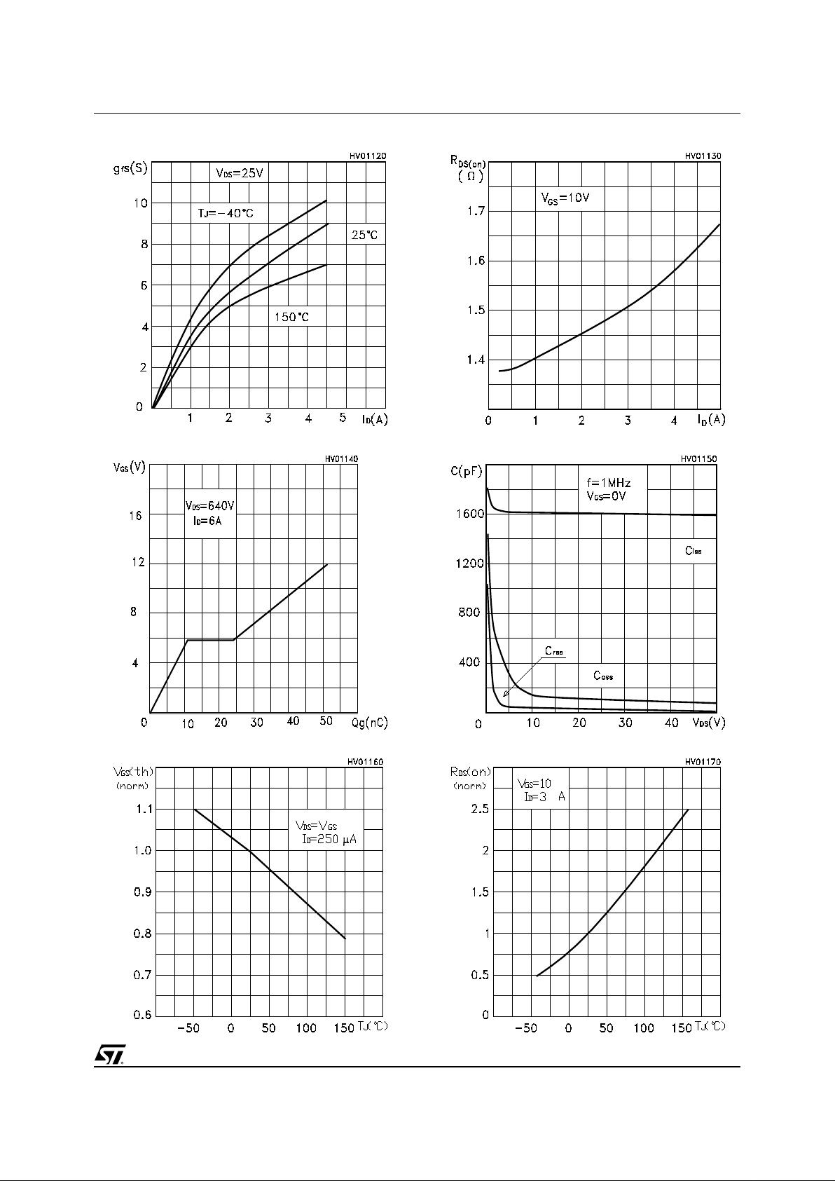
Capacitance Variations
Normalized On Resistance vs TemperatureNormalized Gate Threshold Voltage vs Temp.
Gate Charge vs Gate-source Voltage
Static Drain-source On ResistanceTransconductance
6/13
STP6NC80Z/FP/STP6NC80Z-1
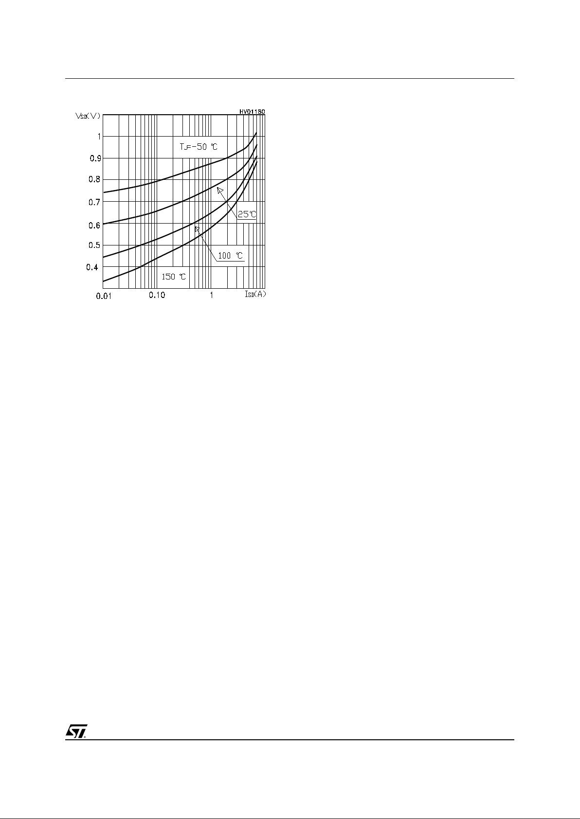
Source-drain Diode Forward Characteristics
7/13
STP6NC80Z/FP/STP6NC80Z-1
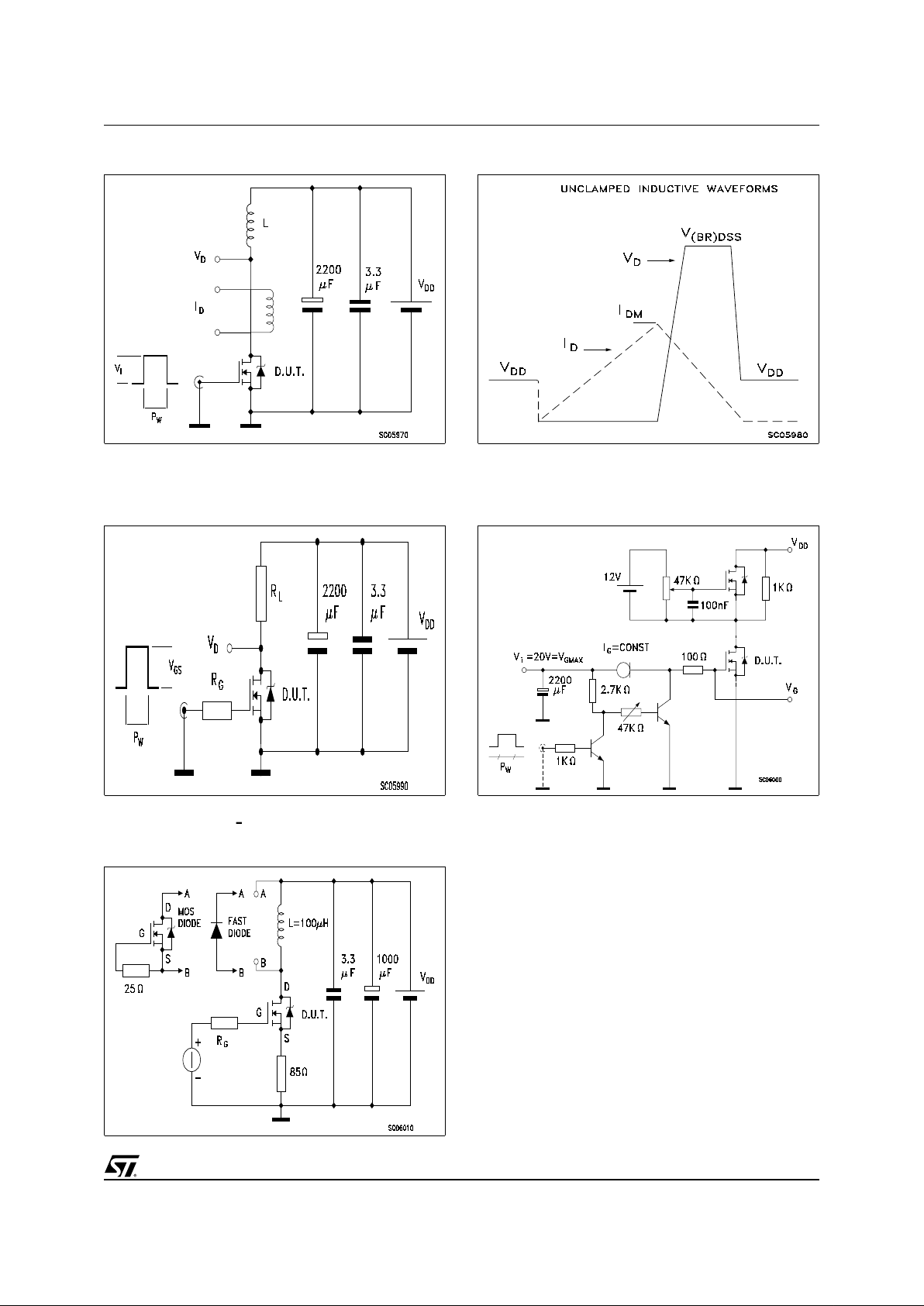
Fig. 5: Test Circuit For Inductive Load Switching
And Di ode Recovery Times
Fig. 4: Gate Charge test Circuit
Fig. 2: Unclamped Inductive WaveformFig. 1: Unclamped Inductive Load Test Circuit
Fig. 3: Switching Times Test Circuits For
Resistive Load
STP6NC80Z/FP/STP6NC80Z-1
8/13
DIM.
mm inch
MIN. TYP. MAX. MIN. TYP. MAX.
A 4.40 4.60 0.173 0.181
C 1.23 1.32 0.048 0.051
D 2.40 2.72 0.094 0.107
D1 1.27 0.050
E 0.49 0.70 0.019 0.027
F 0.61 0.88 0.024 0.034
F1 1.14 1.70 0.044 0.067
F2 1.14 1.70 0.044 0.067
G 4.95 5.15 0.194 0.203
G1 2.4 2.7 0.094 0.106
H2 10.0 10.40 0.393 0.409
L2 16.4 0.645
L4 13.0 14.0 0.511 0.551
L5 2.65 2.95 0.104 0.116
L6 15.25 15.75 0.600 0.620
L7 6.2 6.6 0.244 0.260
L9 3.5 3.93 0.137 0.154
DIA. 3.75 3.85 0.147 0.151
L6
A
C
D
E
D1
F
G
L7
L2
Dia.
F1
L5
L4
H2
L9
F2
G1
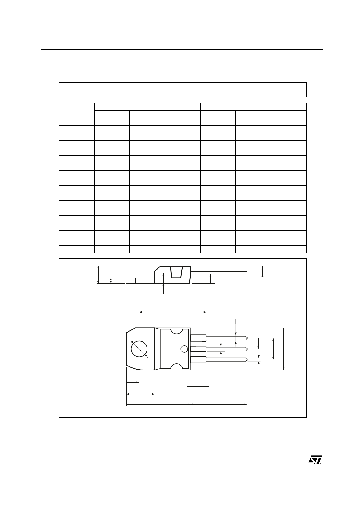
TO-220 MECHANICAL DATA
P011C
9/13
STP6NC80Z/FP/STP6NC80Z-1
DIM.
mm inch
MIN. TYP. MAX. MIN. TYP. MAX.
A 4.4 4.6 0.173 0.181
B 2.5 2.7 0.098 0.106
D 2.5 2.75 0.098 0.108
E 0.45 0.7 0.017 0.027
F 0.75 1 0.030 0.039
F1 1.15 1.7 0.045 0.067
F2 1.15 1.7 0.045 0.067
G 4.95 5.2 0.195 0.204
G1 2.4 2.7 0.094 0.106
H 10 10.4 0.393 0.409
L2 16 0.630
L3 28.6 30.6 1.126 1.204
L4 9.8 10.6 0.385 0.417
L6 15.9 16.4 0.626 0.645
L7 9 9.3 0.354 0.366
Ø 3 3.2 0.118 0.126
L2
A
B
D
E
H
G
L6
¯
F
L3
G1
123
F2
F1
L7
L4
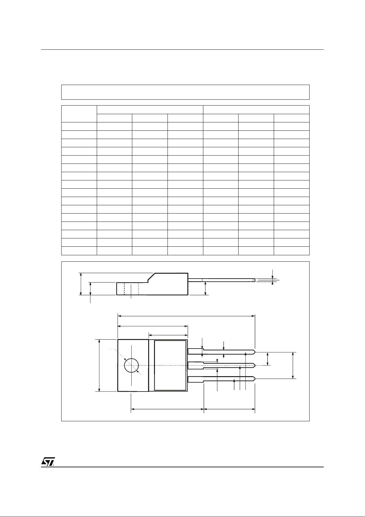
TO-220FP MECHANICAL DAT A

STP6NC80Z/FP/STP6NC80Z-1
10/13
DIM.
mm inch
MIN. TYP. MAX. MIN. TYP. MAX.
A 4.4 4.6 0.173 0.181
A1 2.49 2.69 0.098 0.106
B 0.7 0.93 0.027 0.036
B2 1.14 1.7 0.044 0.067
C 0.45 0.6 0.017 0.023
C2 1.23 1.36 0.048 0.053
D 8.95 9.35 0.352 0.368
e 2.4 2.7 0.094 0.106
E 10 10.4 0.393 0.409
L 13.1 13.6 0.515 0.531
L1 3.48 3.78 0.137 0.149
L2 1.27 1.4 0.050 0.055
L
L1
B2
B
D
E
A
C2
C
A1
L2
e
P011P5/E
TO-262 (I2PAK) MECHANICAL DATA

11/13
STP6NC80Z/FP/STP6NC80Z-1
DIM.
mm inch
MIN. TYP. MAX. MIN. TYP. MAX.
A 4.4 4.6 0.173 0.181
A1 2.49 2.69 0.098 0.106
B 0.7 0.93 0.027 0.036
B2 1.14 1.7 0.044 0.067
C 0.45 0.6 0.017 0.023
C2 1.21 1.36 0.047 0.053
D 8.95 9.35 0.352 0.368
E 10 10.4 0.393 0.409
G 4.88 5.28 0.192 0.208
L 15 15.85 0.590 0.624
L2 1.27 1.4 0.050 0.055
L3 1.4 1.75 0.055 0.068
L2
L3
L
B2
B
G
E
A
C2
D
C
A1
DETAIL "A"
DETAIL "A"
A2
P011P6/E
TO-263 (D2PAK) MECHANICAL DATA

STP6NC80Z/FP/STP6NC80Z-1
12/13
TAPE AND REEL SHIPMENT (suffix ”T4”)*
TUBE SHIPMENT (no suffix)*
D2PAK FOOTPRINT
* on sales type
DIM.
mm inch
MIN. MAX. MIN. MAX.
A 330 12.992
B 1.5 0.059
C 12.8 13.2 0.504 0.520
D 20.2 0795
G 24.4 26.4 0.960 1.039
N 100 3.937
T 30.4 1.197
BASE QTY BULK QTY
1000 1000
REEL MECHANICAL DATA
DIM.
mm inch
MIN. MAX. MIN. MAX.
A0 10.5 10.7 0.413 0.421
B0 15.7 15.9 0.618 0.626
D 1.5 1.6 0.059 0.063
D1 1.59 1.61 0.062 0.063
E 1.65 1.85 0.065 0.073
F 11.4 11.6 0.449 0.456
K0 4.8 5.0 0.189 0.197
P0 3.9 4.1 0. 153 0.161
P1 11.9 12.1 0.468 0.476
P2 1.9 2.1 0. 075 0.082
R 50 1.574
T 0.25 0.35 0.0098 0.0137
W 23.7 24.3 0.933 0.956
TAPE MECHANICAL DATA

STP6NC80Z/FP/STP6NC80Z-1
13/13
Information furnished is believed to be accurate and reliable. However, STMicroelectronics assumes no responsibility f or t he
consequences of use of su ch in formation nor for any in fringement of patents or other rights of third parties w hich may result from
its use. No license is granted by implication or otherwise under any patent or patent rights of STMicroelectronics. Specifications
mentioned in this publication are subject to change without notice. This publication supersedes and replaces all information
previously suppli ed. STMi croelect ronics pr oducts are not author ized for use as cr itical component s in li fe suppo rt devi ces or
systems without express written approval of STMicroelectronics.
© The ST logo is a registered trademark of STMicroelectronics
© 2002 STMicroelectronics - Printed in Italy - All Rights Reserved
STMicroelectronics GROUP OF COMPANIES
Australia - Brazil - Canada - China - Finland - France - Germany - Hong Kong - India - Israel - Italy - Japan - Malaysia - Malta - Morocco
Singapore - Spain - Sweden - Switzerland - United Kingdom - United States.
© http://www.st.com
 Loading...