


STP6NB90
N - CHANNEL 900V - 1.7Ω - 5.8A - TO-220/TO-220FP
TYPE V
STP6NB90
STP6NB90 FP
■ TYPICALR
■ EXTREMELYHIGH dv/dt CAPABILITY
■ 100%AVALANCHETESTED
■ VERYLOW INTRINSIC CAPACITANCES
■ GATECHARGE MINIMIZED
DS(on)
DSS
900 V
900 V
= 1.7
DESCRIPTION
Using the latest high voltage MESH OVERLAY
process, STMicroelectronics has designed an
advanced family of power MOSFETs with
outstanding performances. The new patent
pending strip layout coupled with the Company’s
proprietary edge termination structure, gives the
lowest RDS(on) per area, exceptional avalanche
and dv/dt capabilities and unrivalled gate charge
and switching characteristics.
R
DS(on)
<2 Ω
<2
Ω
I
D
5.8 A
5.8 A
Ω
STP6NB90FP
PowerMESH MOSFET
3
2
1
TO-220 TO-220FP
INTERNAL SCHEMATIC DIAGRAM
3
2
1
APPLICATIONS
■ HIGHCURRENT, HIGHSPEEDSWITCHING
■ SWITCHMODE POWER SUPPLIES(SMPS)
■ DC-AC CONVERTERS FOR WELDING
EQUIPMENTAND UNINTERRUPTIBLE
POWERSUPPLIESAND MOTORDRIVE
ABSOLUTE MAXIMUM RATINGS
Symbol Parameter Value Unit
ST P6 NB90 STP 6NB 90FP
V
V
V
I
DM
P
dv/ dt(
V
T
(•)Pulse width limited by safe operating area (1)I
(*) Limited only by maximum temperature allowed
June 1999
Drain-source Voltage (VGS=0) 900 V
DS
Dra in- gat e Voltage (RGS=20kΩ)
DGR
Gate -sourc e Voltage ± 30 V
GS
Drain Current (continuous) at Tc=25oC5.85.8(*)A
I
D
Drain Current (continuous) at Tc=100oC3.63.6(*)A
I
D
900 V
(•) Drain Current (pulsed) 23 23 A
Total Dissipation at Tc=25oC 135 40 W
tot
Der at in g Fac to r 0.92 0.32 W/
1) P eak Dio de Recove ry voltage slope 4.5 4.5 V/ns
Insulat ion Withst and Voltage (DC) 2000 V
ISO
St orage Temperat ur e -65 to 1 50
stg
Max. Op er a t ing J unctio n Tem pe r at u r e 150
T
j
SD
≤ 6Α,
di/dt≤200A/µs, V
≤
DD
V
(BR)DSS
,Tj≤T
JMAX
o
C
o
C
o
C
1/9

STP6NB90/FP
THERMAL DATA
TO-220 TO220-FP
R
thj-case
R
thj-amb
R
thc-sink
T
AVALANCHE CHARACTERISTICS
Symbol Para meter Max Val ue Uni t
I
AR
E
Ther mal Resis t an ce Junc ti on-cas e Max 1.08 3.13
Ther mal Resis t an ce Junc ti on-ambien t Max
Thermal Resistance Case-sink Typ
Maximum Lead Temper at u r e Fo r Solder ing P ur p ose
l
Avalanche Cu rr ent, Repet it iv e or Not-Repetit iv e
(pulse width limite d by T
Single Pulse Ava lanche Energy
AS
(starting T
=25oC, ID=IAR,VDD=50V)
j
max)
j
62.5
0.5
300
5.8 A
250 mJ
o
C/W
o
C/W
o
C/W
o
C
ELECTRICAL CHARACTERISTICS
=25oC unless otherwisespecified)
(T
case
OFF
Symbol Parameter Test Condit ions Min. Typ. M ax. Unit
V
(BR)DSS
Drain-sourc e
=250µAVGS=0
I
D
900 V
Break d own Voltage
I
DSS
I
GSS
Zero Gate Voltage
Drain C u rr ent (V
GS
Gat e- b ody Le ak a ge
Current (V
DS
=0)
=0)
V
=MaxRating
DS
= Max Rating Tc=125oC
V
DS
=± 30 V
V
GS
1
50
± 100 nA
ON (∗)
Symbol Parameter Test Condit ions Min. Typ. M ax. Unit
V
GS(th)
Gate Threshold
V
DS=VGSID
= 250µA
345V
Voltage
R
DS(on)
Static Drain-source O n
VGS=10V ID=3A 1.7 2 Ω
Resistanc e
I
D(on)
On State Drain Cu rr ent VDS>I
D(on)xRDS(on)max
5.8 A
VGS=10V
DYNAMIC
Symbol Parameter Test Condit ions Min. Typ. M ax. Unit
g
(∗)Forward
fs
Tr ansconduc tance
C
C
C
Input Capacit ance
iss
Out put Capacita nc e
oss
Reverse Tran sfer
rss
Capacitance
VDS>I
D(on)xRDS(on)maxID
=3A 1.5 4 S
VDS=25V f=1MHz VGS= 0 1400
160
18
µ
µA
pF
pF
pF
A
2/9
STP6NB90/FP
ELECTRICAL CHARACTERISTICS
(continued)
SWITCHINGON
Symbol Parameter Test Condit ions Min. Typ. M ax. Unit
t
d(on)
Q
Q
Q
Turn-on delay Time
t
Rise Time
r
Total Gate Charge
g
Gat e- Source Cha r ge
gs
Gate-Drain Charg e
gd
VDD= 450 V ID=3A
=4.7 Ω VGS=10V
R
G
VDD= 720 V ID=6A VGS=10V 40
20
10
55 nC
10
18
SWITCHINGOFF
Symbol Parameter Test Condit ions Min. Typ. M ax. Unit
t
r(Voff)
t
t
Off -voltage Rise Time
Fall Time
f
Cross-ov er T i m e
c
VDD= 720V ID=6A
=4.7 Ω VGS=10V
R
G
15
15
25
SOURCEDRAINDIODE
Symbol Parameter Test Condit ions Min. Typ. M ax. Unit
I
SD
I
SDM
V
SD
t
Q
I
RRM
(∗) Pulsed: Pulse duration = 300 µs, duty cycle 1.5 %
(•) Pulse width limited by safe operatingarea
Source-drain Curr ent
(•)
Source-drain Curr ent
5.8
23
(pulsed)
(∗) For ward On Voltage ISD=5.8 A VGS=0 1.6 V
Reverse Reco v ery
rr
Time
Reverse Reco v ery
rr
= 6 A di/ dt = 100 A/µs
I
SD
= 100 V Tj=150oC
V
DD
650
4.6
Charge
Reverse Reco v ery
14
Current
ns
ns
nC
nC
ns
ns
ns
A
A
ns
µ
A
C
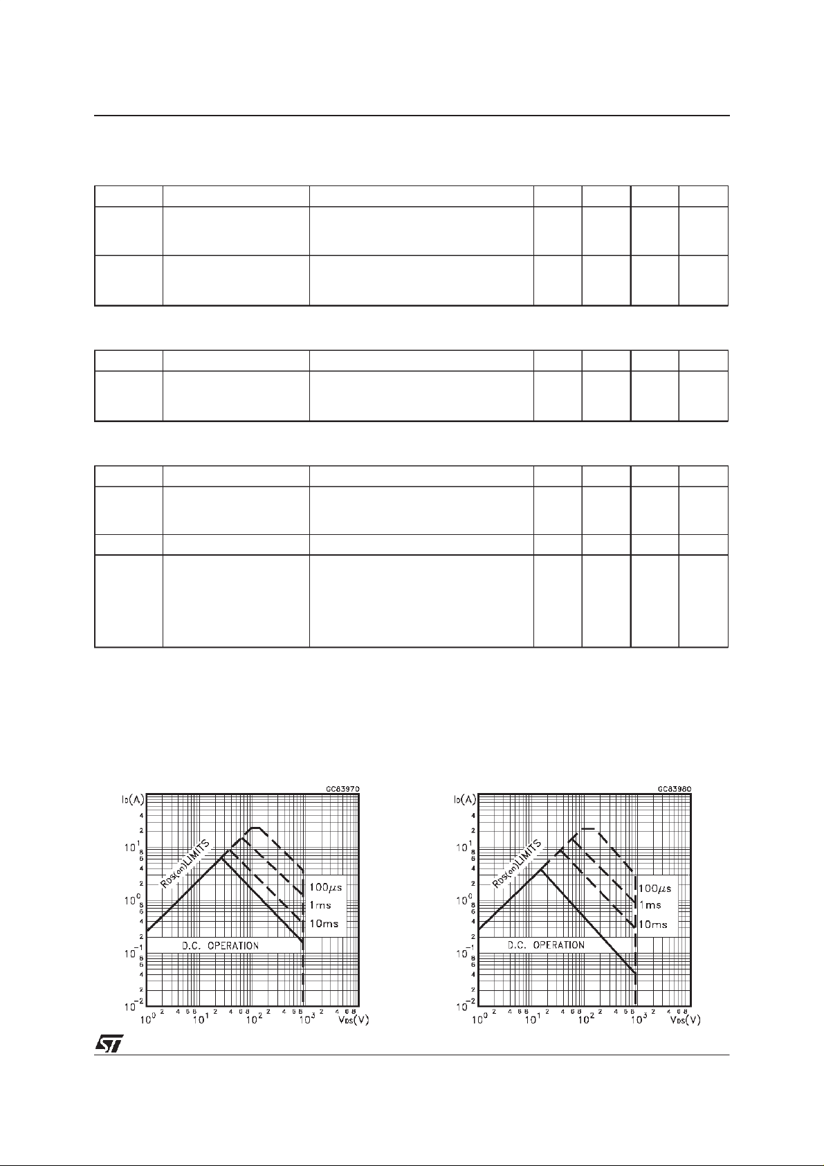
SafeOperating Area for TO-220 SafeOperating Area for TO-220FP
3/9

STP6NB90/FP
ThermalImpedancefor TO-220
OutputCharacteristics
ThermalImpedanceforTO-220FP
TransferCharacteristics
Transconductance
4/9
Static Drain-sourceOn Resistance

STP6NB90/FP
Gate Charge vs Gate-sourceVoltage
Normalized Gate ThresholdVoltage vs
Temperature
CapacitanceVariations
Normalized On Resistance vsTemperature
Source-drainDiode Forward Characteristics
5/9

STP6NB90/FP
Fig. 1: Unclamped InductiveLoad Test Circuit
Fig. 3: Switching Times Test CircuitsFor
ResistiveLoad
Fig. 2: Unclamped InductiveWaveform
Fig. 4: Gate Chargetest Circuit
Fig. 5: Test Circuit For InductiveLoad Switching
And Diode Recovery Times
6/9

TO-220 MECHANICAL DATA
STP6NB90/FP
DIM.
MIN. TYP. MAX. MIN. TYP. MAX.
A 4.40 4.60 0.173 0.181
C 1.23 1.32 0.048 0.051
D 2.40 2.72 0.094 0.107
D1 1.27 0.050
E 0.49 0.70 0.019 0.027
F 0.61 0.88 0.024 0.034
F1 1.14 1.70 0.044 0.067
F2 1.14 1.70 0.044 0.067
G 4.95 5.15 0.194 0.203
G1 2.4 2.7 0.094 0.106
H2 10.0 10.40 0.393 0.409
L2 16.4 0.645
L4 13.0 14.0 0.511 0.551
L5 2.65 2.95 0.104 0.116
L6 15.25 15.75 0.600 0.620
L7 6.2 6.6 0.244 0.260
L9 3.5 3.93 0.137 0.154
DIA. 3.75 3.85 0.147 0.151
mm inch
E
A
L4
D
F2
F1
G1
H2
G
F
P011C
C
D1
L2
Dia.
L5
L7
L6
L9
7/9

STP6NB90/FP
TO-220FP MECHANICAL DATA
DIM.
MIN. TYP. MAX. MIN. TYP. MAX.
A 4.4 4.6 0.173 0.181
B 2.5 2.7 0.098 0.106
D 2.5 2.75 0.098 0.108
E 0.45 0.7 0.017 0.027
F 0.75 1 0.030 0.039
F1 1.15 1.7 0.045 0.067
F2 1.15 1.7 0.045 0.067
G 4.95 5.2 0.195 0.204
G1 2.4 2.7 0.094 0.106
H 10 10.4 0.393 0.409
L2 16 0.630
L3 28.6 30.6 1.126 1.204
L4 9.8 10.6 0.385 0.417
L6 15.9 16.4 0.626 0.645
L7 9 9.3 0.354 0.366
Ø 3 3.2 0.118 0.126
mm inch
E
A
D
B
L3
L6
L7
¯
F1
F
G1
H
G
F2
123
L2
L4
8/9

STP6NB90/FP
Information furnishedis believed tobeaccurateand reliable.However, STMicroelectronics assumes no responsibilityforthe consequences
of use of such information nor for any infringement of patents or other rights of third parties which may result from its use. No license is
granted by implication or otherwise under any patent or patent rights of STMicroelectronics. Specificationmentioned in this publicationare
subjecttochange without notice. This publicationsupersedesandreplaces all information previouslysupplied. STMicroelectronicsproducts
are not authorized for use as critical components in life support devices or systems without express written approval of STMicroelectronics.
The ST logo is a trademark of STMicroelectronics
1999 STMicroelectronics – Printed in Italy – All Rights Reserved
STMicroelectronics GROUP OF COMPANIES
Australia - Brazil - Canada - China - France - Germany - Italy - Japan - Korea - Malaysia - Malta - Mexico - Morocco - The Netherlands -
Singapore - Spain - Sweden - Switzerland - Taiwan- Thailand - United Kingdom - U.S.A.
http://www.st.com
.
9/9
 Loading...