

ST STP5NB80, STP5NB80FP User Manual
查询STP5NB80供应商
STP5NB80
N - CHANNEL 800V - 1.8Ω - 5A - TO-220/TO-220FP
TYPE V
STP5NB80
STP5NB80 FP
■ TYPICALR
■ EXTREMELYHIGH dv/dt CAPABILITY
■ 100%AVALANCHETESTED
■ VERYLOW INTRINSIC CAPACITANCES
■ GATECHARGE MINIMIZED
DS(on)
DSS
800 V
800 V
= 1.8
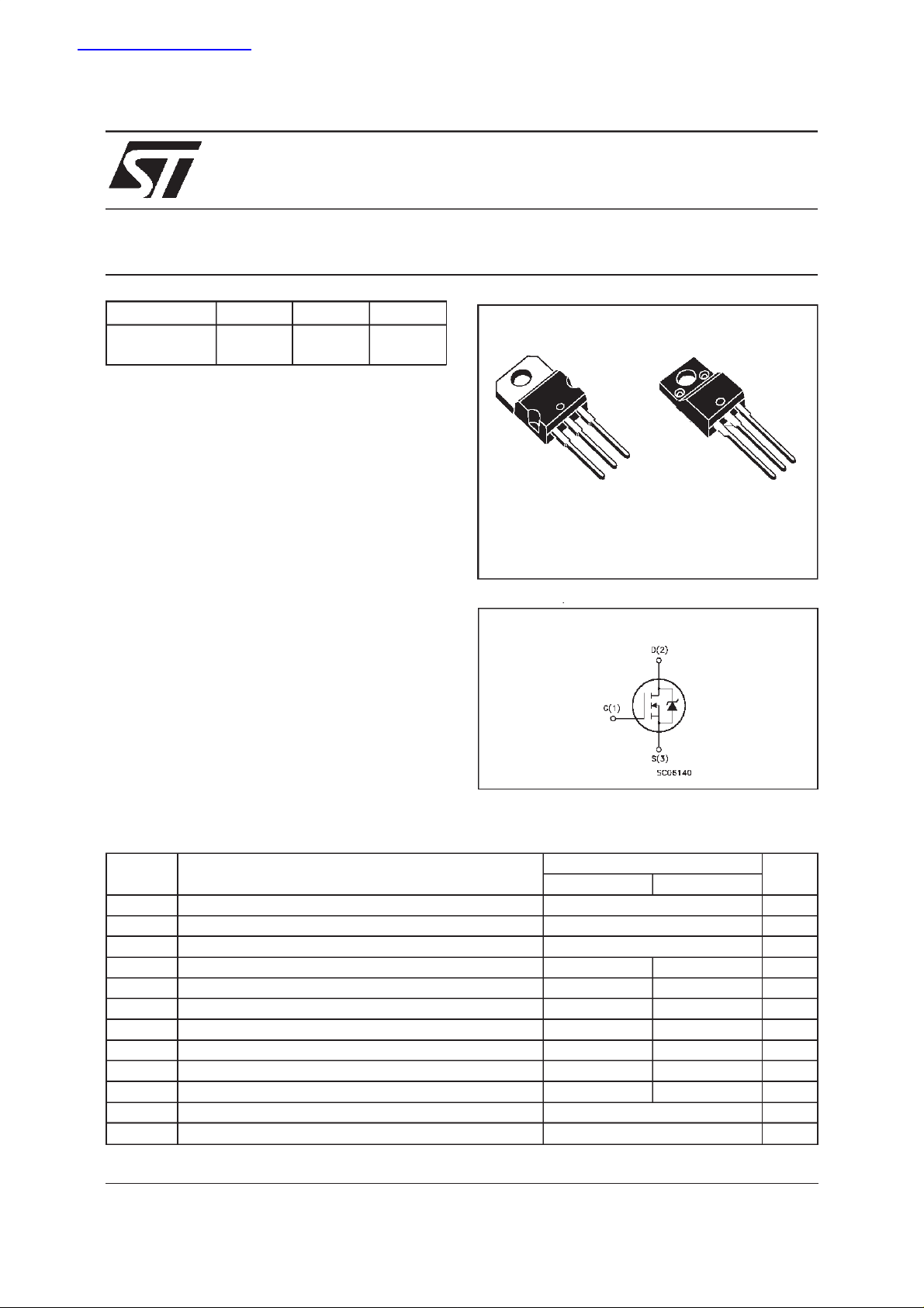
DESCRIPTION
Using the latest high voltageMESH OVERLAY
process, STMicroelectronics has designed an
advanced family of power MOSFETs with
outstanding performances. The new patent
pending strip layout coupled with the Company’s
proprietary edge termination structure, gives the
lowest RDS(on) per area, exceptional avalanche
and dv/dt capabilities and unrivalled gate charge
and switching characteristics.
Ω
R
DS(on)
<2.2Ω
<2.2
Ω
I
D
5A
5A
STP5NB80FP
PowerMESH MOSFET
3
2
1
TO-220 TO-220FP
INTERNAL SCHEMATIC DIAGRAM
3
2
1
APPLICATIONS
■ HIGHCURRENT, HIGHSPEED SWITCHING
■ SWITCHMODE POWER SUPPLIES(SMPS)
■ DC-AC CONVERTERS FOR WELDING
EQUIPMENTAND UNINTERRUPTIBLE
POWERSUPPLIESAND MOTORDRIVE
ABSOLUTE MAXIMUM RATINGS
Symbol Parameter Value Unit
ST P5 NB80 STP 5NB 80FP
V
V
V
I
DM
P
dv/ dt(
V
T
(*) Limited only by maximum temperature allowed (1)ISD≤ 5A, di/dt ≤ 200 A/µs,VDD≤ V
January 1999
Drain-source Voltage ( VGS=0) 800 V
DS
Dra in- gat e Volt a ge (RGS=20kΩ)
DGR
Gate -source V oltage ± 30 V
GS
Dra in Curr en t (c ontinuous) a t Tc=25oC55(*)A
I
D
Dra in Curr en t (c ontinuous) a t Tc= 100oC 3.2 3.2( * ) A
I
D
800 V
(•) Dra in Curr en t (p uls ed) 20 20 A
Tot al Dis s ipation at Tc=25oC 110 40 W
tot
Der at ing Fact or 0.88 0.32 W/
) Peak Diode Recov ery voltag e s lop e 4 4 V/ ns
1
Insulation Withstand Voltage (DC) 2000 V
ISO
St orage Te mpe ra t ure -65 to 150
stg
Max. O perati ng Junction T em p e ra t ure 150
T
j
(BR)DSS
,Tj≤T
JMAX
o
C
o
C
o
C
1/9
STP5NB80/FP
THERMAL DATA
R
thj-case
R
thj-amb
R
thc-sink
T
AVALANCHE CHARACTERISTICS
Ther mal Resis t an ce Junc ti on-cas e Max 1.13 3. 1
Ther mal Resis t an ce Junc ti on-ambien t M a x
Thermal Resistance Case-sink Typ
Maximum Le ad Tem peratu r e F or Sold er ing Purp ose
l
TO-220 TO220-FP
62.5
0.5
300
o
C/W
o
C/W
o
C/W
o
C
Symbol P ara meter Mi n .
I
AR
E
ELECTRICAL CHARACTERISTICS
Avalanche Curr ent, Repetitive or Not- Re petitiv e
(pulse width l imited by T
Single Pu lse Avalanche Energ y
AS
(starting T
=25oC, ID=IAR,VDD=50V)
j
max)
j
(T
case
=25oC unless otherwisespecified)
Value
Max.
Value
5A
300 mJ
OFF
Symbol Parameter Test Conditions Min. Typ. Max. Unit
V
(BR)DSS
Drain-sourc e
=250µAVGS=0
I
D
800 V
Break d own Vo lt age
I
DSS
I
GSS
Zero Gate Voltage
Drain Cu rr ent (V
GS
Gat e- b ody Leakage
Current (V
DS
=0)
=0)
=MaxRating
V
DS
V
= Max Rating Tc=125oC
DS
= ± 30 V
V
GS
1
50
± 100 nA
ON(∗)
Symbol Parameter Test Conditions Min. Typ. Max. Unit
V
GS(th)
R
DS(on)
I
D(on)
Gate Threshold
V
DS=VGSID
Voltage
Static Drain-source O n
VGS=10V ID= 2.5 A 1.8 2.2 Ω
Resistanc e
On St ate Drain Current VDS>I
VGS=10V
= 250 µA
D(on)xRDS(on)max
345V
5A
Unit
µA
A
µ
DYNAMIC
Symbol Parameter Test Conditions Min. Typ. Max. Unit
g
(∗)Forward
fs
C
iss
C
oss
C
rss
2/9
Tr ansconduc tance
Input Cap aci t ance
Out put Capacit ance
Reverse T ransf er
Capacitance
VDS>I
D(on)xRDS(on)maxID
=2.5A 1.5 4 S
VDS=25V f=1MHz VGS= 0 1050
135
15
pF
pF
pF
STP5NB80/FP
ELECTRICAL CHARACTERISTICS
(continued)
SWITCHING ON
Symbol Parameter Test Conditions Min. Typ. Max. Unit
t
d(on)
Turn-on delay Time
t
Rise T im e
r
VDD= 400 V ID=3A
=4.7 Ω VGS=10V
R
G
18
9
(see t est circuit, fi gure 3)
Q
Q
Q
Total Gate Charge
g
Gat e- Source Charge
gs
Gate-Drain Charge
gd
VDD= 480 V ID=5.6A VGS=10V 30
9
14
42 nC
SWITCHING OFF
Symbol Parameter Test Conditions Min. Typ. Max. Unit
t
r(Voff)
t
t
Off -voltage R ise Time
Fall Time
f
Cross-ov er Ti me
c
VDD= 640 V ID=5.6A
=4.7 Ω VGS=10V
R
G
(see t est circuit, fi gure 5)
14
14
21
SOURCEDRAINDIODE
Symbol Parameter Test Conditions Min. Typ. Max. Unit
I
SD
I
SDM
V
SD
t
Q
I
RRM
(∗) Pulsed: Pulse duration = 300 µs, duty cycle 1.5 %
(•) Pulse width limited by safe operatingarea
Source-drain Current
(•)
Source-drain Current
5
20
(pulsed)
(∗) F orwar d O n V oltage ISD=5A VGS=0 1.6 V
Reverse R ecover y
rr
Time
Reverse R ecover y
rr
=5.6A di/dt=100A/µs
I
SD
= 100 V Tj=150oC
V
DD
(see t est circuit, fi gure 5)
700
5
Charge
Reverse R ecover y
14
Current
ns
ns
nC
nC
ns
ns
ns
A
A
ns
µ
A
C
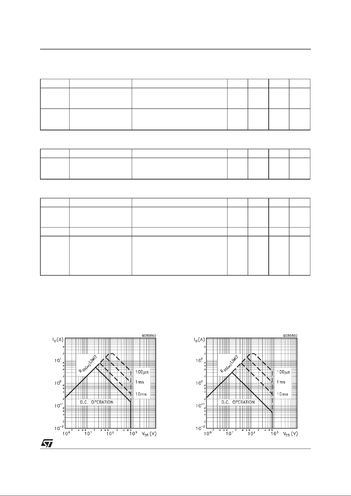
SafeOperating Area for TO-220 SafeOperating Area for TO-220FP
3/9
 Loading...