

STP20NM50FD
STB20NM50FD-1
N-CHANNEL 500V - 0.22Ω -20ATO-220/I2PAK
FDmesh™ Power MOSFET (with FAST DIODE)
TYPE V
STP20NM50FD
STB20NM50FD-1
■ TYPICAL R
■ HIGH dv/dt AND AVALANCHE CAPABILITIES
■ 100% AVALANCHE TESTED
■ LOW INPUT CAPACITANCEAND GATE CHARGE
■ LOW GATE INPUT RESISTANCE
■ TIGHT PROCESS CONTROL AND HIGH
DSSRDS(on)Rds(on)*QgID
500V
500V
(on) = 0.22Ω
DS
<0.25Ω
<0.25Ω
8.36 Ω*nC
8.36 Ω*nC
20 A
20 A
MANUFACTURING YIELDS
DESCRIPTION
The FDmesh™ associates all advantages of red uc ed
on-resistance and fast switching with an intrinsic fa strecovery body diode. I t is therefore strongly recommended forbridge to pologies,in particularZVS phaseshift converters.
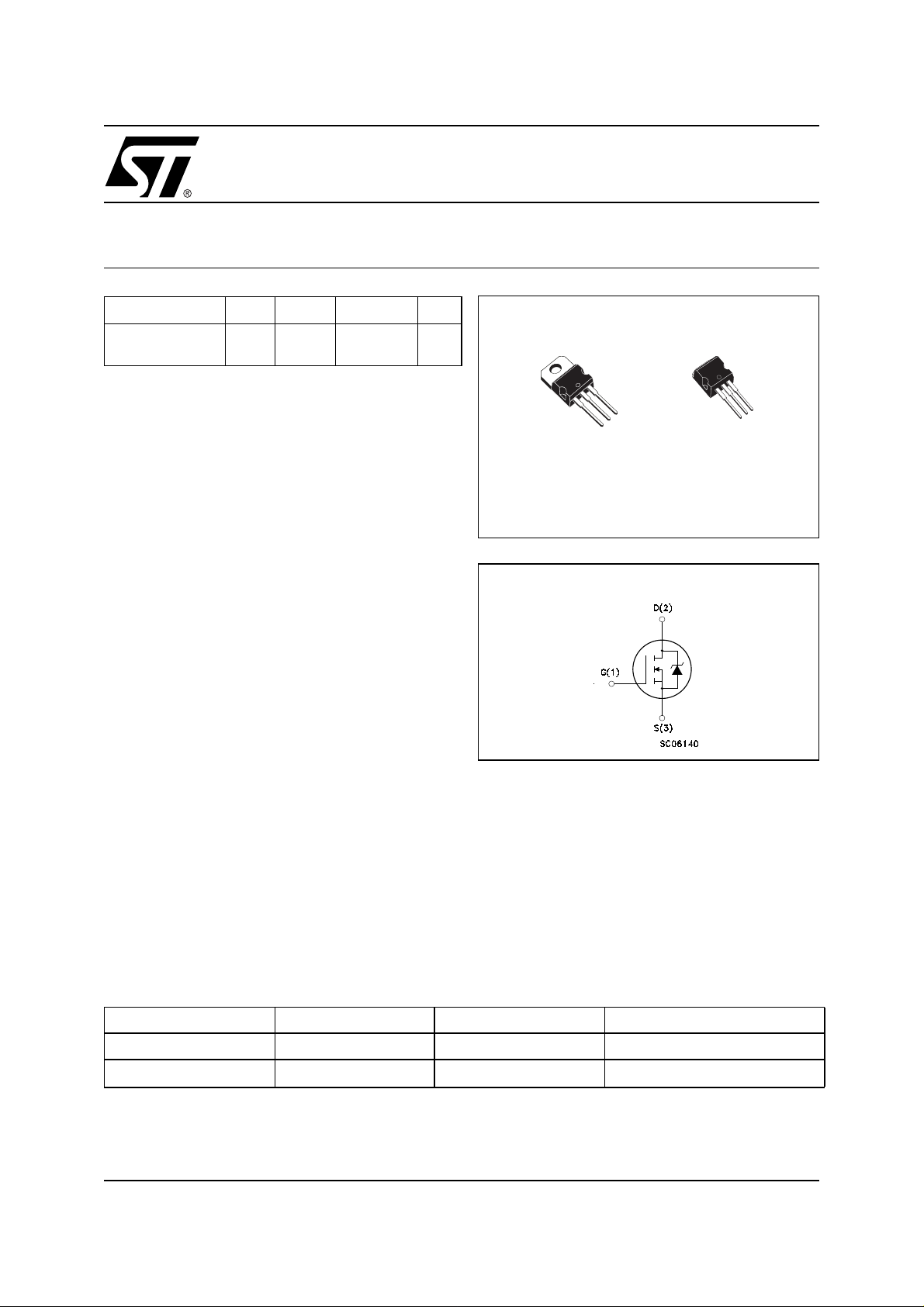
3
2
1
TO-220
I
NTERNAL SCHEMATIC DIAGRAM
I2PAK
(Tabless TO-220)
3
2
1
APPLICATIONS
■ ZVSPHASE-SHIFTFULLBRIDGECONVERTERS
FOR SMPS AND WELDING EQUIPMENT
ORDERING INFORMATION
SALES TYPE MARKING PACKAGE PACKAGING
STP20NM50FD P20NM50FD TO-220 TUBE
STB20NM50FD-1 B20NM50FD-1
I
2
PAK
TUBE
1/9August 2003

STP20NM50FD/STB20NM50FD- 1
ABSOLUTE MAXIMUM RATINGS
Symbol Parameter Value Unit
V
DS
V
DGR
V
GS
I
D
I
D
I
DM
P
TOT
dv/dt (1) Peak Diode Recovery voltage slope 20 V/ns
T
stg
T
j
() Pulse width limited by safe operating area
≤ 20A,di/dt≤ 200 A/µs, VDD≤ V
(1) I
SD
THERMAL DATA
Rthj-case Thermal Resistance Junction-case Max 0.65 °C/W
Rthj-amb Thermal Resistance Junction-ambient Max 62.5 °C/W
T
l
Drain-source Voltage (VGS=0)
Drain-gate Voltage (RGS=20kΩ)
500 V
500 V
Gate- source Voltage ±30 V
Drain Current (continuous) at TC= 25°C
Drain Current (continuous) at TC= 100°C
()
Drain Current (pulsed) 80 A
Total Dissipation at TC= 25°C
20 A
14 A
192 W
Derating Factor 1.2 W/°C
Storage Temperature –65 to 150 °C
Max. Operating Junction Temperature 150 °C
(BR)DSS,Tj≤TJMAX.
Maximum Lead Temperature For Soldering Purpose 300 °C
AVALANCHE CHARACTERISTICS
Symbol Parameter Max Value Unit
I
AR
E
AS
Avalanche Current, Repetitive or Not-Repetitive
(pulse width limited by T
max)
j
Single Pulse Avalanche Energy
(starting T
= 25 °C, ID=IAR,VDD=35V)
j
10 A
700 mJ
ELECTRICAL CHARACTERISTICS (TCASE = 25 °C UNLESS OTHERWISE SPECIFIED)
ON/OFF
Symbol Parameter Test Conditions Min. Typ. Max. Unit
V
(BR)DSS
I
DSS
I
GSS
V
GS(th
R
DS(on)
Drain-source
Breakdown Voltage
Zero Gate Voltage
Drain Current (V
GS
=0)
Gate-body Leakage
Current (V
DS
=0)
Gate Threshold Voltage
Static Drain-source On
Resistance
ID= 250 µA, VGS=0 500 V
V
= Max Rating
DS
= Max Rating, TC= 125 °C
V
DS
V
= ±30V ±100 nA
GS
V
DS=VGS,ID
= 250 µA
34
1µA
10 µA
5V
VGS= 10V, ID= 10A 0.22 0.25 Ω
2/9
STP20NM50FD/STB20NM50FD-1
ELECTRICAL CHARACTERISTICS (CONTINUED)
DYNAMIC
Symbol Parameter Test Conditions Min. Typ. Max. Unit
(1) Forward Transconductance VDS>I
g
fs
D(on)xRDS(on)max,
ID= 10A
C
iss
C
oss
C
rss
C
oss eq.
Input Capacitance
Output Capacitance
Reverse Transfer
Capacitance
(2) Equivalent Output
=25V,f=1MHz,VGS= 0 1380
V
DS
VGS=0V,VDS= 0V to 400V 130 pF
Capacitance
R
g
Gate Input Resistance f=1 MHz Gate DC Bias=0
Test Signal Level=20mV
Open Drain
(1) Pulsed: Pulse duration = 300 µs, duty cycle 1.5 %.
(2) C
is defined as a constant equivalent capacitance giving the same charging time as C
oss eq.
when VDSincreases from 0 to 80% V
oss
SWITCHING ON
Symbol Parameter Test Conditions Min. Typ. Max. Unit
V
t
d(on)
Q
Q
Q
Turn-on Delay Time
t
r
g
gs
gd
Rise Time 20 ns
Total Gate Charge
Gate-Source Charge
Gate-Drain Charge
=250V,ID=10A
DD
RG= 4.7Ω VGS=10V
(see test circuit, Figure 3)
VDD=400V,ID= 20A,
V
=10V
GS
9S
290
40
2.8 Ω
22 ns
38
53 nC
18
10
pF
pF
pF
nC
nC
DSS
.
SWITCHING OFF
Symbol Parameter Test Conditions Min. Typ. Max. Unit
V
t
r(Voff)
t
f
t
c
Off-voltage Rise Time
Fall Time 15 ns
Cross-over Time 30 ns
= 400V, ID=20A,
DD
R
=4.7Ω, VGS= 10V
G
(see test circuit, Figure 5)
6ns
SOURCE DRAIN DIODE
Symbol Parameter Test Conditions Min. Typ. Max. Unit
I
SD
I
SDM
VSD(1)
t
rr
Q
rr
I
RRM
Note: 1. Pulsed: Pulse duration = 300 µs, duty cycle 1.5 %.
2. Pulse width limited by safe operating area.
Source-drain Current 20 A
(2)
Source-drain Current (pulsed) 80 A
Forward On Voltage
Reverse Recovery Time
Reverse Recovery Charge 2 µC
ISD=20A,VGS=0
I
= 20 A, di/dt = 100A/µs,
SD
=60V,Tj= 150°C
V
DD
(see test circuit, Figure 5)
245 ns
Reverse Recovery Current 16 A
1.5 V
3/9

STP20NM50FD/STB20NM50FD- 1
Safe Operating A rea For TO-220 / I²PAK Thermal Impedance For TO-220 / I²PA K
Output Characteristics
Transconductance
Transfer Characteristics
Static Drain-source On Resistance
4/9

STP20NM50FD/STB20NM50FD-1
Gate Charge vs Gate-so urce Voltage
Capacitance Variations
Normalized On Resistance vs TemperatureNormalized Gate Theresho ld Voltage vs Temp.
Source-drain Diode Forward Characteristics
5/9

STP20NM50FD/STB20NM50FD- 1
Fig. 2: Unclamped Inductive WaveformFig. 1: Unclamped Inductive Load Test Circuit
Fig. 3: Switching Times Test Circuit For
Resistive Load
Fig. 5: Test Circuit For Induc tiv e Load Switching
And Diode Recovery Times
Fig. 4: Gate Charge test Circuit
6/9

STP20NM50FD/STB20NM50FD-1
TO-220 MECHANICAL DATA
DIM.
A 4.40 4.60 0.173 0.181
b 0.61 0.88 0.024 0.034
b1 1.15 1.70 0.045 0.066
c 0.49 0.70 0.019 0.027
D 15.25 15.75 0.60 0.620
E 10 10.40 0.393 0.409
e 2.40 2.70 0.094 0.106
e1 4.95 5.15 0.194 0.202
F 1.23 1.32 0.048 0.052
H1 6.20 6.60 0.244 0.256
J1 2.40 2.72 0.094 0.107
L 13 14 0.511 0.551
L1 3.50 3.93 0.137 0.154
L20 16.40 0.645
L30 28.90 1.137
øP 3.75 3.85 0.147 0.151
Q 2.65 2.95 0.104 0.116
MIN. TYP MAX. MIN. TYP. MAX.
mm. inch
7/9

STP20NM50FD/STB20NM50FD- 1
TO-262 (I2PAK) MECHANICAL DATA
DIM.
A 4.40 4.60 0.173 0.181
A1 2.40 2.72 0.094 0.107
b 0.61 0.88 0.024 0.034
b1 1.14 1.70 0.044 0.066
c 0.49 0.70 0.019 0.027
c2 1.23 1.32 0.048 0.052
D 8.95 9.35 0.352 0.368
e 2.40 2.70 0.094 0.106
e1 4.95 5.15 0.194 0.202
E 10 10.40 0.393 0.410
L 13 14 0.511 0.551
L1 3.50 3.93 0.137 0.154
L2 1.27 1.40 0.050 0.055
MIN. TYP MAX. MIN. TYP. MAX.
mm. inch
8/9

STP20NM50FD/STB20NM50FD-1
Information furnished is believed to be accurate and reliable. However, STMicroelectronics assumes no responsibility for the
consequences of u se of such inf ormat ion nor for any in fring ement of p aten ts or othe r ri ghts of th ird p arties whic h may resul t f rom
its use. No license is granted by implication or otherwise under any patent or patent rights of STMicroelectronics. Specifications
mentioned in this publication are subject to change without notice. This publication supersedes and replaces all information
previously supplied. STMicroelectronics products are not authorized for use as critical components in life support devices or
systems without express written approval of STMicroelectronics.
Australia - Brazil - Canada - China - Finland - France - Germany - Hong Kong - India - Israel - Italy - Japan - Malaysia - Malta - Morocco
© The ST logo is a registered trademark of STMicroelectronics
© 2003 STMicroelectronics - Printed in Italy - All Rights Reserved
Singapore - Spain - Sweden - Switzerland - United Kingdom - United States.
STMicroelectronics GROUP OF COMPANIES
© http://www.st.com
9/9
 Loading...