

ST STP20NE06, STP20NE06FP User Manual
查询STP20NE06供应商
STP20NE06
N - CHANNEL 60V - 0.06 Ω - 20A TO-220/TO-220FP
TYPE V
ST P20NE06
ST P20NE06FP
■ TYPICALR
■ EXCEPTIONALdv/dtCAPABILITY
■ 100%AVALANCHETESTED
■ LOW GATE CHARGE 100
■ APPLICATIONORIENTED
DS(on)
DSS
60 V
60 V
= 0.06 Ω
CHARACTERIZATION
DESCRIPTION
This Power Mosfet is the latest development of
STMicroelectronics unique ” Single Feature
Size ” strip-basedprocess. The resulting transi-
stor shows extremelyhigh packing densityforlow
on-resistance, rugged avalance characteristics
and less critical alignment steps therefore a remarkablemanufacturingreproducibility.
R
DS(on)
<0.080Ω
<0.080Ω
o
C
I
D
20 A
13 A
STP20NE06FP
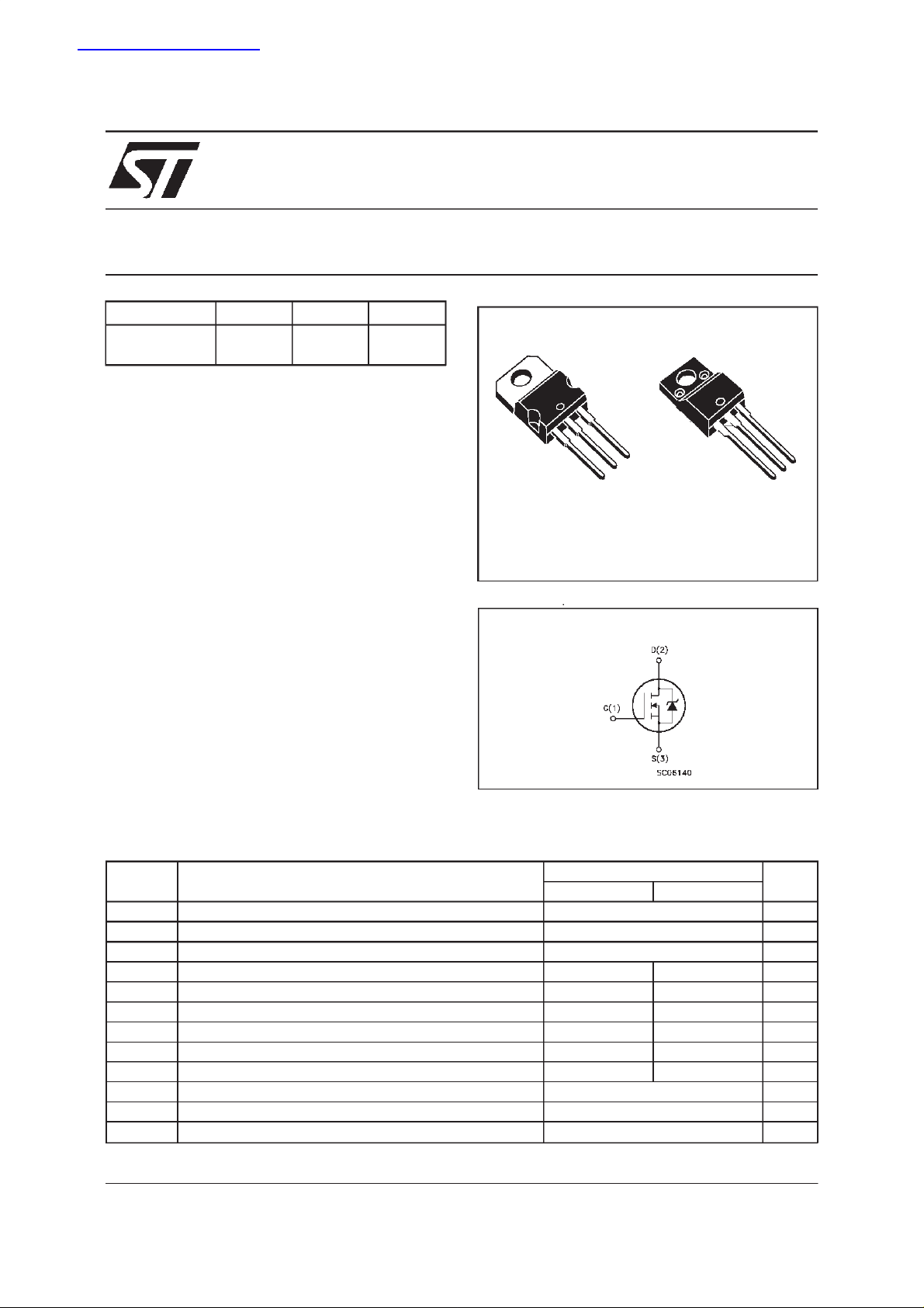
STripFET POWER MOSFET
3
2
1
TO-220 TO-220FP
INTERNAL SCHEMATIC DIAGRAM
3
2
1
APPLICATIONS
■ HIGHCURRENT, HIGH SPEEDSWITCHING
■ SOLENOIDAND RELAY DRIVERS
■ MOTORCONTROL, AUDIOAMPLIFIERS
■ DC-DC& DC-AC CONVERTERS
■ AUTOMOTIVEENVIRONMENT(INJECTION,
ABS, AIR-BAG, LAMPDRIVERS,Etc.)
ABSOLUTE MAXIMUM RATINGS
Symbol Parameter Value Unit
ST P20NE06 STP20NE06FP
V
V
V
I
DM
P
V
dv/ dt P ea k Diode Recover y volt age slope 7 V/ ns
T
(•) Pulse width limited by safe operating area (1)ISD≤ 20 A, di/dt ≤ 300 A/µs, VDD≤ V
June 1999
Drain-source Voltage (VGS=0) 60 V
DS
Drain- gate Vol t age (RGS=20kΩ)60V
DGR
Gate-source Voltage ± 20 V
GS
I
Drain Curre nt (cont i nuous) at Tc=25oC2013A
D
Drain Curre nt (cont i nuous) at Tc=100oC149A
I
D
(•) Drain Curre nt (pulse d) 80 80 A
Total Dissipation at Tc=25oC7030W
tot
Derat ing F ac tor 0.47 0.2 W/
Ins ulat ion W i th s t and Voltage ( DC) 2000 V
ISO
Sto rage Temper at ur e -65 to 175
stg
T
Max. Operat ing Junct ion Tem pe ra ture 175
j
(BR)DSS,Tj≤TJMAX
o
C
o
C
o
C
1/9
STP20NE06/FP
THERMAL DATA
TO-220 TO-220FP
R
thj-case
R
thj-amb
R
thc-sink
T
AVALANCHE CHARACTERISTICS
Symbol Parameter Max V alue Unit
I
AR
E
Ther mal Resistanc e Junct ion-case M a x 2.14 5
Ther mal Resistanc e Junct ion-ambie nt Max
Ther mal Resistanc e Case-sink Ty p
Maximum Lead Tempe ra tur e F or S o ldering Purpos e
l
Avalanche Current, R epetitive or Not-Repetitive
(pulse width limited by T
Single Pul se Avalanc he Ener gy
AS
(starting T
=25oC, ID=IAR,VDD=25V)
j
max)
j
62.5
0.5
300
20 A
100 mJ
o
C/W
o
C/W
o
C/W
o
C
ELECTRICAL CHARACTERISTICS
=25oC unless otherwisespecified)
(T
case
OFF
Symbol Parameter Test Conditions Min. Typ. Max. Unit
V
(BR)DSS
Drain-source
ID=250µAVGS=0 60 V
Break dow n Vo lt age
I
DSS
I
GSS
Zero Gate Volta ge
Drain Curre nt (V
GS
Gat e- bod y Leakag e
Current (V
DS
=0)
=0)
V
=MaxRating
DS
=MaxRating Tc= 125oC
V
DS
V
=± 20 V
GS
1
10
100 nA
±
ON(∗)
Symbol Parameter Test Conditions Min. Typ. Max. Unit
V
GS(th)
R
DS(on)
Gate Threshold Voltage VDS=VGSID= 250µA 234V
Sta t ic Drain-s our c e On
VGS=10V ID= 10 A 0.060 0.080
Resistance
I
D(on)
On State Drain Current VDS>I
D(on)xRDS(on)max
20 A
VGS=10V
DYNAMIC
Symbol Parameter Test Conditions Min. Typ. Max. Unit
g
(∗)Forward
fs
Tr ansc on duc tance
C
C
C
Input Capaci t ance
iss
Out put Capac itance
oss
Reverse Transfer
rss
Capacit a nc e
VDS>I
D(on)xRDS(on)maxID
=10 A 5 9 S
VDS=25V f=1MHz VGS= 0 900
125
35
µA
µA
Ω
pF
pF
pF
2/9
STP20NE06/FP
ELECTRICAL CHARACTERISTICS
(continued)
SWITCHING ON
Symbol Parameter Test Conditions Min. Typ. Max. Unit
t
d(on)
t
Tur n-on Delay T ime
Rise Time
r
VDD=30V ID=10A
R
G
=4.7
Ω
VGS=10V
20
45
(see test circuit, figure 3)
Q
Q
Q
Tot al Gate Charge
g
Gat e- Source Charg e
gs
Gate-Drain Charge
gd
VDD=48V ID=20A VGS=10V 25
10
6
35 nC
SWITCHING OFF
Symbol Parameter Test Conditions Min. Typ. Max. Unit
t
r(Voff)
t
t
Off-v oltage Rise Time
Fall T ime
f
Cross-over T im e
c
VDD=48V ID=20A
=4.7 Ω VGS=10V
R
G
(see test circuit, figure 5)
8
25
37
SOURCEDRAINDIODE
Symbol Parameter Test Conditions Min. Typ. Max. Unit
I
SD
I
SDM
V
SD
t
Q
I
RRM
(∗) Pulsed:Pulse duration= 300µs, duty cycle 1.5%
(•) Pulse width limited by safe operatingarea
Source-drain Current
(•)
Source-drain Current
20
80
(pulsed)
(∗)ForwardOnVoltage ISD=20A VGS=0 1.5 V
Reverse Recovery
rr
Time
Reverse Recovery
rr
ISD= 20 A di/dt = 100 A/µs
=30V Tj= 150oC
V
DD
(see test circuit, figure 5)
50
115
Charge
Reverse Recovery
4.5
Current
ns
ns
nC
nC
ns
ns
ns
A
A
ns
nC
A
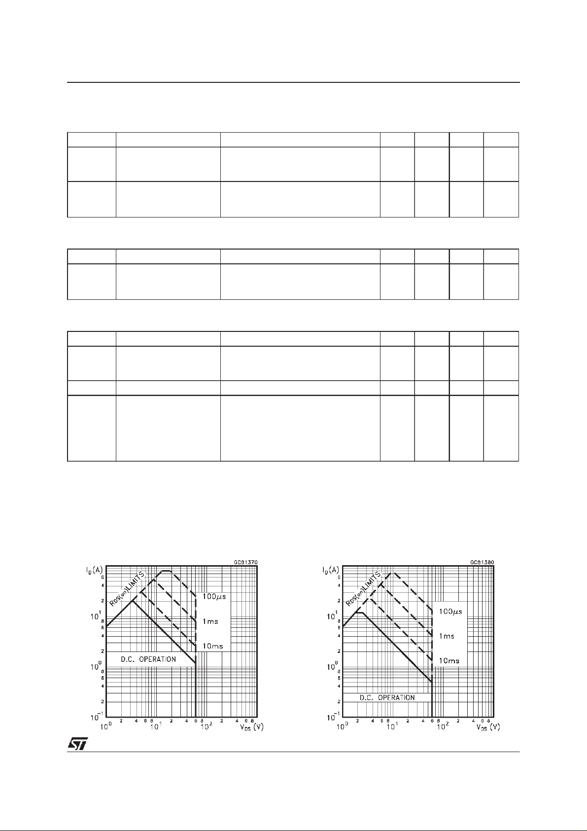
SafeOperating Area for TO-220 SafeOperating Area for TO-220FP
3/9
 Loading...