


查询STP19N06L供应商
LOW THRESHOLD POWER MOS TRANSISTOR
STP19N06L
STP19N06LFI
N - CHANNEL ENHANCEMENT MODE
TYPE V
STP19N06L
STP19N06LFI
■ TYPICAL R
■ AVALANCHE RUGGED TECHNOLOGY
■ 100% AVALANCHE TESTED
■ REPETITIVE AVALANCHE DATA AT 100
■ LOW GATE CHARGE
■ LOGIC LEVEL COMPATIBLE INPUT
■ 175
■ APPLICATION ORIENTED
o
C OPERATING TEMPERATURE
DS(on)
DSS
60 V
60 V
= 0.085 Ω
R
DS(on)
< 0.1 Ω
< 0.1 Ω
I
D
19 A
13 A
o
C
CHARACTERIZATION
APPLICATIONS
■ HIGH CURRENT, HIGH SPEED SWITCHING
■ SOLENOID AND RELAY DRIVERS
■ REGULATORS
■ DC-DC & DC-AC CONVERTERS
■ MOTOR CONTROL, AUDIO AMPLIFIERS
■ AUTOMOTIVE ENVIRONMENT (INJECTION,
ABS, AIR-BAG, LAMPDRIVERS, Etc.)
3
2
1
1
TO-220 ISOWATT220
INTERNAL SCHEMATIC DIAGRAM
3
2
ABSOLUTE MAXIMUM RATINGS
Symbol Parameter Value Unit
STP1 9N06L STP19 N0 6L F I
V
V
V
I
DM
P
V
T
(•) Pulse width limited by safe operating area
February 1995
Drain-source Voltage (VGS = 0) 60 V
DS
Drain- gate Voltage (RGS = 20 kΩ)60V
DGR
Gate-source Voltage ± 15 V
GS
I
Drain Current (continuous) at Tc = 25 oC1913A
D
I
Drain Current (continuous) at Tc = 100 oC13 9A
D
(•) Drain Current (pulsed) 76 76 A
Total Dissipation at Tc = 25 oC8035W
tot
Dera tin g Fact or 0.53 0.23 W/
Insulation Withstand Voltage (DC) 2000 V
ISO
Stor age Tempe rat ure -65 to 17 5
stg
T
Max. Operating Junction Temperature 175
j
o
C
o
C
o
C
1/7

STP19N06L/FI
THERMAL DATA
TO-220 ISOWATT220
R
thj-case
R
thj-amb
R
th c-sink
T
AVALANCHE CHARACTERISTICS
Symbol Parameter Max Value Unit
I
AR
E
E
I
AR
Thermal Resistance Junction-case Max 1.88 4.29
Thermal Resistance Junction-ambient Max
Thermal Resistance Case-sink Typ
Max im u m Le ad T em perature F or So l de rin g P ur p ose
l
Avalanche Current, Repetitive or Not-Repetitive
(pulse width limited by Tj max, δ < 1%)
Sing le Pul se Ava lan che Energy
AS
(starting Tj = 25 oC, ID = IAR, V
Repet iti ve Av alan che En erg y
AR
DD
= 25 V)
(pulse width limited by Tj max, δ < 1%)
Avalanche Current, Repetitive or Not-Repetitive
(Tc = 100 oC, pulse width limited by Tj max, δ < 1%)
62.5
0.5
300
19 A
76 mJ
19 mJ
13 A
o
C/W
o
C/W
o
C/W
o
C
ELECTRICAL CHARACTERISTICS (T
= 25 oC unless otherwise specified)
case
OFF
Symbol Parameter Test Condition s Min. Typ. Max. U nit
V
(BR) DSS
Drain-source
ID = 250 µA V
= 0 60 V
GS
Bre akdow n Vol tage
I
DSS
I
GSS
Zero Ga te V ol t ag e
Drain Current (V
GS
Gate -body Leaka ge
VDS = Max Rating
= 0)
VDS = Max Rating x 0.8 Tc = 125 oC
VGS = ± 15 V ± 100 nA
250
1000µAµA
Current (VDS = 0)
ON (∗)
Symbol Parameter Test Condition s Min. Typ. Max. U nit
V
GS(th)
R
DS(on)
I
D(on)
Gate Threshold Voltage V
Stat ic Dra in-s ourc e On
Resistance
= VGS ID = 250 µA11.72.5V
DS
VGS = 5 V ID = 9.5 A
V
= 5 V ID = 9.5 A Tc = 100oC
GS
On State Dra in C urr e nt VDS > I
V
= 10 V
GS
D(on)
x R
DS(on)max
0.085 0.1
0.2
19 A
DYNAMIC
Symbol Parameter Test Condition s Min. Typ. Max. U nit
g
(∗)Forward
fs
Transconductance
C
C
C
Input Capacitance
iss
Output Capacitance
oss
Reverse Transfer
rss
Capacitance
VDS > I
V
DS
x R
D(on)
DS(on)max
= 25 V f = 1 MHz V
ID = 9.5 A 7 9 S
= 0 700
GS
230
80
900
300
100
Ω
Ω
pF
pF
pF
2/7

STP19N06L/FI
ELECTRICAL CHARACTERISTICS (continued)
SWITCHING ON
Symbol Parameter Test Condition s Min. Typ. Max. U nit
t
d(on)
(di/dt)
Q
Q
Q
SWITCHING OFF
Symbol Parameter Test Condition s Min. Typ. Max. U nit
t
r(Voff)
t
SOURCE DRAIN DIODE
Turn-on Time
t
Rise Time
r
Turn-on Current Slope V
on
Tot al G a te C ha r ge
g
Gate -Sou rce Ch arge
gs
Gate-Drain Charge
gd
Off-voltage Rise Time
t
Fall Time
f
Cross-over Time
c
V
= 30 V ID = 9.5 A
DD
RG = 4.7 Ω VGS = 5 V
(see test circuit, figure 3)
= 40 V ID = 19 A
DD
RG = 47 Ω VGS = 5 V
(see te s t ci r cui t, fi g ure 5 )
VDD = 40 V ID = 19 A V
V
= 40 V ID = 19 A
DD
RG = 47 Ω VGS = 5 V
(see test circuit, figure 5)
= 5 V 18
GS
15
16521230
70 A/µs
26 nC
7
9
50
95
165
70
135
230
ns
ns
nC
nC
ns
ns
ns
Symbol Parameter Test Condition s Min. Typ. Max. U nit
I
I
SDM
SD
Source-drain Current
(•)
Source-drain Current
19
76
(pulsed)
V
(∗) F or w ar d On V ol t ag e ISD = 19 A VGS = 0 1.6 V
SD
t
Q
Reverse Recovery
rr
Time
Reverse Recovery
rr
I
= 19 A di/dt = 100 A/µs
SD
VDD = 30 V Tj = 150 oC
(see test circuit, figure 5)
60
0.13
Charge
I
RRM
Reverse Recovery
4.6
Current
(∗) Pulsed: Pulse duration = 300 µs, duty cycle 1.5 %
(•) Pulse width limited by safe operating area
A
A
ns
µC
A
3/7
STP19N06L/FI
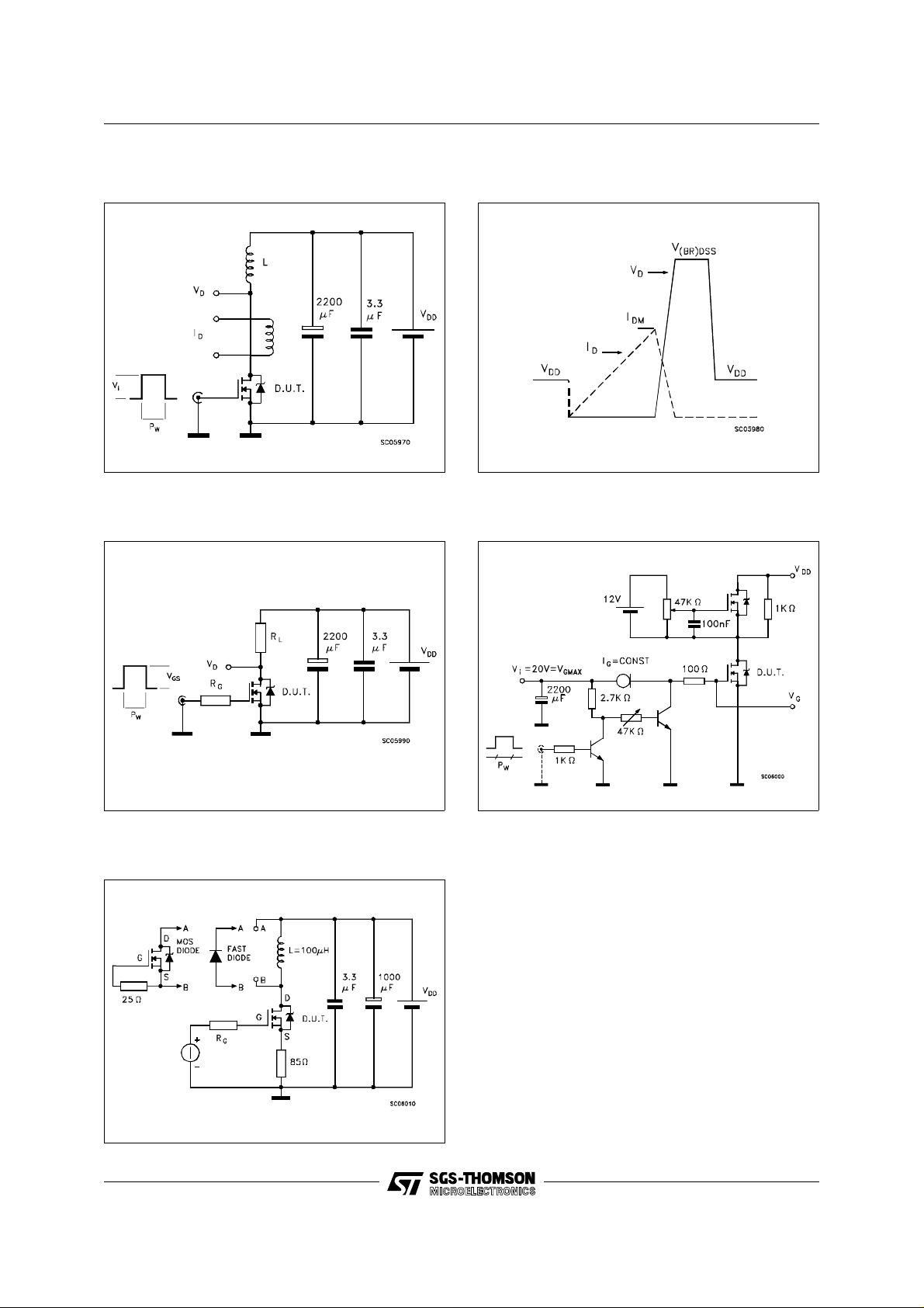
Fig. 1: Unclamped Inductive Load Test Circuits
Fig. 3: Switching Times Test Circuits For
Resistive Load
Fig. 2: Unclamped Inductive Waveforms
Fig. 4: Gate Charge Test Circuit
Fig. 5: Test Circuit For Inductive Load Switching
And Diode Reverse Recovery Time
4/7
E
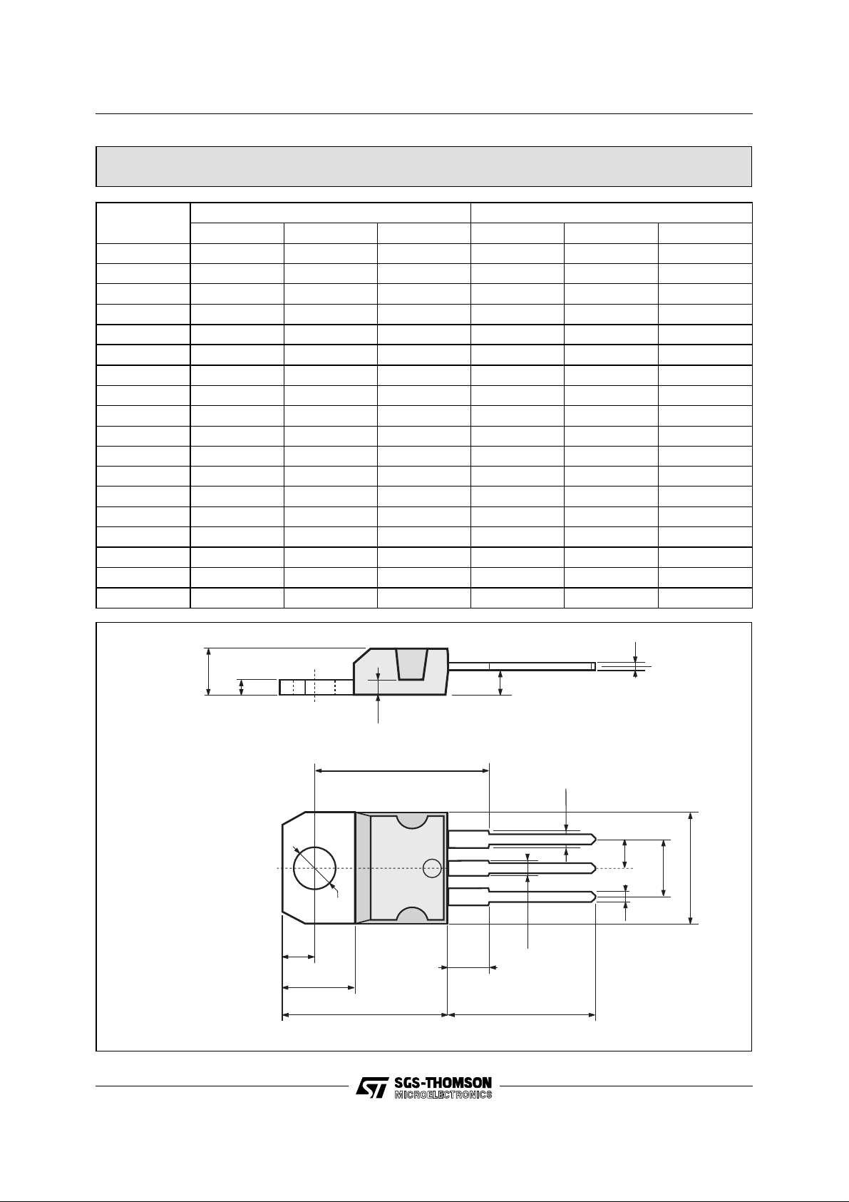
TO-220 MECHANICAL DATA
STP19N06L/FI
DIM.
MIN. TYP. MAX. MIN. TYP. MAX.
A 4.40 4.60 0.173 0.181
C 1.23 1.32 0.048 0.051
D 2.40 2.72 0.094 0.107
D1 1.27 0.050
E 0.49 0.70 0.019 0.027
F 0.61 0.88 0.024 0.034
F1 1.14 1.70 0.044 0.067
F2 1.14 1.70 0.044 0.067
G 4.95 5.15 0.194 0.203
G1 2.4 2.7 0.094 0.106
H2 10.0 10.40 0.393 0.409
L2 16.4 0.645
L4 13.0 14.0 0.511 0.551
L5 2.65 2.95 0.104 0.116
L6 15.25 15.75 0.600 0.620
L7 6.2 6.6 0.244 0.260
L9 3.5 3.93 0.137 0.154
DIA. 3.75 3.85 0.147 0.151
mm inch
A
C
D
D1
L2
F1
L5
Dia.
G1
F
F2
L9
G
H2
L7
L6
L4
P011C
5/7

STP19N06L/FI
ISOWATT220 MECHANICAL DATA
DIM.
MIN. TYP. MAX. MIN. TYP. MAX.
A 4.4 4.6 0.173 0.181
B 2.5 2.7 0.098 0.106
D 2.5 2.75 0.098 0.108
E 0.4 0.7 0.015 0.027
F 0.75 1 0.030 0.039
F1 1.15 1.7 0.045 0.067
F2 1.15 1.7 0.045 0.067
G 4.95 5.2 0.195 0.204
G1 2.4 2.7 0.094 0.106
H 10 10.4 0.393 0.409
L2 16 0.630
L3 28.6 30.6 1.126 1.204
L4 9.8 10.6 0.385 0.417
L6 15.9 16.4 0.626 0.645
L7 9 9.3 0.354 0.366
Ø 3 3.2 0.118 0.126
mm inch
A
B
H
Ø
L6
L7
L2
L3
D
F1
F2
F
123
L4
E
G1
G
P011G
6/7

STP19N06L/FI
Information furnished is believed to be accurate and reliable. However, SGS-THOMSON Microelectronics assumes no responsability for the
consequences of use of such information nor for any infringement of patents or other rights of third parties which may results from its use. No
license is granted by implication or otherwise under any patent or patent rights of SGS-THOMSON Microelectronics. Specifications mentioned
in this publication are subject to change without notice. This publication supersedes and replaces all information previously supplied.
SGS-THOMSON Microelectronics products are not authorized for use as critical components in life support devices or systems without express
written approval of SGS-THOMSON Microelectonics.
© 1994 SGS-THOMSON Microelectronics - All Rights Reserved
Australia - Brazil - France - Germany - Hong Kong - Italy - Japan - Korea - Malaysia - Malta - Morocco - The Netherlands -
Singapore - Spain - Sweden - Switzerland - Taiwan - Thailand - United Kingdom - U.S.A
SGS-THOMSON Microelectronics GROUP OF COMPANIES
7/7
 Loading...