

ST STP16NS25, STP16NS25FP User Manual
查询STP16NS25供应商
N-CHANNEL 250V - 0.23Ω - 16A TO-220 / TO-220FP
STP16N S25
STP16NS25FP
MESH OVERLAY™ MOSFET
TYPE V
STP16NS25
STP16NS25 FP
■ TYPICAL R
■ EXTREMELY HIGH dv /d t CAPABILITY
■ 100% AVALANCHE TESTED
DS
DSS
250 V
250 V
(on) = 0.23 Ω
R
DS(on)
< 0.28 Ω
< 0.28 Ω
I
D
16 A
16 A
DESCRIPTION
Using the latest high voltage MESH OVERLAY™
process, STMicroelectronics has designed an advanced family of power MOSFETs with outstanding
performance. The new patented STrip layout coupled with the Company’s proprietary edge termination structure, makes it suitable in coverters for
lighting applications.
APPLICATIONS
■ HIGH CURRENT, HIGH SPEED SWITCHING
■ SWITH MODE POWER SUPPLI ES (SMPS)
■ DC-DC CONVERTERS FOR TELECOM,
INDUSTRIAL, AND LIGHTING EQUIPMENT
■ IDEAL FOR MONITOR’s B+ FUNCTION
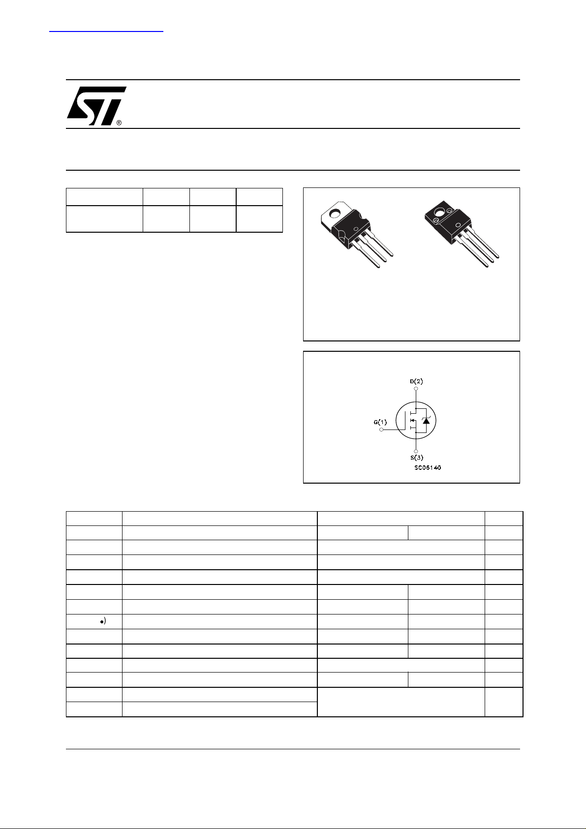
3
2
1
TO-220
TO-220FP
INTERNAL SCHEMATIC DIAGRAM
3
2
1
ABSOLUTE MAXIMUM RATINGS
Symbol Parameter Value Unit
STP16NS25 STP16NS25FP
V
DS
V
DGR
V
GS
I
D
I
D
I
DM
P
TOT
dv/dt (1) Peak Diode Recovery voltage slope 5 V/ns
V
ISO
T
stg
T
j
(•)Pu l se width limite d by safe operat i ng area
Drain-source Voltage (VGS = 0)
Drain-gate Voltage (RGS = 20 kΩ)
250 V
250 V
Gate- source Voltage ± 20 V
Drain Current (continuos) at TC = 25°C
Drain Current (continuos) at TC = 100°C
(l)
Drain Current (pulsed) 64 64(*) A
Total Dissipation at TC = 25°C
16 16(*) A
11 11(*) A
140 40 W
Derating Factor 1 0.33 W/°C
Insulation Withstand Voltage (DC) - 2500 V
Storage Temperature
Max. Operating Junction Temperature
(1) ISD≤ 16A, di/dt≤300 A/µs, VDD≤ V
(*) Limite d only by maximum temperat ure allowed
–65 to 150 °C
, Tj≤T
(BR)DSS
jMAX
1/9May 2002
STP16NS25 - STP16NS25FP
THERMA L D ATA
TO-220 TO-220FP °C/W
Rthj-case Thermal Resistance Junction-case Max 0.9 3 °C/W
Rthj-amb Thermal Resistance Junction-ambient Max 62.5 °C/W
T
l
AVALANCHE CHARACTERISTICS
Symbol Parameter Max Value Unit
I
AR
E
AS
ELECTRICAL CHARACTERISTICS (TCASE = 25 °C UNLESS OTHERWISE SPECIFIED)
OFF
Symbol Parameter Test Conditions Min. Typ. Max. Unit
V
(BR)DSS
I
DSS
I
GSS
Maximum Lead Temperature For Soldering Purpose 300 °C
Avalanche Current, Repetitive or Not-Repetitive
(pulse width limited by T
max)
j
Single Pulse Avalanche Energy
(starting T
Drain-source
= 25 °C, ID = IAR, VDD = 50 V)
j
ID = 250 µA, VGS = 0 250 V
16 A
600 mJ
Breakdown Voltage
= Max Rating
Zero Gate Voltage
Drain Current (V
GS
Gate-body Leakage
Current (V
DS
= 0)
= 0)
V
DS
V
= Max Rating, TC = 125 °C
DS
V
= ± 20 V ±100 nA
GS
1µA
10 µA
ON
(1)
Symbol Parameter Test Conditions Min. Typ. Max. Unit
V
V
GS(th)
R
DS(on)
Gate Threshold Voltage
Static Drain-source On
= VGS, ID = 250µA
DS
VGS = 10V, ID = 8 A
234V
0.23 0.28 Ω
Resistance
DYNAMIC
Symbol Parameter Test Conditions Min. Typ. Max. Unit
(1) Forward Transconductance VDS > I
g
fs
C
iss
C
oss
C
rss
Input Capacitance
Output Capacitance 190 pF
Reverse Transfer
Capacitance
ID=8 A
V
DS
D(on)
x R
DS(on)max,
= 25V, f = 1 MHz, VGS = 0
15 S
1270 pF
74 pF
2/9
STP16NS25 - STP16NS25FP
ELECTRICAL CHARACTERISTICS (CONTINUED)
SWITCHING ON
Symbol Parameter Test Conditions Min. Typ. Max. Unit
V
t
d(on)
Q
Q
Q
t
r
g
gs
gd
Turn-on Delay Time
Rise Time 26 ns
Total Gate Charge
Gate-Source Charge 7.9 nC
Gate-Drain Charge 22.3 nC
SWITCHING OFF
Symbol Parameter Test Conditions Min. Typ. Max. Unit
t
d(Voff)
t
r(Voff)
t
t
f
t
f
c
Turn-off- Delay Time
Fall Time
Off-voltage Rise Time
Fall Time
Cross-over Time
SOURCE DRAIN DIODE
Symbol Parameter Test Conditions Min. Typ. Max. Unit
I
SD
I
SDM
VSD (1)
t
rr
Q
rr
I
RRM
Note: 1. Pulsed: Pu l se duration = 300 µ s, duty cycle 1. 5 %.
2. Pulse width li mited by safe operating area.
Source-drain Current 16 A
(2)
Source-drain Current (pulsed) 64 A
Forward On Voltage
Reverse Recovery Time
Reverse Recovery Charge 1.5 µC
Reverse Recovery Current 11.4 A
= 125 V, ID = 8 A
DD
RG= 4.7Ω VGS = 10 V
(see test circuit, Figure 3)
V
= 200V, ID = 16 A,
DD
VGS = 10V
VDD = 125V, ID = 8 A,
RG=4.7Ω, V
GS
= 10V
(see test circuit, Figure 3)
V
= 200V, ID = 16 A,
clamp
R
=4.7Ω, V
G
GS
= 10V
(see test circuit, Figure 5)
ISD = 16 A, VGS = 0
I
= 16 A, di/dt = 100A/µs
SD
VDD = 30V, Tj = 150°C
(see test circuit, Figure 5)
14.5 ns
59 83 nC
72
32
24
28
56
1.5 V
270 ns
ns
ns
ns
ns
ns
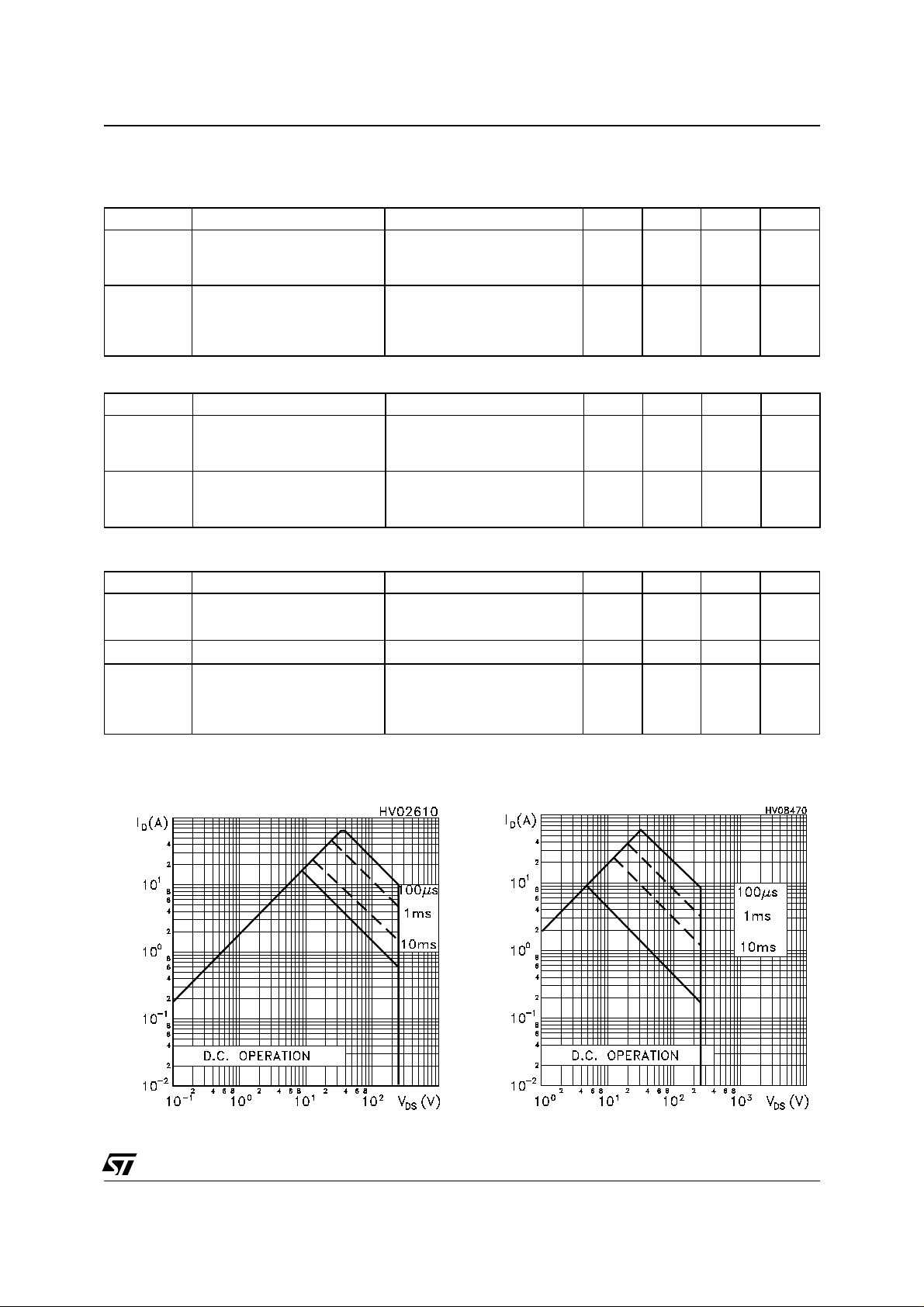
Safe Operating Area for TO-220FPSafe Operating Area for TO-220
3/9
 Loading...