

Features
■ Step-up and inverter converters
■ Operating input voltage range from 2.5 V to
4.5 V
■ Synchronous rectification for both DC-DC
converters
■ Minimum 200 mA output current
■ 4.6 V fixed positive output voltage
■ Programmable negative voltage by S
WIRE
from
-2.4 V to -5.4 V at 100 mV steps
■ Typical efficiency: 85%
■ Pulse skipping mode in light load condition
■ 1.5 MHz PWM mode control switching
frequency
■ Enable pin for shutdown mode
■ Low quiescent current in shutdown mode
■ Soft-start with inrush current protection
■ Overtemperature protection
■ Temperature range: -40 °C to 85 °C
■ True-shutdown mode
■ Fast discharge outputs of the circuits after
shutdown
■ Short-circuit protection
■ Package DFN12L (3 x 3 mm) 0.6 mm height
Applications
■ Active matrix AMOLED power supply
■ Cellular phones
■ Camcorders and digital still cameras
■ Multimedia players
STOD03AS
Dual DC-DC converter
for powering AMOLED displays
DFN12L (3 x 3 mm)
Description
The STOD03AS is a dual DC-DC converter with
short-circuit protection for AMOLED display
panels. It integrates a step-up and an inverting
DC-DC converter making it particularly suitable
for battery operated products, in which the major
concern is overall system efficiency. It works in
pulse skipping mode during light load conditions
and PWM-MODE at 1.5 MHz frequency for
medium/high load conditions. The high frequency
allows the value and size of external components
to be reduced. The Enable pin allows the device
to be turned off, therefore reducing the current
consumption to less than 1 µA. The negative
output voltage can be programmed by an MCU
through a dedicated pin which implements singlewire protocol. Soft-start with controlled inrush
current limit and thermal shutdown are integrated
functions of the device.
Table 1. Device summary
Order code Positive voltage Negative voltage Package Packaging
STOD03ASTPUR 4.6V -2.4V to -5.4V DFN12L (3 x 3 mm) 3000 parts per reel
December 2011 Doc ID 022614 Rev 1 1/24
www.st.com
24

Contents STOD03AS
Contents
1 Schematic . . . . . . . . . . . . . . . . . . . . . . . . . . . . . . . . . . . . . . . . . . . . . . . . . 3
2 Pin configuration . . . . . . . . . . . . . . . . . . . . . . . . . . . . . . . . . . . . . . . . . . . . 5
3 Maximum ratings . . . . . . . . . . . . . . . . . . . . . . . . . . . . . . . . . . . . . . . . . . . . 6
4 Electrical characteristics . . . . . . . . . . . . . . . . . . . . . . . . . . . . . . . . . . . . . 7
5 Typical performance characteristics . . . . . . . . . . . . . . . . . . . . . . . . . . . 10
6 Detailed description . . . . . . . . . . . . . . . . . . . . . . . . . . . . . . . . . . . . . . . . 12
6.1 S
6.1.1 S
6.1.2
6.1.3
. . . . . . . . . . . . . . . . . . . . . . . . . . . . . . . . . . . . . . . . . . . . . . . . . . . . 12
WIRE
features and benefits . . . . . . . . . . . . . . . . . . . . . . . . . . . . . . . . . 12
WIRE
S
S
protocol . . . . . . . . . . . . . . . . . . . . . . . . . . . . . . . . . . . . . . . . . . . 12
WIRE
basic operations . . . . . . . . . . . . . . . . . . . . . . . . . . . . . . . . . . . . . 12
WIRE
6.2 Negative output voltage levels . . . . . . . . . . . . . . . . . . . . . . . . . . . . . . . . . 12
7 Application information . . . . . . . . . . . . . . . . . . . . . . . . . . . . . . . . . . . . . 14
7.1 External passive components . . . . . . . . . . . . . . . . . . . . . . . . . . . . . . . . . 14
7.1.1 Inductor selection . . . . . . . . . . . . . . . . . . . . . . . . . . . . . . . . . . . . . . . . . . 14
7.1.2 Input and output capacitor selection . . . . . . . . . . . . . . . . . . . . . . . . . . . 14
7.2 Recommended PCB layout . . . . . . . . . . . . . . . . . . . . . . . . . . . . . . . . . . . 15
8 Detailed description . . . . . . . . . . . . . . . . . . . . . . . . . . . . . . . . . . . . . . . . 17
8.1 General description . . . . . . . . . . . . . . . . . . . . . . . . . . . . . . . . . . . . . . . . . 17
8.1.1 Multiple operation modes . . . . . . . . . . . . . . . . . . . . . . . . . . . . . . . . . . . . 17
8.1.2 Pulse skipping operation . . . . . . . . . . . . . . . . . . . . . . . . . . . . . . . . . . . . 17
8.1.3 Discontinuous conduction mode . . . . . . . . . . . . . . . . . . . . . . . . . . . . . . 17
8.1.4 Continuous conduction mode . . . . . . . . . . . . . . . . . . . . . . . . . . . . . . . . 17
8.1.5 Enable pin . . . . . . . . . . . . . . . . . . . . . . . . . . . . . . . . . . . . . . . . . . . . . . . 18
8.1.6 Soft-start and inrush current limiting . . . . . . . . . . . . . . . . . . . . . . . . . . . 18
8.1.7 Undervoltage lockout . . . . . . . . . . . . . . . . . . . . . . . . . . . . . . . . . . . . . . . 18
8.1.8 Overtemperature protection . . . . . . . . . . . . . . . . . . . . . . . . . . . . . . . . . . 18
8.1.9 Short-circuit protection . . . . . . . . . . . . . . . . . . . . . . . . . . . . . . . . . . . . . . 18
2/24 Doc ID 022614 Rev 1

STOD03AS Contents
8.1.10 Fast discharge . . . . . . . . . . . . . . . . . . . . . . . . . . . . . . . . . . . . . . . . . . . . 18
9 Package mechanical data . . . . . . . . . . . . . . . . . . . . . . . . . . . . . . . . . . . . 20
10 Revision history . . . . . . . . . . . . . . . . . . . . . . . . . . . . . . . . . . . . . . . . . . . 23
Doc ID 022614 Rev 1 3/24
Schematic STOD03AS
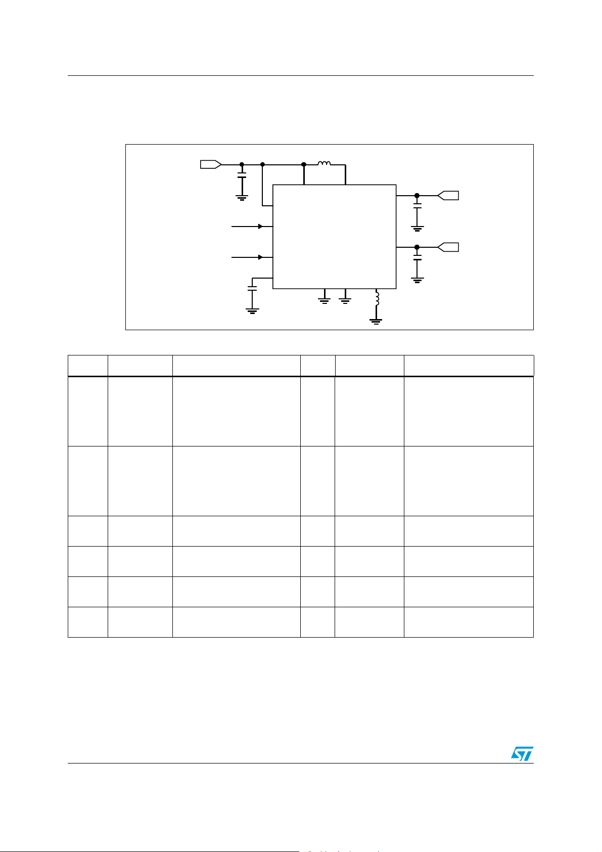
1 Schematic
Figure 1. Application schematic
6
"!4
#
).
6
).!
3
%.
6
7)2%
2%&
37IRE
%.
#
2%&
,
6
).0
34/$!3
0'.$ !'.$
,
8
6
-)$
#
-)$
6
/
#
/
,
8
,
!- V
Table 2. Typical external components
Comp. Manufacturer Part number Value Size Ratings
CoilCraft
Murata
(1)
L
1
SEMCO
ABCO
ABCO
CoilCraft
Murata
(2)
L
2
TOKO
ABCO
TDK
C
IN
C
MID
C
O2
C
REF
1. A 200 mA load can be provided with inductor saturation current as a minimum of 0.5 A.
2. At -5.4 V, a 200 mA load can be provided with inductor saturation current as a minimum of 1 A. See Section 7.1.1.
Murata
Taiyo Yuden
Murata
Taiyo Yuden
Murata
Taiyo Yuden
Murata
Taiyo Yuden
LPS4012-472ML
LQH3NPN4R7MJ0
CIG22B4R7MNE
LPF2810T-4R7M
LPF2807T-4R7M
LPS4012-472ML
LQH3NPN4R7MJ0
DFE252012C1239AS-H4R7N
LPF3510T-4R7M
VLF4014AT-4R7M1R1
GRM219R61A106KE44
LMK212BJ106KD-T
GRM219R61A106KE44
LMK212BJ106KD-T
GRM219R61A106KE44
LMK212BJ106KD-T
GRM185R60J105KE26
JMK107BJ105KK-T
4.7µH
4.7µH
2 x
10µF
10µF
2 x
10µF
1µF
4.0 x 4.0 x 1.2
3.0 x 3.0 x 1.1
2.5 x 2.0 x 1.0
2.8 x 2.8 x 1.0
2.8 x 2.8 x 0.7
4.0 x 4.0 x 1.2
3.0 x 3.0 x 1.1
2.5 x 2.0 x 1.2
3.5 x 3.5 x 1.0
3.7 x 3.5 x 1.4
0805
0805
0805
0805
0805
0805
0603
0603
±20%, I = 1.7 A, R = 0.175Ω
±20%, I = 1.1 A, R = 0.156Ω
±20%, I = 1.1 A, R = 0.300Ω
±20%, I = 0.85 A, R = 0.33Ω
±20%, I = 0.70 A, R = 0.44Ω
±20%, I = 1.7 A, R = 0.175Ω
±20%, I = 1.1 A, R = 0.156Ω
±30%, I = 1.2 A, R = 0.252Ω
±20%, I = 0.83 A, R = 0.25Ω
±20%, I = 1.1 A, R = 0.140Ω
±10%, X5R, 10V
±10%, X5R, 10V
±10%, X5R, 10V
±10%, X5R, 10V
±10%, X5R, 10V
±10%, X5R, 10V
±10%, X5R, 6.3V
±10%, X5R, 6.3V
Note: All the above components refer to the typical application performance characteristics.
Operation of the device is not limited to the choice of these external components. Inductor
values ranging from 3.3 µH to 6.8 µH can be used together with the STOD03AS.
4/24 Doc ID 022614 Rev 1
STOD03AS Schematic
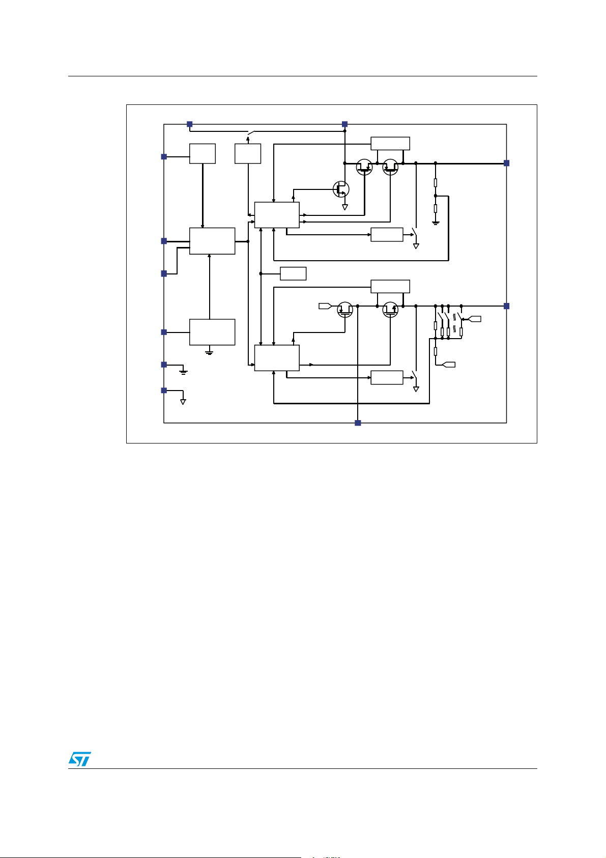
Figure 2. Block schematic
6
).0
,
8
6
).!
%.
3
7)2%
6
2%&
!'.$
0'.$
56,/
,/')##/.42/,
/40
37)2%
62%&
2).'
+),,%2
34%050
#/.42/,
).6%24).'
#/.42/,
/3#
6).0
$-$
6
-)$
0!
0"
.
&!3 4
$)3#(!2'%
$-$
6
0
.
3WIRE
CONTROL
62%&
&!3 4
$)3#(!2'%
,
8
/
!-V
Doc ID 022614 Rev 1 5/24

Pin configuration STOD03AS
2 Pin configuration
Figure 3. Pin configuration (top view)
Table 3. Pin description
Pin name Pin n° Description
Lx
1
1 Switching node of the step-up converter
PGND 2 Power ground pin
V
MID
3 Step-up converter output voltage (4.6V)
NC 4 Not internally connected
AGND 5 Signal ground pin. This pin must be connected to the power ground pin
Voltage reference output. 1µF bypass capacitor must be connected
V
REF
S
WIRE
EN 8
V
O2
Lx
2
V
IN A
V
iN P
6
between this pin and AGND
7 Negative voltage setting pin
Enable control pin. ON = V
. When pulled low it puts the device in
INA
shutdown mode
9 Inverting converter output voltage (Default - 4.9V)
10 Switching node of the inverting converter
11 Analogic input supply voltage
12 Power input supply voltage
Exposed
pad
Internally connected to AGND. Exposed pad must be connected to AGND
and PGND in the PCB layout in order to guarantee proper operation of the
device
6/24 Doc ID 022614 Rev 1

STOD03AS Maximum ratings
3 Maximum ratings
Table 4. Absolute maximum ratings
Symbol Parameter Value Unit
V
INA
EN, S
IL
L
V
V
L
IL
V
P
T
, V
X2
X2
O2
MID
X1
X1
REF
D
STG
T
J
WIRE
DC supply voltage -0.3 to 6 V
INP
Logic input pins -0.3 to 4.6 V
Inverting converter switching current Internally limited A
Inverting converter switching node voltage - 10 to V
+ 0.3 V
INP
Inverting converter output voltage - 10 to AGND + 0.3 V
Step-up converter and LDO output voltage -0.3 to 6 V
Step-up converter switching node voltage -0.3 to V
+ 0.3 V
MID
Step-up converter switching current Internally limited A
Reference voltage -0.3 to 3 V
Power dissipation Internally limited mW
Storage temperature range -65 to 150 °C
Maximum junction temperature 150 °C
ESD ESD protection HBM 2 kV
Note: Absolute maximum ratings are those values beyond which damage to the device may occur.
Functional operation under these conditions is not implied.
Table 5. Thermal data
Symbol Parameter Value Unit
R
thJA
R
thJC
1. The package is mounted on a 4-layer (2S2P) JEDEC board as per JESD51-7.
Thermal resistance junction-ambient 33 °C/W
Thermal resistance junction-case (FR-4 PCB)
(1)
2.12 °C/W
Doc ID 022614 Rev 1 7/24
Electrical characteristics STOD03AS
4 Electrical characteristics
TJ = 25 °C, V
C
= 2 x 10 µF, C
O2
INA
= V
= 3.7 V, I
INP
= 1 µF, L1 = L2 = 4.7 µH, V
REF
MID,O2
= 30 mA, C
= 2 x 10 µF, C
IN
= 2 V, V
EN
= 10 µF,
MID
= 4.6 V, VO2= -4.9 V unless
MID
otherwise specified.
Table 6. Electrical characteristics
Symbol Parameter Test conditions Min. Typ. Max. Unit
General section
V
INA, VINP
UVLO_H Undervoltage lockout HIGH V
UVLO_L Undervoltage lockout LOW V
I_V
I
Q_SH
V
EN
V
EN
I
EN
f
D1
D2
η Total system efficiency
V
REF
I
REF
Supply input voltage 2.3 3.7 4.5 V
rising 2.22 2.25 V
INA
falling 1.9 2.18 V
INA
Input current No load condition 1.7 2.1 mA
I
=GND
V
Shutdown current
H Enable high threshold
L Enable low threshold 0.4
Enable input current
S
MAX
MAX
Switching frequency PWM mode 1.2 1.5 1.7 MHz
Step-up maximum duty cycle No load 87 %
Inverting maximum duty cycle No load 87 %
Voltage reference I
Voltage reference current
capability
EN
TJ=-40°C to +85°C
V
=2.5V to 4.5V,
INA
1.2
TJ=-40°C to +85°C
V
EN=VINA
=-40°C to +85°C
T
J
I
MID,O2
V
MID
I
MID,O2
V
MID
REF
At 98.5% of no load
reference voltage
=4.5V
=10 to 30mA,
=4.6V, VO2=-4.9V
=30 to 150mA,
=4.6V, VO2=-4.9V
80 %
85 %
=10µA 1.216 1.228 1.240 V
100 µA
1µA
1µA
V
Step-up converter section
Positive voltage total variation
V
INA=VINP
I
MID
=2.5V to 4.5V;
=5mA to 150mA, IO2 no
load, TJ=25°C
V
MID
Temperature accuracy
V
INA=VINP
I
O2
=3.7V; I
no load; TJ=-40°C to
MID
+85°C
=3.5V to 3.0V,
V
ΔV
MID LT
Line transient
INA,P
=100mA; TR=TF=50µs
I
MID
8/24 Doc ID 022614 Rev 1
4.55 4.6 4.65 V
=5mA;
±0.5 %
-12 mV
 Loading...