

查询STF817供应商
STF817
®
PNP MEDIUM POWER TRANSISTORS
Type Marking
STF817 817
STN817 N817
■ SURFACE-MOUNTING DEVICES IN
MEDIUM POWE R SO T-223 AND SO T-89
PACKAGES
■ AVAILABLE IN TAPE & REEL PACKING
APPLICATIONS
■ VOLTAGE REGULATION
■ RELAY DRIVER
■ GENERIC SWITCH
DECRIPTION
The STF817 and STN817 are PNP transistors
manufactured using Planar Technology resulting
in rugged high performance devices.
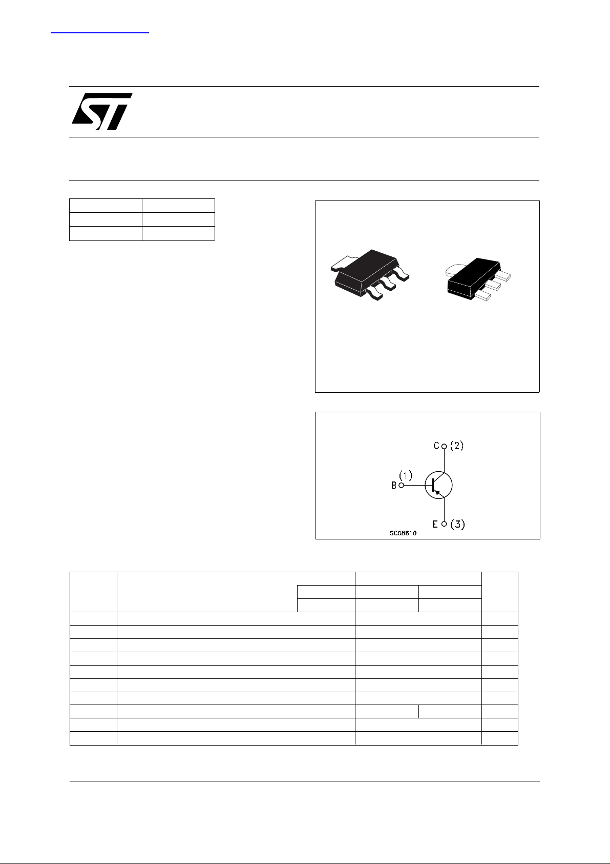
2
1
SOT-223
STN817
3
2
SOT-89
INTERNAL SCHEMATIC DIAGRAM
ABSOL UT E MAXIMU M RATINGS
Symbol Parameter Value Unit
Devices STN817 STF817
Packages SOT-223 SOT-89
V
V
V
I
I
P
T
Collector-Base Voltage (IE = 0) -120 V
CBO
Collector-Emitter Voltage (IB = 0) -80 V
CEO
Emitter-Base Voltage (IC = 0) -5 V
EBO
I
Collector Current -1.5 A
C
Collector Peak Current (tp < 5 ms) -2 A
CM
I
Base Current -0.3 A
B
Base Peak Current (tp < 5 ms) -0.6 A
BM
Total Dissipation at Tc = 25 oC 1.6 1.4 W
tot
Storage Temperature -65 to 150
stg
T
Max. Operating Junction Temperature 150
j
o
C
o
C
April 2002
1/5
STF817 - STN817
THERMAL DATA
R
• Device mounted on a PCB area of 1 cm2.
• Thermal Resistance Junction-ambient Max 78 89
thj-amb
SOT-223 SOT-89
o
C/W
ELECTRICAL CHARACTERISTICS (T
= 25 oC unless otherwise specified)
case
Symbol Parameter Test Conditions Min. Typ. Max. Unit
I
CES
I
CEO
I
EBO
V
CEO(sus)
Collector Cut-off
Current (V
BE
= 0)
Collector Cut-off
Current (I
= 0)
B
Emitter Cut-off Current
(I
= 0)
C
∗ Collector-Emitter
= -120 V -500 µA
V
CE
= -80 V -1 mA
V
CE
= -5 V -100 µA
V
EB
I
= -10 mA -80 V
C
Sustaining Voltage
(I
= 0)
B
V
V
∗ Pulsed: Pulse duration = 300 µs, duty cycle 1.5 %
∗ Collector-Emitter
CE(sat)
Saturation Voltage
∗ Base-Emitter
BE(sat)
Saturation Voltage
h
∗ DC Current Gain IC = -100 mA VCE = -2 V
FE
f
Transition Frequency IC = -0.1 A VCE = -10 V 50 MHz
T
IC = -100 mA IB = -10 mA
I
= -1 A IB = -100 mA
C
IC = -100 mA IB = -10 mA
I
= -1 A IB = -100 mA
C
I
= -500 mA VCE = -2 V
C
I
= -1 A VCE = -2 V
C
-0.25
-0.5
-1
-1.1
140
80
40
V
V
V
V
2/5
 Loading...