

ST STMUX1800L User Manual
Features
STMUX1800L
16- to 8-bit MUX/DEMUX for gigabit Ethernet LAN switch
with LED switch and enhanced ESD protection
■ Low R
■ V
CC
■ Enhanced ESD protection: > 8 kV (contact) and
: 4.0 Ω typical
ON
operating range: 3.0 to 3.6 V
15 kV (HBM)
■ Channel on capacitance: 9.5 pF typical
■ Switching time speed: 9 ns
■ Near to zero propagation delay: 250 ps
■ Very low crosstalk: -45 dB at 250 MHz
■ Bit-to-bit skew: 200 ps
■ > 600 MHz -3 dB typical bandwidth (or data
frequency)
■ Three SPDT switches for LED support
■ Rail-to-rail switching on data I/O ports
(0 V to 5 V)
■ Package: QFN56
■ Pb-free
Applications
■ 10/100/1000 Mbit Ethernet switching
■ Audio/video switching
QFN56
Description
The STMUX1800L is a 16- to 8-bit
multiplexer/demultiplexer low R
LAN switch designed for various standards, such
as 10/100/1000 Ethernet. It is designed for very
low crosstalk, low bit-to-bit skew and low I/O
capacitance.
bidirectional
ON
The differential signal from the Gigabit Ethernet
transceiver is multiplexed into one of two selected
outputs while the unselected switch goes to Hi-Z
status.
The device integrates three SPDT (single pole
dual throw) switches, for LED support.
Table 1. Device summary
Order code Package Packing
STMUX1800LQTR QFN56 Tape and reel
June 2009 Doc ID 14869 Rev 4 1/21
www.st.com
21

Contents STMUX1800L
Contents
1 Pin description . . . . . . . . . . . . . . . . . . . . . . . . . . . . . . . . . . . . . . . . . . . . . 3
2 Maximum ratings . . . . . . . . . . . . . . . . . . . . . . . . . . . . . . . . . . . . . . . . . . . . 6
2.1 Recommended operating conditions . . . . . . . . . . . . . . . . . . . . . . . . . . . . . 6
3 Electrical characteristics . . . . . . . . . . . . . . . . . . . . . . . . . . . . . . . . . . . . . 7
4 Package mechanical data . . . . . . . . . . . . . . . . . . . . . . . . . . . . . . . . . . . . 16
5 Revision history . . . . . . . . . . . . . . . . . . . . . . . . . . . . . . . . . . . . . . . . . . . 20
2/21 Doc ID 14869 Rev 4
STMUX1800L Pin description
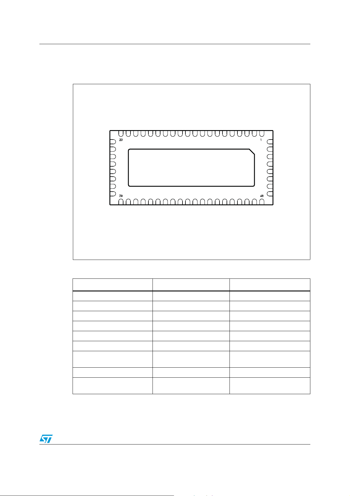
1 Pin description
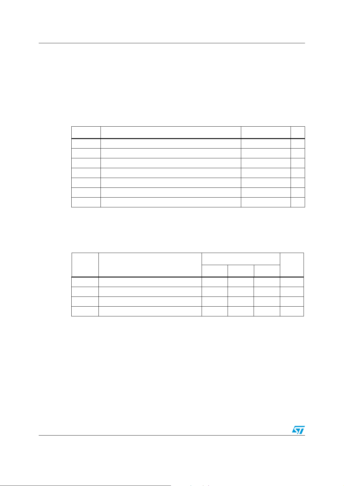
Figure 1. Pin connection (top through view)
LED2
LED1
VDD
SEL
GNDHG
GNDFE
VDD
GNDDC
GND
N/C
VDDBA
GND
GND
LED1_0
LED2_0
GND
LED1_1
LED2_1
VDD
GND
F1
F0
H1G1H0
G0
GND
E1
E0
VDD
D1C1D0
GND
C0
GND
B1A1B0
A0
Table 2. Pin description
Pin Symbol Name and function
2, 3, 7, 8, 11, 12, 14, 15 A, B, C, D, E, F, G, H 8-bit bus
48, 47, 43, 42, 37, 36, 32, 31 A0, B0, C0, D0, E0, F0, G0, H0 8-bit multiplexed to bus 0
46, 45, 41, 40, 35, 34, 30, 29 A1, B1, C1, D1, E1, F1, G1, H1 8-bit multiplexed to bus 1
VDD
GND
LED3
GND
LED3_0
LED3_1
VDD
GND
CS000103
5 N/C Not connected
17 SEL Bus and LED switch selection
19, 20, 54 LED1, LED2, LED3 LED switch input
22, 23, 25, 26, 51, 52
4, 10, 18, 27, 38, 50, 56 V
1, 6, 9, 13, 16, 21, 24, 28, 33,
39, 44, 49, 53, 55
LED1_0, LED2_0, LED1_1,
LED2_1, LED3_1, LED3_0
DD
GND Ground
LED switch output
Supply voltage
Doc ID 14869 Rev 4 3/21
Pin description STMUX1800L
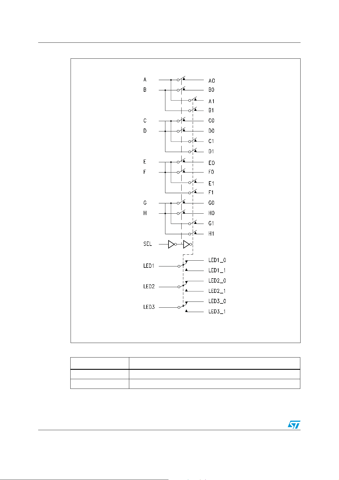
Figure 2. Input equivalent circuit
Table 3. LAN switch function table
SEL Function
L 8-bit bus to 8-bit multiplexed bus 0
H 8-bit bus to 8-bit multiplexed bus 1
4/21 Doc ID 14869 Rev 4
CS000104
STMUX1800L Pin description
Table 4. LED switch function table
SEL Function
L LED switch input connected to LED switch output X_0
H LED switch input connected to LED switch output X_1
Doc ID 14869 Rev 4 5/21
Maximum ratings STMUX1800L
2 Maximum ratings
Stressing the device above the rating listed in the “absolute maximum ratings” table may
cause permanent damage to the device. These are stress ratings only and operation of the
device at these or any other conditions above those indicated in the operating sections of
this specification is not implied. Exposure to absolute maximum rating conditions for
extended periods may affect device reliability.
Table 5. Absolute maximum ratings
Symbol Parameter Value Unit
V
CC
V
V
I
O
P
T
stg
T
Supply voltage to ground -0.5 to 4.6 V
DC input output voltage -0.5 to 4.6 V
IO
DC control input voltage -0.5 to 4.6 V
IC
DC output current
Power dissipation 0.5 W
D
(1)
Storage temperature -65 to 150 °C
Lead temperature (10 sec) 300 °C
L
1. If VIO x IO does not exceed the maximum limit of PD.
2.1 Recommended operating conditions
Table 6. Recommended operating conditions
Symbol Parameter
V
V
V
T
Supply voltage to ground 3 – 3.6 V
CC
DC control input voltage (SEL) 0 – 5 V
IC
DC input/output voltage 0 – V
IO
Operating temperature -40 – 85 ° C
A
120 mA
Val ue
Min Typ Max
CC
Unit
V
6/21 Doc ID 14869 Rev 4
STMUX1800L Electrical characteristics
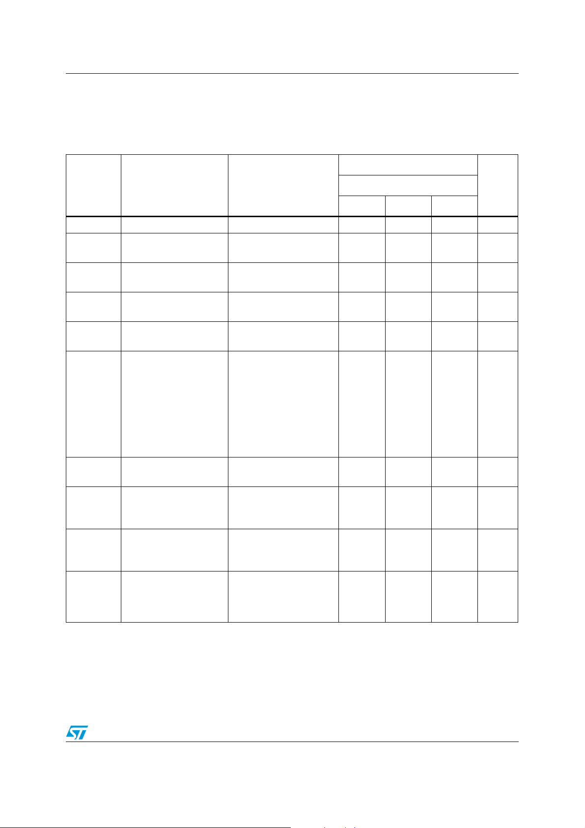
3 Electrical characteristics
Table 7. DC electrical characteristics for Gigabit Ethernet LAN8/16MUX/DEMUX
(V
= 3.3 V ±10%)
CC
Val ue
Symbol Parameter Test condition
Min Typ Max
IOFF
V
V
V
I
I
IH
IL
IK
IH
IL
(SW)
Voltage input high (SEL) High level guaranteed 2 – – V
Voltage input low
(SEL)
Clamp diode voltage
(SEL)
Input high current
(SEL)
Input low current
(SEL)
Leakage current through
the switch common
(1)
terminals (A to H)
(LED1 to LED3)
Low level guaranteed -0.5 – 0.8 V
VCC = 3.6 V
IIN = -18 mA
VCC = 3.6 V
= V
V
IN
CC
VCC = 3.6 V
= GND
V
IN
= 3.6 V
V
CC
A to H = V
CC
LED1 to LED3 = V
A0 to H0 = 0 V
A1 to H1 = floating
CC
– -0.8 -1.2 V
––±5µA
––±5µA
––±1µA
LEDx_0 = 0 V
LEDx1 = floating
IOFF
(SEL)
SEL pin leakage current
SEL = V
VCC= 0 V
SEL = 0 to 3.6 V
CC
––±1µA
VCC = 3.0 V
R
ON
Switch ON resistance
(2)
= 1.5 to V
V
IN
CC
–4.06.5Ω
IIN = -40 mA
Unit-40 to 85 °C
VCC = 3.0 V
R
FLAT
ON resistance flatness
(3)
ON resistance match
ΔR
1. Refer to Figure 4: Test circuit for leakage current (IOFF) on page 11
2. Measured by voltage drop between channels at indicated current through the switch. ON resistance is determined by the
lower of the voltages.
3. Flatness is defined as the difference between the R
ΔR
4.
ON
between channel
ON
ΔR
= R
ON
(2)(4)
measured at same VCC, temperature and voltage level.
ONMAX-RONMIN
(2)
V
IN
I
IN
VCC = 3.0 V
V
IN
IIN = -40 mA
at 1.5 and VCC
= -40 mA
= 1.5 to V
ONMAX
CC
and R
–0.5–Ω
–0.41Ω
of ON resistance over the specified range.
ONMIN
Doc ID 14869 Rev 4 7/21
 Loading...