

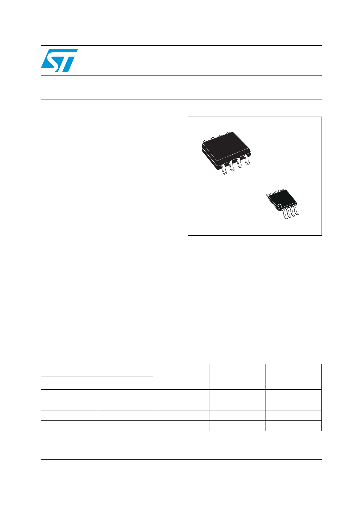
Enhanced dual-channel power switches
Features
■ 100 mΩ high-side MOSFET switch
■ 500 mA/1000 mA continuous current per
channel
■ Thermal protection
■ Independent short-circuit protection with
overcurrent logic output
■ Operating range from 2.7 V to 5.5 V
■ CMOS and TTL compatible inputs
■ 2.5 ms typical rise time
■ Undervoltage lockout
■ 13 µA maximum standby supply current
■ Ambient temperature range: -40 °C to 85 °C
■ 8 kV ESD protection
■ Reverse current protection
■ Fault blanking
Description
The STMPS2242/2252/2262/2272 power
distribution switches are intended for applications
where heavy capacitive loads and short-circuits
are likely to be encountered. These devices
incorporate 100 m
switches for power distribution systems that
require multiple power switches in a single
package.
Table 1. Device summary
Ω MOSFET high-side power
STMPS2242, STMPS2252
STMPS2262, STMPS2272
SO-8
MSOP8
Each switch is controlled by an independent logic
enable input. When the output load exceeds the
current limit threshold or a short is present, these
devices limit the output current to a safe level by
switching into a constant current mode, pulling the
overcurrent (OCx) logic output low. When
continuous heavy overloads and short-circuits
increase the power dissipation in the switch,
causing the junction temperature to rise, a
thermal protection circuit shuts off the switch to
prevent damage. Recovery from a thermal
shutdown is automatic once the device has
cooled sufficiently. Internal circuitry ensures the
switch remains off until valid input voltage is
present.
Order code
SO-8 MSOP8
STMPS2242MTR STMPS2242TTR 500 Active low Tape and reel
STMPS2252MTR STMPS2252TTR 500 Active high Tape and reel
STMPS2262MTR STMPS2262TTR 1000 Active low Tape and reel
STMPS2272MTR STMPS2272TTR 1000 Active high Tape and reel
1. MSOP8 is also known as TSSOP8.
January 2011 Doc ID 15050 Rev 3 1/42
(1)
Current limit
(mA)
Enable Packing
www.st.com
42

Contents STMPS2242, STMPS2252, STMPS2262, STMPS2272
Contents
1 Block diagram . . . . . . . . . . . . . . . . . . . . . . . . . . . . . . . . . . . . . . . . . . . . . . 6
2 Pin descriptions . . . . . . . . . . . . . . . . . . . . . . . . . . . . . . . . . . . . . . . . . . . . 7
3 Functional description . . . . . . . . . . . . . . . . . . . . . . . . . . . . . . . . . . . . . . . 8
3.1 Fault blanking . . . . . . . . . . . . . . . . . . . . . . . . . . . . . . . . . . . . . . . . . . . . . . . 8
3.2 Overcurrent/overtemperature protection . . . . . . . . . . . . . . . . . . . . . . . . . . 8
3.3 Reverse current blocking . . . . . . . . . . . . . . . . . . . . . . . . . . . . . . . . . . . . . . 8
3.4 UVLO . . . . . . . . . . . . . . . . . . . . . . . . . . . . . . . . . . . . . . . . . . . . . . . . . . . . . 8
4 Maximum rating . . . . . . . . . . . . . . . . . . . . . . . . . . . . . . . . . . . . . . . . . . . . . 9
4.1 Absolute maximum rating . . . . . . . . . . . . . . . . . . . . . . . . . . . . . . . . . . . . . . 9
4.2 Recommended operating conditions . . . . . . . . . . . . . . . . . . . . . . . . . . . . . 9
5 Electrical specifications . . . . . . . . . . . . . . . . . . . . . . . . . . . . . . . . . . . . . 10
6 Typical operating characteristics . . . . . . . . . . . . . . . . . . . . . . . . . . . . . 13
6.1 STMPS2242, STMPS2252 characteristics . . . . . . . . . . . . . . . . . . . . . . . . 13
6.1.1 Turn-on/off characteristics for VI = 3 V, R
6.1.2 Turn-on/off characteristics for V
6.1.3 UVLO characteristics . . . . . . . . . . . . . . . . . . . . . . . . . . . . . . . . . . . . . . . 20
6.1.4 Overcurrent protection characteristics . . . . . . . . . . . . . . . . . . . . . . . . . . 21
6.1.5 Other electrical characteristics . . . . . . . . . . . . . . . . . . . . . . . . . . . . . . . . 22
= 5 V, R
I
= 6 Ω . . . . . . . . . . . . . . . 13
LOAD
= 10 Ω . . . . . . . . . . . . . . 16
LOAD
6.2 STMPS2262, STMPS2272 characteristics . . . . . . . . . . . . . . . . . . . . . . . . 24
6.2.1 Turn-on/off characteristics for VI = 3 V, R
6.2.2 Turn-on/off characteristics for V
6.2.3 UVLO characteristics . . . . . . . . . . . . . . . . . . . . . . . . . . . . . . . . . . . . . . . 30
6.2.4 Overcurrent protection characteristics . . . . . . . . . . . . . . . . . . . . . . . . . . 32
6.2.5 Other electrical characteristics . . . . . . . . . . . . . . . . . . . . . . . . . . . . . . . . 33
= 5 V, R
I
= 3 Ω . . . . . . . . . . . . . . . 24
LOAD
= 5 Ω . . . . . . . . . . . . . . . 27
LOAD
7 Application information . . . . . . . . . . . . . . . . . . . . . . . . . . . . . . . . . . . . . 35
7.1 Input and output capacitors . . . . . . . . . . . . . . . . . . . . . . . . . . . . . . . . . . . 35
8 Package mechanical data . . . . . . . . . . . . . . . . . . . . . . . . . . . . . . . . . . . . 36
2/42 Doc ID 15050 Rev 3

STMPS2242, STMPS2252, STMPS2262, STMPS2272 Contents
9 Revision history . . . . . . . . . . . . . . . . . . . . . . . . . . . . . . . . . . . . . . . . . . . 41
Doc ID 15050 Rev 3 3/42

List of tables STMPS2242, STMPS2252, STMPS2262, STMPS2272
List of tables
Table 1. Device summary . . . . . . . . . . . . . . . . . . . . . . . . . . . . . . . . . . . . . . . . . . . . . . . . . . . . . . . . . . 1
Table 2. Pin descriptions . . . . . . . . . . . . . . . . . . . . . . . . . . . . . . . . . . . . . . . . . . . . . . . . . . . . . . . . . . 7
Table 3. Absolute maximum ratings . . . . . . . . . . . . . . . . . . . . . . . . . . . . . . . . . . . . . . . . . . . . . . . . . . 9
Table 4. Recommended operating conditions . . . . . . . . . . . . . . . . . . . . . . . . . . . . . . . . . . . . . . . . . . 9
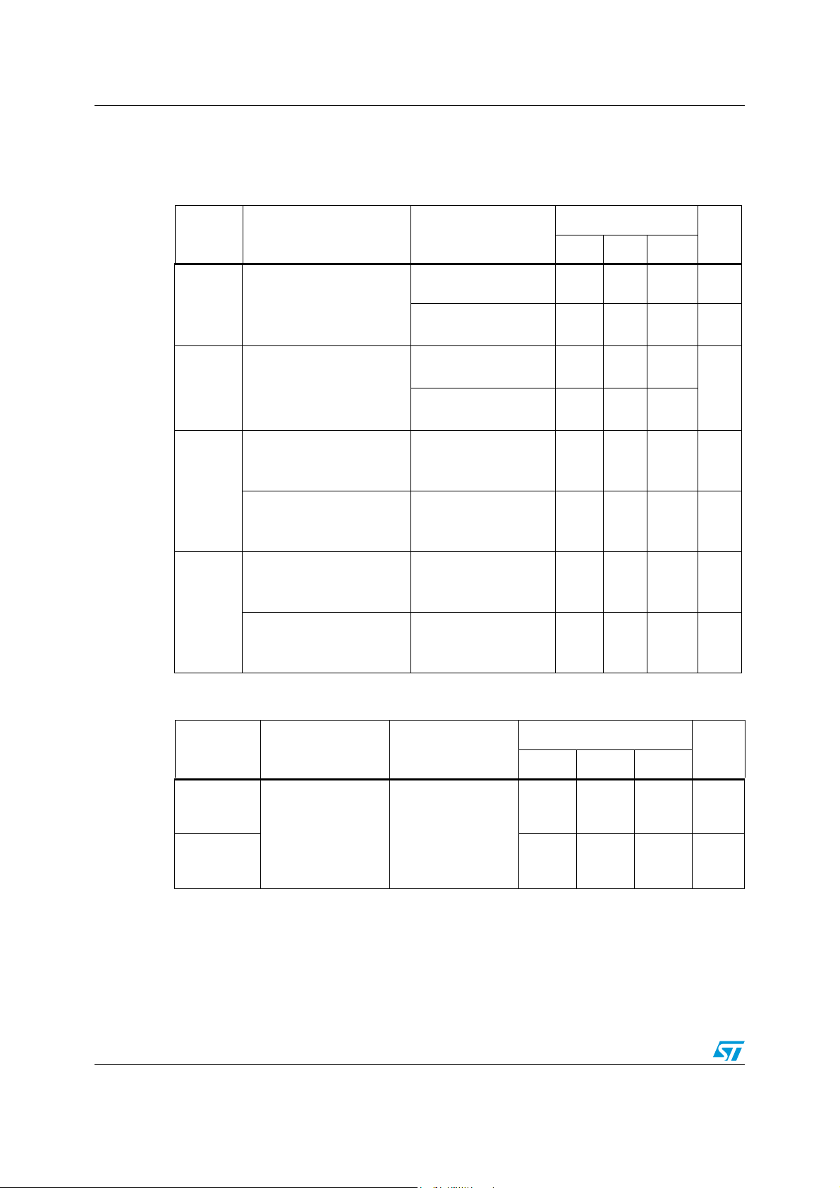
Table 5. Electrical characteristics . . . . . . . . . . . . . . . . . . . . . . . . . . . . . . . . . . . . . . . . . . . . . . . . . . . 10
Table 6. Current limit characteristics
(V
= 5.5 V, IO= rated current, TJ= 25°C, unless otherwise specified) . . . . . . . . . . . . . . . 10
Table 7. Supply current characteristics
Table 8. Thermal characteristics
Table 9. UVLO characteristics
Table 10. OCx pin characteristics
Table 11. ENx pin characteristics
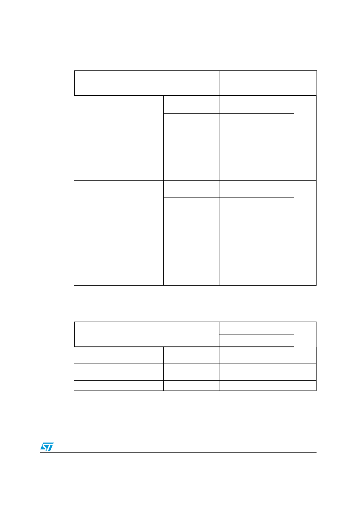
Table 12. SO-8 mechanical data . . . . . . . . . . . . . . . . . . . . . . . . . . . . . . . . . . . . . . . . . . . . . . . . . . . . 37
Table 13. MSOP8 mechanical data . . . . . . . . . . . . . . . . . . . . . . . . . . . . . . . . . . . . . . . . . . . . . . . . . . 38
Table 14. Reel mechanical data . . . . . . . . . . . . . . . . . . . . . . . . . . . . . . . . . . . . . . . . . . . . . . . . . . . . . 40
Table 15. Document revision history . . . . . . . . . . . . . . . . . . . . . . . . . . . . . . . . . . . . . . . . . . . . . . . . . 41
I
(V
= 5.5 V, IO= rated current, TJ= 25°C, unless otherwise specified) . . . . . . . . . . . . . . . 11
I
(V
= 5.5 V, IO= rated current, TJ= 25°C, unless otherwise specified) . . . . . . . . . . . . . . . 11
I
(V
= 5.5 V, IO= rated current, TJ= 25°C, unless otherwise specified) . . . . . . . . . . . . . . . 12
I
(V
= 5.5 V, IO= rated current, TJ= 25°C, unless otherwise specified) . . . . . . . . . . . . . . . 12
I
(V
= 5.5 V, IO= rated current, TJ= 25°C, unless otherwise specified) . . . . . . . . . . . . . . . 12
I
4/42 Doc ID 15050 Rev 3

STMPS2242, STMPS2252, STMPS2262, STMPS2272 List of figures
List of figures
Figure 1. Block diagram . . . . . . . . . . . . . . . . . . . . . . . . . . . . . . . . . . . . . . . . . . . . . . . . . . . . . . . . . . . . 6
Figure 2. Pinout . . . . . . . . . . . . . . . . . . . . . . . . . . . . . . . . . . . . . . . . . . . . . . . . . . . . . . . . . . . . . . . . . . 7
Figure 3. Turn-on for C
Figure 4. Turn-on for C
Figure 5. Turn-on for C
Figure 6. Turn-off for C
Figure 7. Turn-off for C
Figure 8. Turn-off for C
Figure 9. Turn-on for C
Figure 10. Turn-on for C
Figure 11. Turn-on for C
Figure 12. Turn-off for C
Figure 13. Turn-off for C
Figure 14. Turn-off for C
Figure 15. UVLO, V
Figure 16. UVLO, V
rising . . . . . . . . . . . . . . . . . . . . . . . . . . . . . . . . . . . . . . . . . . . . . . . . . . . . . . . . . . 20
I
falling . . . . . . . . . . . . . . . . . . . . . . . . . . . . . . . . . . . . . . . . . . . . . . . . . . . . . . . . . 20
I
Figure 17. Overcurrent protection characteristics, V
Figure 18. Overcurrent protection characteristics, V
Figure 19. I
Figure 20. t
Figure 21. t
versus VI. . . . . . . . . . . . . . . . . . . . . . . . . . . . . . . . . . . . . . . . . . . . . . . . . . . . . . . . . . . . 22
CC
versus VI . . . . . . . . . . . . . . . . . . . . . . . . . . . . . . . . . . . . . . . . . . . . . . . . . . . . . . . . . . . . . 22
r
versus VI . . . . . . . . . . . . . . . . . . . . . . . . . . . . . . . . . . . . . . . . . . . . . . . . . . . . . . . . . . . . . 23
f
Figure 22. Rds(on) versus V
Figure 23. Turn-on for C
Figure 24. Turn-on for C
Figure 25. Turn-on for C
Figure 26. Turn-off for C
Figure 27. Turn-off for C
Figure 28. Turn-off for C
Figure 29. Turn-on for C
Figure 30. Turn-on for C
Figure 31. Turn-on for C
Figure 32. Turn-off for C
Figure 33. Turn-off for C
Figure 34. Turn-off for C
Figure 35. UVLO, V
Figure 36. UVLO, V
rising . . . . . . . . . . . . . . . . . . . . . . . . . . . . . . . . . . . . . . . . . . . . . . . . . . . . . . . . . . 30
I
falling . . . . . . . . . . . . . . . . . . . . . . . . . . . . . . . . . . . . . . . . . . . . . . . . . . . . . . . . . 31
I
Figure 37. Overcurrent protection characteristics, V
Figure 38. Overcurrent protection characteristics, V
Figure 39. I
Figure 40. t
Figure 41. t
versus VI. . . . . . . . . . . . . . . . . . . . . . . . . . . . . . . . . . . . . . . . . . . . . . . . . . . . . . . . . . . . 33
CC
versus VI . . . . . . . . . . . . . . . . . . . . . . . . . . . . . . . . . . . . . . . . . . . . . . . . . . . . . . . . . . . . . 33
r
versus VI . . . . . . . . . . . . . . . . . . . . . . . . . . . . . . . . . . . . . . . . . . . . . . . . . . . . . . . . . . . . . 34
f
Figure 42. Rds(on) versus V
Figure 43. SO-8 package outline . . . . . . . . . . . . . . . . . . . . . . . . . . . . . . . . . . . . . . . . . . . . . . . . . . . . . 36
Figure 44. MSOP8 package outline . . . . . . . . . . . . . . . . . . . . . . . . . . . . . . . . . . . . . . . . . . . . . . . . . . . 38
Figure 45. SO-8 carrier tape . . . . . . . . . . . . . . . . . . . . . . . . . . . . . . . . . . . . . . . . . . . . . . . . . . . . . . . . 39
Figure 46. MSOP8 carrier tape . . . . . . . . . . . . . . . . . . . . . . . . . . . . . . . . . . . . . . . . . . . . . . . . . . . . . . 39
Figure 47. Reel information . . . . . . . . . . . . . . . . . . . . . . . . . . . . . . . . . . . . . . . . . . . . . . . . . . . . . . . . . 40
= 1 µF . . . . . . . . . . . . . . . . . . . . . . . . . . . . . . . . . . . . . . . . . . . . . . . . . . 13
LOAD
= 100 µF . . . . . . . . . . . . . . . . . . . . . . . . . . . . . . . . . . . . . . . . . . . . . . . . 14
LOAD
= 470 µF . . . . . . . . . . . . . . . . . . . . . . . . . . . . . . . . . . . . . . . . . . . . . . . . 14
LOAD
= 1 µF . . . . . . . . . . . . . . . . . . . . . . . . . . . . . . . . . . . . . . . . . . . . . . . . . . 15
LOAD
= 100 µF . . . . . . . . . . . . . . . . . . . . . . . . . . . . . . . . . . . . . . . . . . . . . . . . 15
LOAD
= 470 µF . . . . . . . . . . . . . . . . . . . . . . . . . . . . . . . . . . . . . . . . . . . . . . . . 16
LOAD
= 1 µF . . . . . . . . . . . . . . . . . . . . . . . . . . . . . . . . . . . . . . . . . . . . . . . . . . 16
LOAD
= 100 µF . . . . . . . . . . . . . . . . . . . . . . . . . . . . . . . . . . . . . . . . . . . . . . . . 17
LOAD
= 470 µF . . . . . . . . . . . . . . . . . . . . . . . . . . . . . . . . . . . . . . . . . . . . . . . . 17
LOAD
= 1 µF . . . . . . . . . . . . . . . . . . . . . . . . . . . . . . . . . . . . . . . . . . . . . . . . . . 18
LOAD
= 100 µF . . . . . . . . . . . . . . . . . . . . . . . . . . . . . . . . . . . . . . . . . . . . . . . . 18
LOAD
= 470 µF . . . . . . . . . . . . . . . . . . . . . . . . . . . . . . . . . . . . . . . . . . . . . . . . 19
LOAD
= 3 V, R
I
= 5 V, R
I
. . . . . . . . . . . . . . . . . . . . . . . . . . . . . . . . . . . . . . . . . . . . . . . . . . . . . . . . 23
I
= 1 µF . . . . . . . . . . . . . . . . . . . . . . . . . . . . . . . . . . . . . . . . . . . . . . . . . . 24
LOAD
= 100 µF . . . . . . . . . . . . . . . . . . . . . . . . . . . . . . . . . . . . . . . . . . . . . . . . 25
LOAD
= 470 µF . . . . . . . . . . . . . . . . . . . . . . . . . . . . . . . . . . . . . . . . . . . . . . . . 25
LOAD
= 1 µF . . . . . . . . . . . . . . . . . . . . . . . . . . . . . . . . . . . . . . . . . . . . . . . . . . 26
LOAD
= 100 µF . . . . . . . . . . . . . . . . . . . . . . . . . . . . . . . . . . . . . . . . . . . . . . . . 26
LOAD
= 470 µF . . . . . . . . . . . . . . . . . . . . . . . . . . . . . . . . . . . . . . . . . . . . . . . . 27
LOAD
= 1 µF . . . . . . . . . . . . . . . . . . . . . . . . . . . . . . . . . . . . . . . . . . . . . . . . . . 27
LOAD
= 100 µF . . . . . . . . . . . . . . . . . . . . . . . . . . . . . . . . . . . . . . . . . . . . . . . . 28
LOAD
= 470 µF . . . . . . . . . . . . . . . . . . . . . . . . . . . . . . . . . . . . . . . . . . . . . . . . 28
LOAD
= 1 µF . . . . . . . . . . . . . . . . . . . . . . . . . . . . . . . . . . . . . . . . . . . . . . . . . . 29
LOAD
= 100 µF . . . . . . . . . . . . . . . . . . . . . . . . . . . . . . . . . . . . . . . . . . . . . . . . 29
LOAD
= 470 µF . . . . . . . . . . . . . . . . . . . . . . . . . . . . . . . . . . . . . . . . . . . . . . . . 30
LOAD
= 3 V, R
I
= 5 V, R
I
. . . . . . . . . . . . . . . . . . . . . . . . . . . . . . . . . . . . . . . . . . . . . . . . . . . . . . . . 34
I
= 2.2 Ω . . . . . . . . . . . . . . . . . . . . 21
LOAD
= 2.2 Ω . . . . . . . . . . . . . . . . . . . . 21
LOAD
= 1 Ω . . . . . . . . . . . . . . . . . . . . . . 32
LOAD
= 1 Ω . . . . . . . . . . . . . . . . . . . . . . 32
LOAD
Doc ID 15050 Rev 3 5/42
Block diagram STMPS2242, STMPS2252, STMPS2262, STMPS2272
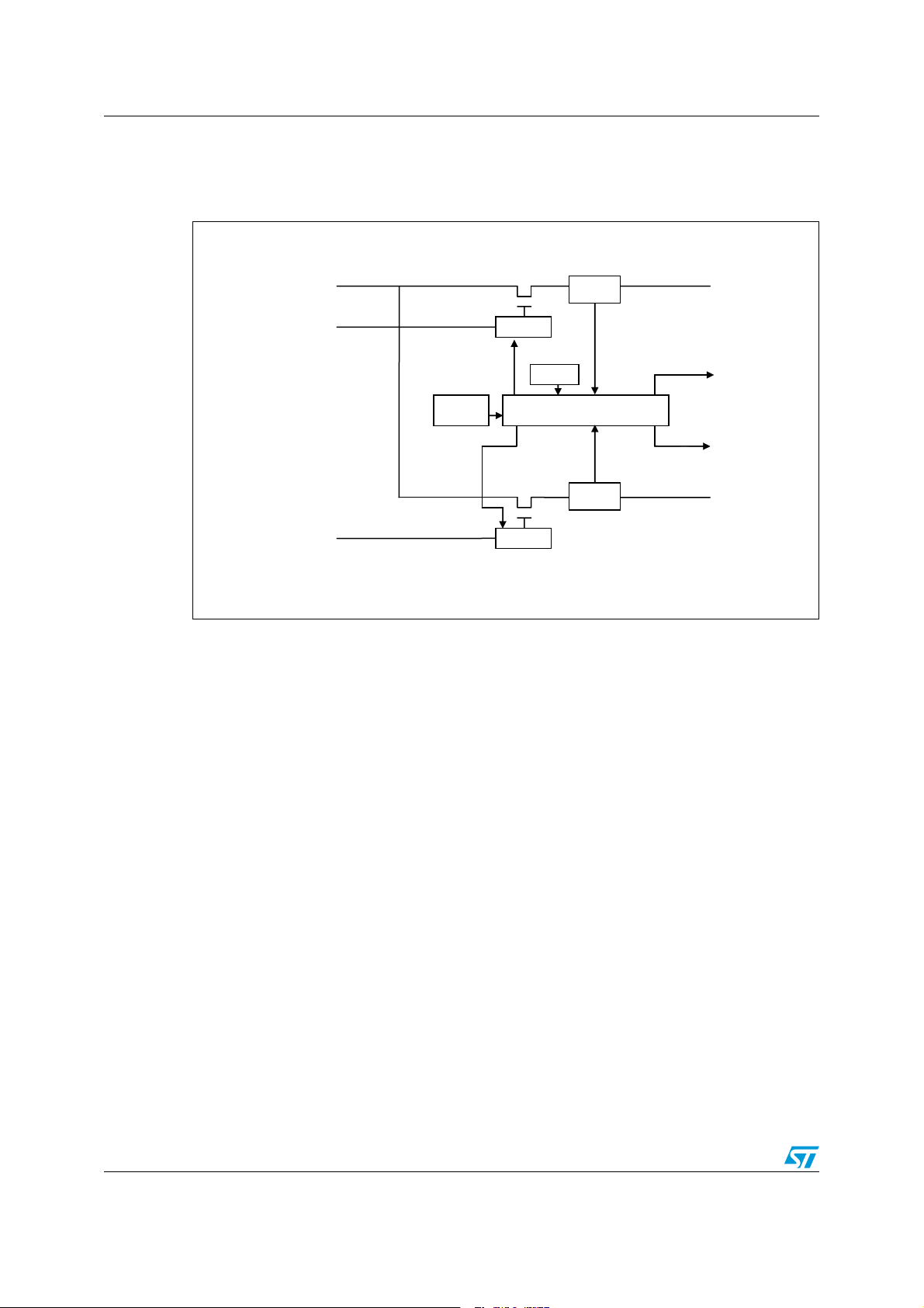
1 Block diagram
Figure 1. Block diagram
).
%.
%.
$RIVER
4HERMAL
SENSE
$RIVER
#URRENT
SENSE
56,/
&AULTBLANKINGREPORTING
DRIVERCONTROLUNIT
#URRENT
SENSE
/54
/#
/#
/54
!-6
6/42 Doc ID 15050 Rev 3
STMPS2242, STMPS2252, STMPS2262, STMPS2272 Pin descriptions
2 Pin descriptions
Figure 2. Pinout
GND
IN
EN1
EN2
Table 2. Pin descriptions
Pin number Name Type Function
1GND
2IN
3EN1/EN1 I
4EN2
5OC2
6OUT2
7OUT1
8OC1
/EN2 I
1
2
3
4
− Ground
− V
O Open drain output for fault indication of channel 2
CC
Channel 1 active low (STMPS2242 and STMPS2262)
or active high (STMPS2252 and STMPS2272) enable
Channel 2 active low (STMPS2242 and STMPS2262)
or active high (STMPS2252 and STMPS2272) enable
− Output of channel 2
− Output of channel 1
O Open drain output for fault indication of channel 1
8
7
6
5
input, 2.7 - 5.5 V
OC1
OUT1
OUT2
OC2
Doc ID 15050 Rev 3 7/42

Functional description STMPS2242, STMPS2252, STMPS2262, STMPS2272
3 Functional description
3.1 Fault blanking
The STMPS devices feature a 10 ms fault blanking. Fault blanking allows current-limit faults,
including momentary short-circuit faults that occur when hot-swapping a capacitive load,
and also ensures that no fault is issued during power-up. When a load transient causes the
device to enter current limit, an internal counter starts. If the load fault persists beyond the
10 ms fault-blanking timeout, the FAULT output asserts “low”. Load-transient faults less than
10 ms (typ.) do not cause a FAULT output assertion. Only current-limit faults have faultblanking. Die overtemperature faults and input voltage drops below the UVLO threshold
cause an immediate fault output.
3.2 Overcurrent/overtemperature protection
In overcurrent or short-circuit condition, the switch limits the current at 500 mA for
STMPS2242/STMPS2252 and 1000 mA for STMPS2262/STMPS2272. If the temperature
of the die goes above the limit value, the switch turns OFF.
3.3 Reverse current blocking
When the switch is OFF, or when the STMPS device is not powered (VCC=0 V), the switch
behaves as a Hi-Z at the output pin, ensuring that no reverse current will flow into the device
when V
Note: In the case where the switch is ON, and a voltage higher than V
reverse current will occur.
I<VO
.
3.4 UVLO
When the input voltage drops below the threshold value, the power switch turns OFF to
prevent improper operation due to low voltage.
is applied to the OUT pin, a
I
8/42 Doc ID 15050 Rev 3
STMPS2242, STMPS2252, STMPS2262, STMPS2272 Maximum rating
4 Maximum rating
Stressing the device above the rating listed in the absolute maximum ratings table may
cause permanent damage to the device. These are stress ratings only and operation of the
device at these or any other conditions above those indicated in the operating sections of
this specification is not implied. Exposure to absolute maximum rating conditions for
extended periods may affect device reliability.
4.1 Absolute maximum rating
Table 3. Absolute maximum ratings
Symbol Parameter Value Unit
V
V
V
O
IENx
I
O
Input voltage range –0.3 – 6.0 V
I
Output voltage range –0.3 – (VI+0.3) V
EN input voltage range –0.3 – 6.0 V
Continuous output current Internally limited
ESD ESD protection level 8 kV
T
T
STG
T
R
T
R
Junction operating temperature –40 to 125 °C
J
Storage temperature –55 to 150 °C
Thermal resistance (MSOP8) 220 °C/W
Thermal resistance (SO-8) 160 °C/W
4.2 Recommended operating conditions
Table 4. Recommended operating conditions
Symbol Parameter
V
I
V
O
I
O
(STMPS2242
STMPS2252)
I
O
(STMPS2262
STMPS2272)
Input voltage 2.7 5.0 5.5 V
Output voltage 0 5.0 5.5 V
Continuous output current 0 - 500 mA
Continuous output current 0 - 1000 mA
Val ue
Unit
Min Typ Max
Doc ID 15050 Rev 3 9/42
Electrical specifications STMPS2242, STMPS2252, STMPS2262, STMPS2272
5 Electrical specifications
Table 5. Electrical characteristics
Val ue
Symbol Parameter Test conditions
=2.7V
V
I
= 25°C
T
Rds(on)
Rds(on)
Static drain source
ON state resistance
Static drain source
ON state resistance
Output rise time
(STMPS2242,STMPS2252)
t
r
Output rise time
(STMPS2262,STMPS2272)
Output fall time
(STMPS2242,STMPS2252)
t
f
Output fall time
(STMPS2262,STMPS2272
Table 6. Current limit characteristics
(V
= 5.5 V, IO= rated current, TJ= 25°C, unless otherwise specified)
I
J
=5.0V
V
I
= 25°C;
T
J
=2.7V
V
I
=5.0V
I
=5.0V
I
LOAD
LOAD
=5.0V
I
LOAD
LOAD
<125°C
J
<125°C
J
=10Ω
=1µF
=10Ω
=1µF
-40 < T
V
-40 < T
V
R
C
V
R
C
VI=5.0V
R
=10Ω
LOAD
=1µF
C
LOAD
V
=5.0V
I
=10Ω
R
LOAD
=1µF
C
LOAD
Symbol Parameter Test condition
Min Typ Max
120 160 mΩ
105 115 mΩ
200
140
0.05 2 ms
0.05 2 ms
0.05 2 ms
0.05 2 ms
Val ue
Min Typ Max
Unit
mΩ
Unit
I
OS
(STMPS2242
STMPS2252)
IOS
(STMPS2262
STMPS2272)
Short circuit output
current
V
=5V
I
OUT connected to
GND through 10 mΩ
load, device enabled
into short circuit
10/42 Doc ID 15050 Rev 3
0.6 0.8 1.0 A
1.1 1.6 2.0 A
STMPS2242, STMPS2252, STMPS2262, STMPS2272 Electrical specifications
Table 7. Supply current characteristics
(V
= 5.5 V, IO= rated current, TJ= 25°C, unless otherwise specified)
I
Val ue
Symbol Parameter Test condition
Min Typ Max
Unit
1. I
I
off
I
on
I
leakage
I
reverse
leakage
Switch turned off
Switch turned on
Output leakage
current
Reversed leakage
current
= I
off-ground
- I
(1)
, where I
off
No load
Switch is off
No load
Switch is off
-40 < TJ< 125°C
No load
Switch is on
No load
Switch is on
-40 < TJ< 125°C
I
off (grounded output)
I
off (floating output)
I
off (grounded output)
I
off (floating output)
-
-
-40 < TJ< 125°C
Switch is off
< VO,
V
I
Output connected to
5.5 V, 25°C
Switch is off
VI < V
O
Output connected to
5.5 V, 125°C
= current into IN when switch is off and output is grounded
off-ground
914
μA
16
50 70
μA
85
12
μA
16
12
μA
110
Table 8. Thermal characteristics
(V
= 5.5 V, IO= rated current, TJ= 25°C, unless otherwise specified)
I
Val ue
Symbol Parameter Test condition
Min Typ Max
T1
T2
Thermal shutdown
threshold
Recovery from
thermal shutdown
135 °C
125 °C
Hysteresis 10 °C
Doc ID 15050 Rev 3 11/42
Unit
Electrical specifications STMPS2242, STMPS2252, STMPS2262, STMPS2272
Table 9. UVLO characteristics
(V
= 5.5 V, IO= rated current, TJ= 25°C, unless otherwise specified)
I
Val ue
Symbol Parameter Test condition
Min Typ Max
Unit
V
UVLO
Undervoltage lockout
threshold
2.0 2.5 V
Hysteresis 75 mV
Table 10. OCx pin characteristics
(V
= 5.5 V, IO= rated current, TJ= 25°C, unless otherwise specified)
I
Val ue
Symbol Parameter Test condition
Min Typ Max
OC blanking
V
O
I
off
Table 11. ENx pin characteristics
OCx assertion and
de-assertion
4815ms
Output low voltage IO=5mA −−0.4 V
Off current
(V
= 5.5 V, IO= rated current, TJ= 25°C, unless otherwise specified)
I
VOC = 2.7V, 5.5V
(No OC condition)
−−1.0 µA
Val ue
Symbol Parameter Test condition
Min Typ Max
V
IH
High level input
voltage
V
= 2.7 V to 5.5 V 2.0 −−V
I
Unit
Unit
= 4.5 V to 5.5 V −−0.8 V
V
V
IL
I
I
t
on
t
off
1. Not tested in production, specified by design.
Low level input
voltage
Input current V
Turn ON time
Turn OFF time
(1)
(1)
I
= 2.7 V to 4.5 V −−0.4 V
V
I
=0V or V
IENx
R
=10Ω
LOAD
C
= 100 μF
LOAD
R
=10Ω
LOAD
= 100 μF
C
LOAD
12/42 Doc ID 15050 Rev 3
I
-0.5 − 0.5 µA
−−5ms
−−10 ms
STMPS2242, STMPS2252, STMPS2262, STMPS2272 Typical operating characteristics
6 Typical operating characteristics
6.1 STMPS2242, STMPS2252 characteristics
The waveforms and characteristics shown in this section pertain to the STMPS2252 device.
The STMPS2242 is expected to have the same characteristics with inverted EN input
function. All measurements are at ambient temperature 25 °C.
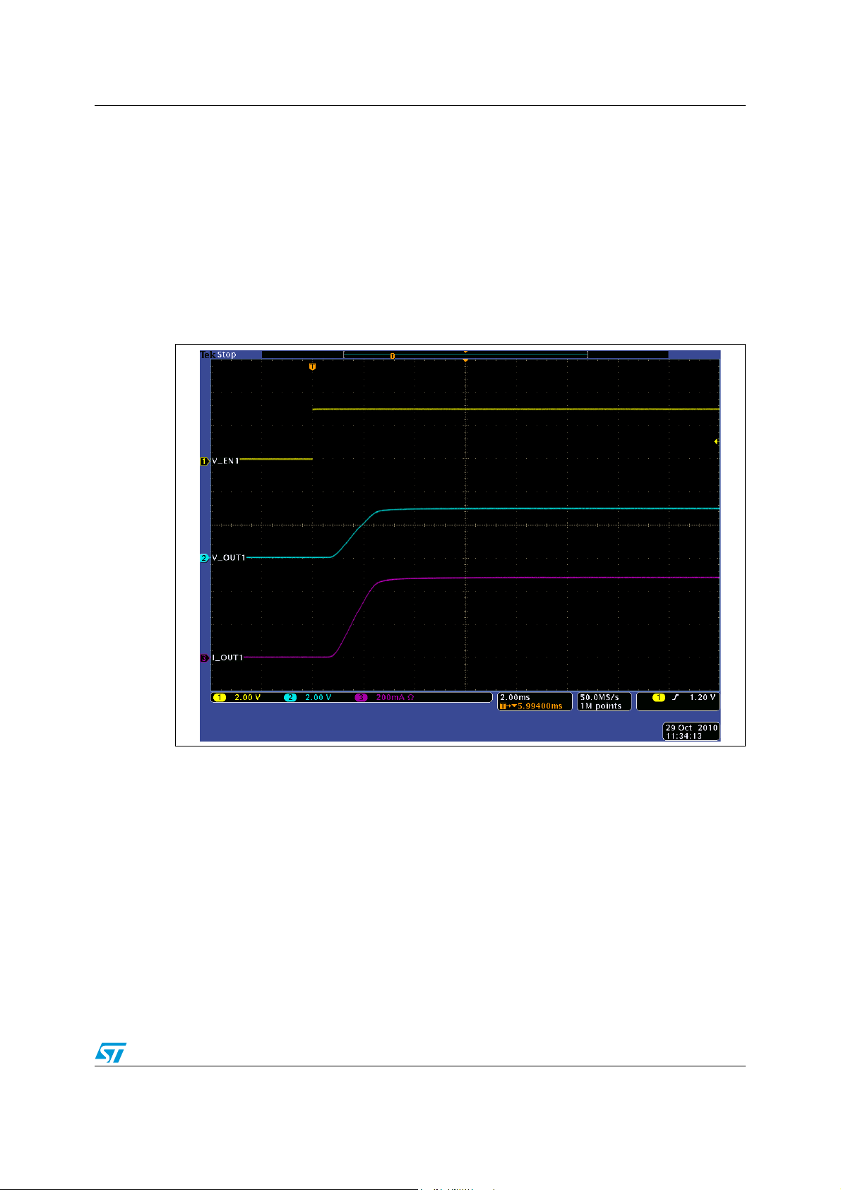
6.1.1 Turn-on/off characteristics for VI = 3 V, R
Figure 3. Turn-on for C
LOAD
= 1 µF
LOAD
= 6 Ω
Doc ID 15050 Rev 3 13/42

Typical operating characteristics STMPS2242, STMPS2252, STMPS2262, STMPS2272
Figure 4. Turn-on for C
LOAD
= 100 µF
Figure 5. Turn-on for C
LOAD
= 470 µF
14/42 Doc ID 15050 Rev 3

STMPS2242, STMPS2252, STMPS2262, STMPS2272 Typical operating characteristics
Figure 6. Turn-off for C
LOAD
= 1 µF
Figure 7. Turn-off for C
LOAD
= 100 µF
Doc ID 15050 Rev 3 15/42

Typical operating characteristics STMPS2242, STMPS2252, STMPS2262, STMPS2272
Figure 8. Turn-off for C
LOAD
= 470 µF
6.1.2 Turn-on/off characteristics for VI = 5 V, R
Figure 9. Turn-on for C
LOAD
= 1 µF
LOAD
= 10 Ω
16/42 Doc ID 15050 Rev 3

STMPS2242, STMPS2252, STMPS2262, STMPS2272 Typical operating characteristics
Figure 10. Turn-on for C
LOAD
= 100 µF
Figure 11. Turn-on for C
LOAD
= 470 µF
Doc ID 15050 Rev 3 17/42

Typical operating characteristics STMPS2242, STMPS2252, STMPS2262, STMPS2272
Figure 12. Turn-off for C
LOAD
= 1 µF
Figure 13. Turn-off for C
LOAD
= 100 µF
18/42 Doc ID 15050 Rev 3

STMPS2242, STMPS2252, STMPS2262, STMPS2272 Typical operating characteristics
Figure 14. Turn-off for C
LOAD
= 470 µF
Doc ID 15050 Rev 3 19/42

Typical operating characteristics STMPS2242, STMPS2252, STMPS2262, STMPS2272
6.1.3 UVLO characteristics
Figure 15. UVLO, VI rising
Figure 16. UVLO, V
falling
I
20/42 Doc ID 15050 Rev 3

STMPS2242, STMPS2252, STMPS2262, STMPS2272 Typical operating characteristics
6.1.4 Overcurrent protection characteristics
Figure 17. Overcurrent protection characteristics, VI = 3 V, R
LOAD
= 2.2 Ω
Figure 18. Overcurrent protection characteristics, V
= 5 V, R
I
LOAD
= 2.2 Ω
Doc ID 15050 Rev 3 21/42

Typical operating characteristics STMPS2242, STMPS2252, STMPS2262, STMPS2272
6.1.5 Other electrical characteristics
Figure 19. ICC versus V
60
50
40
30
(µA)
CC
I
20
10
0
23456
Figure 20. tr versus V
5.0
4.5
4.0
3.5
3.0
2.5
(m s)
r
t
2.0
1.5
1.0
0.5
0.0
0123456
I
I
EN = H
EN = L
VI (V)
AM045006v1
C
= 1 µF or
L OAD
100 µF
C
= 470 µF
L OAD
VI (V)
AM045007v1
22/42 Doc ID 15050 Rev 3

STMPS2242, STMPS2252, STMPS2262, STMPS2272 Typical operating characteristics
Figure 21. tf versus V
I
14
12
10
8
(m s )
f
6
t
4
2
0
0123456
Figure 22. Rds(on) versus V
130
C
= 1 µF
L OAD
C
= 100 µF
L OAD
C
= 470 µF
L OAD
VI (V)
AM045008v1
I
120
110
100
90
Rds(on) (mΩ)
80
70
60
2 2.5 3 3.5 4 4.5 5 5.5 6
VI (V)
AM045009v1
Doc ID 15050 Rev 3 23/42

Typical operating characteristics STMPS2242, STMPS2252, STMPS2262, STMPS2272
6.2 STMPS2262, STMPS2272 characteristics
The waveforms and characteristics shown in this section pertain to the STMPS2272 device.
The STMPS2262 is expected to have the same characteristics with inverted EN input
function. All measurements are at ambient temperature 25 °C.
6.2.1 Turn-on/off characteristics for VI = 3 V, R
Figure 23. Turn-on for C
LOAD
= 1 µF
LOAD
= 3 Ω
24/42 Doc ID 15050 Rev 3

STMPS2242, STMPS2252, STMPS2262, STMPS2272 Typical operating characteristics
Figure 24. Turn-on for C
LOAD
= 100 µF
Figure 25. Turn-on for C
LOAD
= 470 µF
Doc ID 15050 Rev 3 25/42

Typical operating characteristics STMPS2242, STMPS2252, STMPS2262, STMPS2272
Figure 26. Turn-off for C
LOAD
= 1 µF
Figure 27. Turn-off for C
LOAD
= 100 µF
26/42 Doc ID 15050 Rev 3

STMPS2242, STMPS2252, STMPS2262, STMPS2272 Typical operating characteristics
Figure 28. Turn-off for C
LOAD
= 470 µF
6.2.2 Turn-on/off characteristics for VI = 5 V, R
Figure 29. Turn-on for C
LOAD
= 1 µF
LOAD
= 5 Ω
Doc ID 15050 Rev 3 27/42

Typical operating characteristics STMPS2242, STMPS2252, STMPS2262, STMPS2272
Figure 30. Turn-on for C
LOAD
= 100 µF
Figure 31. Turn-on for C
LOAD
= 470 µF
28/42 Doc ID 15050 Rev 3

STMPS2242, STMPS2252, STMPS2262, STMPS2272 Typical operating characteristics
Figure 32. Turn-off for C
LOAD
= 1 µF
Figure 33. Turn-off for C
LOAD
= 100 µF
Doc ID 15050 Rev 3 29/42

Typical operating characteristics STMPS2242, STMPS2252, STMPS2262, STMPS2272
Figure 34. Turn-off for C
LOAD
= 470 µF
6.2.3 UVLO characteristics
Figure 35. UVLO, VI rising
30/42 Doc ID 15050 Rev 3

STMPS2242, STMPS2252, STMPS2262, STMPS2272 Typical operating characteristics
Figure 36. UVLO, VI falling
Doc ID 15050 Rev 3 31/42

Typical operating characteristics STMPS2242, STMPS2252, STMPS2262, STMPS2272
6.2.4 Overcurrent protection characteristics
Figure 37. Overcurrent protection characteristics, VI = 3 V, R
LOAD
= 1 Ω
Figure 38. Overcurrent protection characteristics, V
= 5 V, R
I
LOAD
= 1 Ω
32/42 Doc ID 15050 Rev 3

STMPS2242, STMPS2252, STMPS2262, STMPS2272 Typical operating characteristics
6.2.5 Other electrical characteristics
Figure 39. ICC versus V
60
50
40
30
(µA)
CC
I
20
10
0
23456
Figure 40. tr versus V
3
2.5
I
I
EN = H
EN = L
VI (V)
AM045026v1
2
1.5
(m s)
r
t
1
0.5
0
0123456
VI (V)
C
= 1 µF or
L OAD
100 µF
C
= 470 µF
L OAD
AM045024v1
Doc ID 15050 Rev 3 33/42

Typical operating characteristics STMPS2242, STMPS2252, STMPS2262, STMPS2272
Figure 41. tf versus V
I
7
6
5
4
(m s )
f
3
t
2
1
0
0123456
VI (V)
Figure 42. Rds(on) versus V
I
130
C
C
C
L OAD
L OAD
L OAD
= 1 µF
= 100 µF
= 470 µF
AM045028v1
120
110
100
90
Rds(on) (mΩ)
80
70
60
2 2.5 3 3.5 4 4.5 5 5.5 6
VI (V)
AM045029v1
34/42 Doc ID 15050 Rev 3

STMPS2242, STMPS2252, STMPS2262, STMPS2272 Application information
7 Application information
7.1 Input and output capacitors
Input and output capacitors improve the performance of the device; the actual capacitance
should be optimized for the particular application. For all applications, a 0.1 µF or greater
ceramic bypass capacitor between IN and GND as close to the device as possible is
recommended for local noise decoupling. This precaution also reduces ringing on the input
due to power supply transients.
An additional capacitor may be needed on the input to reduce input voltage overshoots from
exceeding the absolute maximum voltage of the device during heavy transient conditions.
This is especially important during bench testing when long, inductive cables are used to
connect the evaluation board to the bench power supply. The value of 100 µF may be
adequate in most situations.
An output capacitor is not required for device functionality, but placing a high-value (in the
order of 10 - 100 µF) electrolytic capacitor on the output pins is recommended when large
transient currents are expected on the output.
Doc ID 15050 Rev 3 35/42

Package mechanical data STMPS2242, STMPS2252, STMPS2262, STMPS2272
8 Package mechanical data
In order to meet environmental requirements, ST offers these devices in different grades of
ECOPACK
specifications, grade definitions and product status are available at: www.st.com.
ECOPACK
®
packages, depending on their level of environmental compliance. ECOPACK®
®
is an ST trademark.
Figure 43. SO-8 package outline
36/42 Doc ID 15050 Rev 3
0016023 C

STMPS2242, STMPS2252, STMPS2262, STMPS2272 Package mechanical data
Table 12. SO-8 mechanical data
Millimeters
Symbol
Min Typ Max
A 1.35
A1 0.10
A2 1.10
B 0.33
C 0.19
(1)
D
E 3.80
e
H 5.80 − 6.20
h 0.25
L 0.40
k 0° (min.), 8° (max.)
ddd −−0.10
1. Dimension D does not include mold flash, protrusions or gate burrs. Mold flash, potrusions or gate burrs
shall not exceed 0.15 mm (0.006 inch) in total (both sides).
4.80 − 5.00
− 1.27 −
− 1.75
− 0.25
− 1.65
− 0.51
− 0.25
− 4.00
− 0.50
− 1.27
Doc ID 15050 Rev 3 37/42

Package mechanical data STMPS2242, STMPS2252, STMPS2262, STMPS2272
Figure 44. MSOP8 package outline
Table 13. MSOP8 mechanical data
Symbol
Min Typ Max
A
A1 0
A2 0.75 0.85 0.95
b 0.22 − 0.40
c 0.08
D 2.90 3.00 3.10
D3
E 4.67 4.90 5.07
E1 2.90 3.00 3.10
E5
e − 0.65
e1 1.95 −
L 0.40 − 0.80
−−1.10
− 2.16 −
− 1.73 −
MSOP8_7277133_C
Millimeters
− 0.15
− 0.23
−
L2
< 0° − 6°
38/42 Doc ID 15050 Rev 3
− 0.25 −

STMPS2242, STMPS2252, STMPS2262, STMPS2272 Package mechanical data
Figure 45. SO-8 carrier tape
Figure 46. MSOP8 carrier tape
0010914_G
?"
Doc ID 15050 Rev 3 39/42

Package mechanical data STMPS2242, STMPS2252, STMPS2262, STMPS2272
Figure 47. Reel information
Table 14. Reel mechanical data
Symbol
Min Typ Max
A 330
C 12.8 13.2
D 20.2
N60
T 22.4
Millimeters
40/42 Doc ID 15050 Rev 3

STMPS2242, STMPS2252, STMPS2262, STMPS2272 Revision history
9 Revision history
Table 15. Document revision history
Date Revision Changes
03-Dec-2008 1 Initial release.
18-Dec-2009 2 Modified: Ta b le 6, Ta bl e 7 and Ta b le 9 .
19-Jan-2011 3
Added Section 6: Typical operating characteristics and Section 7:
Application information; minor textual changes.
Doc ID 15050 Rev 3 41/42

STMPS2242, STMPS2252, STMPS2262, STMPS2272
Please Read Carefully:
Information in this document is provided solely in connection with ST products. STMicroelectronics NV and its subsidiaries (“ST”) reserve the
right to make changes, corrections, modifications or improvements, to this document, and the products and services described herein at any
time, without notice.
All ST products are sold pursuant to ST’s terms and conditions of sale.
Purchasers are solely responsible for the choice, selection and use of the ST products and services described herein, and ST assumes no
liability whatsoever relating to the choice, selection or use of the ST products and services described herein.
No license, express or implied, by estoppel or otherwise, to any intellectual property rights is granted under this document. If any part of this
document refers to any third party products or services it shall not be deemed a license grant by ST for the use of such third party products
or services, or any intellectual property contained therein or considered as a warranty covering the use in any manner whatsoever of such
third party products or services or any intellectual property contained therein.
UNLESS OTHERWISE SET FORTH IN ST’S TERMS AND CONDITIONS OF SALE ST DISCLAIMS ANY EXPRESS OR IMPLIED
WARRANTY WITH RESPECT TO THE USE AND/OR SALE OF ST PRODUCTS INCLUDING WITHOUT LIMITATION IMPLIED
WARRANTIES OF MERCHANTABILITY, FITNESS FOR A PARTICULAR PURPOSE (AND THEIR EQUIVALENTS UNDER THE LAWS
OF ANY JURISDICTION), OR INFRINGEMENT OF ANY PATENT, COPYRIGHT OR OTHER INTELLECTUAL PROPERTY RIGHT.
UNLESS EXPRESSLY APPROVED IN WRITING BY AN AUTHORIZED ST REPRESENTATIVE, ST PRODUCTS ARE NOT
RECOMMENDED, AUTHORIZED OR WARRANTED FOR USE IN MILITARY, AIR CRAFT, SPACE, LIFE SAVING, OR LIFE SUSTAINING
APPLICATIONS, NOR IN PRODUCTS OR SYSTEMS WHERE FAILURE OR MALFUNCTION MAY RESULT IN PERSONAL INJURY,
DEATH, OR SEVERE PROPERTY OR ENVIRONMENTAL DAMAGE. ST PRODUCTS WHICH ARE NOT SPECIFIED AS "AUTOMOTIVE
GRADE" MAY ONLY BE USED IN AUTOMOTIVE APPLICATIONS AT USER’S OWN RISK.
Resale of ST products with provisions different from the statements and/or technical features set forth in this document shall immediately void
any warranty granted by ST for the ST product or service described herein and shall not create or extend in any manner whatsoever, any
liability of ST.
ST and the ST logo are trademarks or registered trademarks of ST in various countries.
Information in this document supersedes and replaces all information previously supplied.
The ST logo is a registered trademark of STMicroelectronics. All other names are the property of their respective owners.
© 2011 STMicroelectronics - All rights reserved
STMicroelectronics group of companies
Australia - Belgium - Brazil - Canada - China - Czech Republic - Finland - France - Germany - Hong Kong - India - Israel - Italy - Japan -
Malaysia - Malta - Morocco - Philippines - Singapore - Spain - Sweden - Switzerland - United Kingdom - United States of America
www.st.com
42/42 Doc ID 15050 Rev 3
 Loading...