

Enhanced single channel power switches
Features
■ 90 mΩ high-side MOSFET switch
■ 500/1000 mA continuous current
■ Thermal and short-circuit protection with
overcurrent logic output
■ Operating range from 2.7 V to 5.5 V
■ CMOS- and TTL-compatible enable inputs
■ Undervoltage lockout (UVLO)
■ 12 µA maximum standby supply current
■ Ambient temperature range, -40°C to 85°C
■ 8 kV ESD protection
■ Reverse current protection
■ Fault-blanking
STMPS2141, STMPS2151
STMPS2161, STMPS2171
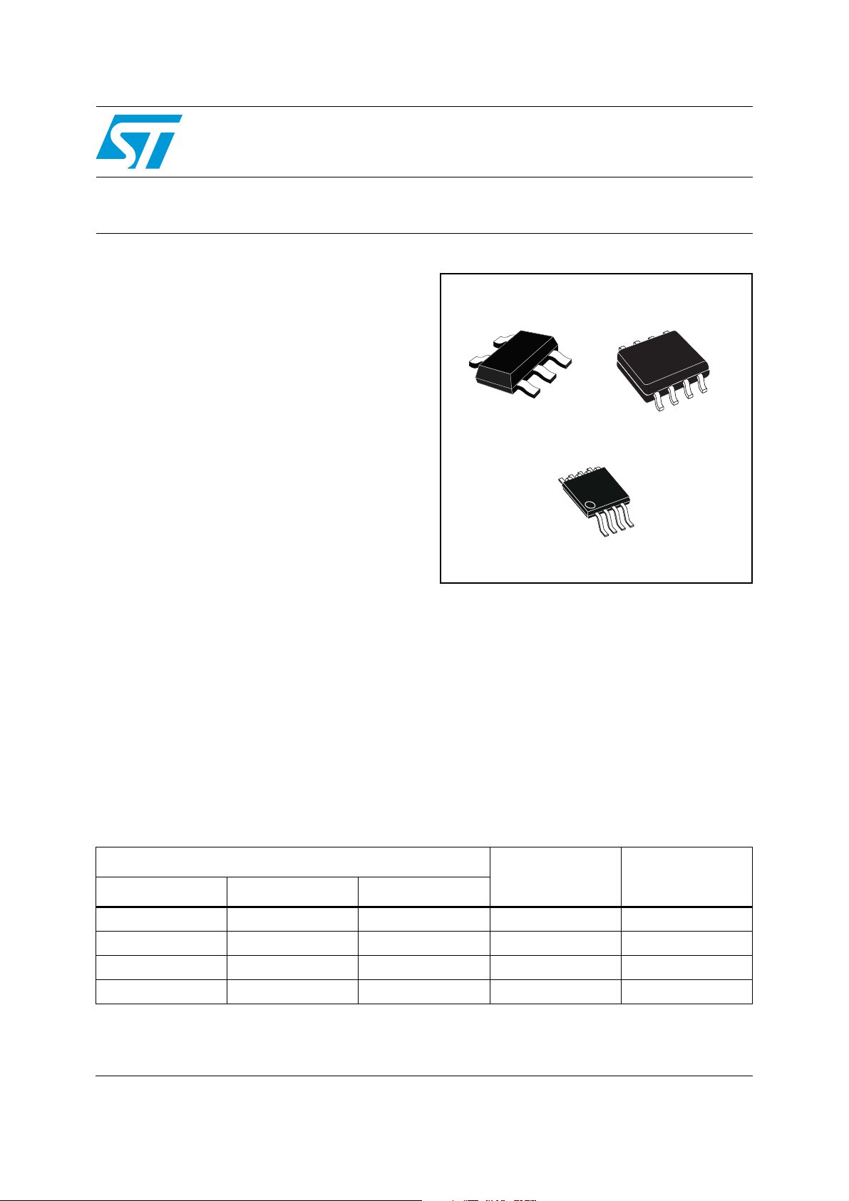
SOT23-5L
MSOP8
SO-8
Description
The STMPS2141, STMPS2151, STMPS2161,
STMPS2171 power distribution switches are
intended for applications where heavy capacitive
loads and short circuits are likely to be
encountered. These devices incorporate 90 mΩ
N-channel MOSFET high-side power switches for
power-distribution. These switches are controlled
by a logic enable input.
When the output load exceeds the current-limit
threshold or a short is present, the device limits
the output current to a safe level by switching into
a constant-current mode. When continuous heavy
overloads and short circuits increase the power
dissipation in the switch, causing the junction
temperature to rise, a thermal protection circuit
shuts the switch off to prevent damage. Recovery
from a thermal shutdown is automatic once the
device has cooled sufficiently. Internal circuitry
ensures the switch remains off until a valid input
voltage is present.
Table 1. Device summary
Order codes
SO-8 SOT23-5L MSOP8
STMPS2141MTR STMPS2141STR STMPS2141TTR 500 Active low
STMPS2151MTR STMPS2151STR STMPS2151TTR 500 Active high
STMPS2161MTR STMPS2161STR STMPS2161TTR 1000 Active low
STMPS2171MTR STMPS2171STR STMPS2171TTR 1000 Active high
1. MSOP8 package is also known as “TSSOP8”
(1)
Current limit
(mA)
Enable
July 2009 Doc ID 13793 Rev 4 1/34
www.st.com
34

Contents STMPS2141, STMPS2151, STMPS2161, STMPS2171
Contents
1 Block diagram . . . . . . . . . . . . . . . . . . . . . . . . . . . . . . . . . . . . . . . . . . . . . . 7
2 Pin settings . . . . . . . . . . . . . . . . . . . . . . . . . . . . . . . . . . . . . . . . . . . . . . . . 8
2.1 Pin connections . . . . . . . . . . . . . . . . . . . . . . . . . . . . . . . . . . . . . . . . . . . . . 8
2.2 Pin description . . . . . . . . . . . . . . . . . . . . . . . . . . . . . . . . . . . . . . . . . . . . . . 8
3 Functional description . . . . . . . . . . . . . . . . . . . . . . . . . . . . . . . . . . . . . . . 9
3.1 Fault blanking . . . . . . . . . . . . . . . . . . . . . . . . . . . . . . . . . . . . . . . . . . . . . . . 9
3.2 Overcurrent/over-temperature protection . . . . . . . . . . . . . . . . . . . . . . . . . . 9
3.3 FAULT conditions . . . . . . . . . . . . . . . . . . . . . . . . . . . . . . . . . . . . . . . . . . . . 9
3.4 Reversed current blocking . . . . . . . . . . . . . . . . . . . . . . . . . . . . . . . . . . . . 10
3.5 UVLO . . . . . . . . . . . . . . . . . . . . . . . . . . . . . . . . . . . . . . . . . . . . . . . . . . . . 10
4 Ambient temperature . . . . . . . . . . . . . . . . . . . . . . . . . . . . . . . . . . . . . . . 11
5 Maximum ratings . . . . . . . . . . . . . . . . . . . . . . . . . . . . . . . . . . . . . . . . . . . 12
5.1 Absolute maximum ratings . . . . . . . . . . . . . . . . . . . . . . . . . . . . . . . . . . . . 12
5.2 Recommended operating conditions . . . . . . . . . . . . . . . . . . . . . . . . . . . . 12
6 Electrical specifications . . . . . . . . . . . . . . . . . . . . . . . . . . . . . . . . . . . . . 13
7 Detail device characteristics . . . . . . . . . . . . . . . . . . . . . . . . . . . . . . . . . 16
7.1 STMPS2141, STMPS2151 additional electrical charts . . . . . . . . . . . . . . 16
7.1.1 Turn on/off characteristics at VOUT = 5.0 V . . . . . . . . . . . . . . . . . . . . . 16
7.1.2 Turn on/off characteristics at VOUT = 3.0 V . . . . . . . . . . . . . . . . . . . . . 17
7.1.3 UVLO . . . . . . . . . . . . . . . . . . . . . . . . . . . . . . . . . . . . . . . . . . . . . . . . . . . 17
7.1.4 OC protection characteristics . . . . . . . . . . . . . . . . . . . . . . . . . . . . . . . . 18
7.1.5 Other electrical characteristics . . . . . . . . . . . . . . . . . . . . . . . . . . . . . . . . 18
7.2 STMPS2161, STMPS2171 electrical charts . . . . . . . . . . . . . . . . . . . . . . 21
7.2.1 Turn on/off characteristics at VOUT = 5.0 V . . . . . . . . . . . . . . . . . . . . . 21
7.2.2 Turn on/off characteristics at VOUT = 3.0 V . . . . . . . . . . . . . . . . . . . . . 22
7.2.3 UVLO . . . . . . . . . . . . . . . . . . . . . . . . . . . . . . . . . . . . . . . . . . . . . . . . . . . 22
7.2.4 OC protection characteristics . . . . . . . . . . . . . . . . . . . . . . . . . . . . . . . . 23
7.2.5 Other electrical characteristics . . . . . . . . . . . . . . . . . . . . . . . . . . . . . . . . 24
2/34 Doc ID 13793 Rev 4

STMPS2141, STMPS2151, STMPS2161, STMPS2171 Contents
8 Package mechanical data . . . . . . . . . . . . . . . . . . . . . . . . . . . . . . . . . . . . 26
9 Revision history . . . . . . . . . . . . . . . . . . . . . . . . . . . . . . . . . . . . . . . . . . . 33
Doc ID 13793 Rev 4 3/34

List of figures STMPS2141, STMPS2151, STMPS2161, STMPS2171
List of figures
Figure 1. Block diagram . . . . . . . . . . . . . . . . . . . . . . . . . . . . . . . . . . . . . . . . . . . . . . . . . . . . . . . . . . . . 6
Figure 2. SOT23-5L, SO-8 and MSOP8 pin connections . . . . . . . . . . . . . . . . . . . . . . . . . . . . . . . . . . 7
Figure 3. Voltage output turn on delay time . . . . . . . . . . . . . . . . . . . . . . . . . . . . . . . . . . . . . . . . . . . . 15
Figure 4. Voltage output turn off delay time . . . . . . . . . . . . . . . . . . . . . . . . . . . . . . . . . . . . . . . . . . . . 15
Figure 5. Current output turn on delay time . . . . . . . . . . . . . . . . . . . . . . . . . . . . . . . . . . . . . . . . . . . . 15
Figure 6. Current output turn off delay time . . . . . . . . . . . . . . . . . . . . . . . . . . . . . . . . . . . . . . . . . . . . 15
Figure 7. Voltage output turn on delay time . . . . . . . . . . . . . . . . . . . . . . . . . . . . . . . . . . . . . . . . . . . . 16
Figure 8. Voltage output turn off delay time . . . . . . . . . . . . . . . . . . . . . . . . . . . . . . . . . . . . . . . . . . . . 16
Figure 9. Current output turn on delay time . . . . . . . . . . . . . . . . . . . . . . . . . . . . . . . . . . . . . . . . . . . . 16
Figure 10. Current output turn off delay time . . . . . . . . . . . . . . . . . . . . . . . . . . . . . . . . . . . . . . . . . . . . 16
Figure 11. UVLO rising . . . . . . . . . . . . . . . . . . . . . . . . . . . . . . . . . . . . . . . . . . . . . . . . . . . . . . . . . . . . 16
Figure 12. UVLO falling . . . . . . . . . . . . . . . . . . . . . . . . . . . . . . . . . . . . . . . . . . . . . . . . . . . . . . . . . . . . 16
Figure 13. OC protection at VOUT = 3.0 V . . . . . . . . . . . . . . . . . . . . . . . . . . . . . . . . . . . . . . . . . . . . . 17
Figure 14. OC protection at VOUT = 3.0 V . . . . . . . . . . . . . . . . . . . . . . . . . . . . . . . . . . . . . . . . . . . . . 17
Figure 15. OC protection at VOUT = 5.0 V . . . . . . . . . . . . . . . . . . . . . . . . . . . . . . . . . . . . . . . . . . . . . 17
Figure 16. OC protection at VOUT = 5.0 V . . . . . . . . . . . . . . . . . . . . . . . . . . . . . . . . . . . . . . . . . . . . . 17
Figure 17. ICC vs VIN (enabled) . . . . . . . . . . . . . . . . . . . . . . . . . . . . . . . . . . . . . . . . . . . . . . . . . . . . . 17
Figure 18. ICC vs temperature (enabled) . . . . . . . . . . . . . . . . . . . . . . . . . . . . . . . . . . . . . . . . . . . . . . 17
Figure 19. ICC vs VIN (disabled) . . . . . . . . . . . . . . . . . . . . . . . . . . . . . . . . . . . . . . . . . . . . . . . . . . . . . 18
Figure 20. ICC vs temperature (disabled) . . . . . . . . . . . . . . . . . . . . . . . . . . . . . . . . . . . . . . . . . . . . . . 18
Figure 21. RDS ON vs VIN . . . . . . . . . . . . . . . . . . . . . . . . . . . . . . . . . . . . . . . . . . . . . . . . . . . . . . . . . 18
Figure 22. RDS ON vs temperature . . . . . . . . . . . . . . . . . . . . . . . . . . . . . . . . . . . . . . . . . . . . . . . . . . . 18
Figure 23. ILIMIT vs temperature. . . . . . . . . . . . . . . . . . . . . . . . . . . . . . . . . . . . . . . . . . . . . . . . . . . . . 18
Figure 24. Switch leakage vs temperature. . . . . . . . . . . . . . . . . . . . . . . . . . . . . . . . . . . . . . . . . . . . . . 18
Figure 25. Output rise time vs. VIN . . . . . . . . . . . . . . . . . . . . . . . . . . . . . . . . . . . . . . . . . . . . . . . . . . . 19
Figure 26. Output fall time vs. VIN . . . . . . . . . . . . . . . . . . . . . . . . . . . . . . . . . . . . . . . . . . . . . . . . . . . . 19
Figure 27. UVLO vs temperature . . . . . . . . . . . . . . . . . . . . . . . . . . . . . . . . . . . . . . . . . . . . . . . . . . . . . 19
Figure 28. Voltage output turn on delay time . . . . . . . . . . . . . . . . . . . . . . . . . . . . . . . . . . . . . . . . . . . . 20
Figure 29. Voltage output turn off delay time . . . . . . . . . . . . . . . . . . . . . . . . . . . . . . . . . . . . . . . . . . . . 20
Figure 30. Current output turn on delay time . . . . . . . . . . . . . . . . . . . . . . . . . . . . . . . . . . . . . . . . . . . . 20
Figure 31. Current output turn off delay time . . . . . . . . . . . . . . . . . . . . . . . . . . . . . . . . . . . . . . . . . . . . 20
Figure 32. Voltage output turn on delay time . . . . . . . . . . . . . . . . . . . . . . . . . . . . . . . . . . . . . . . . . . . . 21
Figure 33. Voltage output turn off delay time . . . . . . . . . . . . . . . . . . . . . . . . . . . . . . . . . . . . . . . . . . . . 21
Figure 34. Current output turn on delay time . . . . . . . . . . . . . . . . . . . . . . . . . . . . . . . . . . . . . . . . . . . . 21
Figure 35. Current output turn off delay time . . . . . . . . . . . . . . . . . . . . . . . . . . . . . . . . . . . . . . . . . . . . 21
Figure 36. UVLO rising . . . . . . . . . . . . . . . . . . . . . . . . . . . . . . . . . . . . . . . . . . . . . . . . . . . . . . . . . . . . 21
Figure 37. UVLO falling . . . . . . . . . . . . . . . . . . . . . . . . . . . . . . . . . . . . . . . . . . . . . . . . . . . . . . . . . . . . 21
Figure 38. OC protection at VOUT = 3.0 V . . . . . . . . . . . . . . . . . . . . . . . . . . . . . . . . . . . . . . . . . . . . . 22
Figure 39. OC protection at VOUT = 3.0 V . . . . . . . . . . . . . . . . . . . . . . . . . . . . . . . . . . . . . . . . . . . . . 22
Figure 40. OC protection at VOUT = 5.0 V . . . . . . . . . . . . . . . . . . . . . . . . . . . . . . . . . . . . . . . . . . . . . 22
Figure 41. OC protection at VOUT = 5.0 V . . . . . . . . . . . . . . . . . . . . . . . . . . . . . . . . . . . . . . . . . . . . . 22
Figure 42. ICC vs VIN (enabled) . . . . . . . . . . . . . . . . . . . . . . . . . . . . . . . . . . . . . . . . . . . . . . . . . . . . . 23
Figure 43. ICC vs temperature (enabled) . . . . . . . . . . . . . . . . . . . . . . . . . . . . . . . . . . . . . . . . . . . . . . 23
Figure 44. ICC vs VIN (disabled) . . . . . . . . . . . . . . . . . . . . . . . . . . . . . . . . . . . . . . . . . . . . . . . . . . . . . 23
Figure 45. ICC vs temperature (disabled) . . . . . . . . . . . . . . . . . . . . . . . . . . . . . . . . . . . . . . . . . . . . . . 23
Figure 46. RDS ON vs VIN . . . . . . . . . . . . . . . . . . . . . . . . . . . . . . . . . . . . . . . . . . . . . . . . . . . . . . . . . 23
Figure 47. RDS ON vs temperature . . . . . . . . . . . . . . . . . . . . . . . . . . . . . . . . . . . . . . . . . . . . . . . . . . . 23
Figure 48. ILIMIT vs temperature. . . . . . . . . . . . . . . . . . . . . . . . . . . . . . . . . . . . . . . . . . . . . . . . . . . . . 24
4/34 Doc ID 13793 Rev 4

STMPS2141, STMPS2151, STMPS2161, STMPS2171 List of figures
Figure 49. Switch leakage vs temperature. . . . . . . . . . . . . . . . . . . . . . . . . . . . . . . . . . . . . . . . . . . . . . 24
Figure 50. Output rise time vs. VIN . . . . . . . . . . . . . . . . . . . . . . . . . . . . . . . . . . . . . . . . . . . . . . . . . . . 24
Figure 51. Output fall time vs. VIN . . . . . . . . . . . . . . . . . . . . . . . . . . . . . . . . . . . . . . . . . . . . . . . . . . . . 24
Figure 52. UVLO vs temperature . . . . . . . . . . . . . . . . . . . . . . . . . . . . . . . . . . . . . . . . . . . . . . . . . . . . . 24
Figure 53. SOT23-5L package outline . . . . . . . . . . . . . . . . . . . . . . . . . . . . . . . . . . . . . . . . . . . . . . . . . 25
Figure 54. SOT23-5L footprint recommendations . . . . . . . . . . . . . . . . . . . . . . . . . . . . . . . . . . . . . . . . 26
Figure 55. SOT23-5L carrier tape . . . . . . . . . . . . . . . . . . . . . . . . . . . . . . . . . . . . . . . . . . . . . . . . . . . . 26
Figure 56. SOT23-5L reel information . . . . . . . . . . . . . . . . . . . . . . . . . . . . . . . . . . . . . . . . . . . . . . . . . 27
Figure 57. SO-8 package outline . . . . . . . . . . . . . . . . . . . . . . . . . . . . . . . . . . . . . . . . . . . . . . . . . . . . . 28
Figure 58. MSOP8 package outline . . . . . . . . . . . . . . . . . . . . . . . . . . . . . . . . . . . . . . . . . . . . . . . . . . . 29
Figure 59. SO-8 carrier tape . . . . . . . . . . . . . . . . . . . . . . . . . . . . . . . . . . . . . . . . . . . . . . . . . . . . . . . . 30
Figure 60. MSOP8 carrier tape . . . . . . . . . . . . . . . . . . . . . . . . . . . . . . . . . . . . . . . . . . . . . . . . . . . . . . 30
Figure 61. Reel information . . . . . . . . . . . . . . . . . . . . . . . . . . . . . . . . . . . . . . . . . . . . . . . . . . . . . . . . . 31
Doc ID 13793 Rev 4 5/34

List of tables STMPS2141, STMPS2151, STMPS2161, STMPS2171
List of tables
Table 1. Device summary . . . . . . . . . . . . . . . . . . . . . . . . . . . . . . . . . . . . . . . . . . . . . . . . . . . . . . . . . . 1
Table 2. Pin description . . . . . . . . . . . . . . . . . . . . . . . . . . . . . . . . . . . . . . . . . . . . . . . . . . . . . . . . . . . 8
Table 3. FAULT conditions . . . . . . . . . . . . . . . . . . . . . . . . . . . . . . . . . . . . . . . . . . . . . . . . . . . . . . . . . 9
Table 4. SOT23-5L (160 °C/W) . . . . . . . . . . . . . . . . . . . . . . . . . . . . . . . . . . . . . . . . . . . . . . . . . . . . 11
Table 5. MSOP8 (220 °C/W) . . . . . . . . . . . . . . . . . . . . . . . . . . . . . . . . . . . . . . . . . . . . . . . . . . . . . . 11
Table 6. SO-8 (160 °C/W). . . . . . . . . . . . . . . . . . . . . . . . . . . . . . . . . . . . . . . . . . . . . . . . . . . . . . . . . 11
Table 7. Absolute maximum ratings . . . . . . . . . . . . . . . . . . . . . . . . . . . . . . . . . . . . . . . . . . . . . . . . . 12
Table 8. Recommended operating conditions . . . . . . . . . . . . . . . . . . . . . . . . . . . . . . . . . . . . . . . . . 12
Table 9. SOT-23-5L electrical characteristics . . . . . . . . . . . . . . . . . . . . . . . . . . . . . . . . . . . . . . . . . . 13
Table 10. MSO8P/SO8 electrical characteristics . . . . . . . . . . . . . . . . . . . . . . . . . . . . . . . . . . . . . . . . 13
Table 11. Current limit characteristics
(VI = 5.5 V, IO = rated current, TJ = 25°C, unless otherwise specified) . . . . . . . . . . . . . . . 14
Table 12. Supply current characteristics
(VI = 5.5 V, IO = rated current, TJ = 25°C, unless otherwise specified) . . . . . . . . . . . . . . . 14
Table 13. Thermal characteristics
(VI = 5.5 V, IO = rated current, TJ = 25°C, unless otherwise specified) . . . . . . . . . . . . . . . 15
Table 14. UVLO characteristics
(VI = 5.5 V, IO = rated current, TJ = 25°C, unless otherwise specified) . . . . . . . . . . . . . . . 15
Table 15. OC pin characteristics
(VI = 5.5 V, IO = rated current, TJ = 25°C, unless otherwise specified) . . . . . . . . . . . . . . . 15
Table 16. EN pin characteristics
(VI = 5.5 V, IO = rated current, TJ = 25°C, unless otherwise specified) . . . . . . . . . . . . . . . 15
Table 17. SOT23-5L mechanical data . . . . . . . . . . . . . . . . . . . . . . . . . . . . . . . . . . . . . . . . . . . . . . . . 26
Table 18. SOT23-5L footprint dimensions . . . . . . . . . . . . . . . . . . . . . . . . . . . . . . . . . . . . . . . . . . . . . 27
Table 19. SO-8 mechanical data . . . . . . . . . . . . . . . . . . . . . . . . . . . . . . . . . . . . . . . . . . . . . . . . . . . . 29
Table 20. MSOP8 package mechanical data . . . . . . . . . . . . . . . . . . . . . . . . . . . . . . . . . . . . . . . . . . . 30
Table 21. Reel mechanical data . . . . . . . . . . . . . . . . . . . . . . . . . . . . . . . . . . . . . . . . . . . . . . . . . . . . . 32
Table 22. Document revision history . . . . . . . . . . . . . . . . . . . . . . . . . . . . . . . . . . . . . . . . . . . . . . . . . 33
6/34 Doc ID 13793 Rev 4
STMPS2141, STMPS2151, STMPS2161, STMPS2171 Block diagram
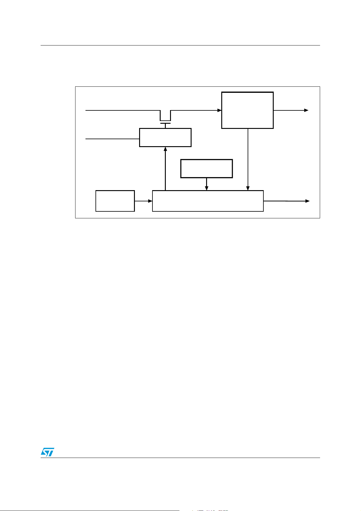
1 Block diagram
Figure 1. Block diagram
V
EN
IN
Thermal
sense
Driver
UVLO
Fault blanking/reporting
driver control unit
Current
sense
V
OUT
Fault
Doc ID 13793 Rev 4 7/34
Pin settings STMPS2141, STMPS2151, STMPS2161, STMPS2171
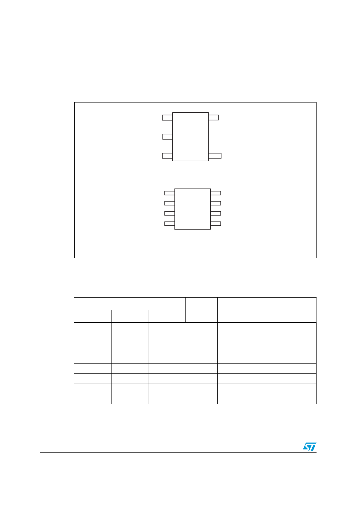
2 Pin settings
2.1 Pin connections
Figure 2. SOT23-5L, SO-8 and MSOP8 pin connections
OUT
GND
FAULT
GND
EN_N
2.2 Pin description
Table 2. Pin description
IN
IN
SO-8 / MSOP8
1
2
3
SOT23-5L
1
2
3
4
5
4
8
7
6
5
IN
EN
OUT
OUT
OUT
FAULT
Pin number
Name Function
SO8 MSOP8 SOT23-5L
1 1 2 GND Ground
2 2 5 IN 2.7 V - 5.5 V input
3 3 - IN 2.7 V - 5.5 V input
4 4 4 EN Enable for power switch
5 5 3 FAULT Open drain FAULT indicator, active low
6 6 1 OUT Output of power switch
7 7 - OUT Output of power switch
8 8 - OUT Output of power switch
8/34 Doc ID 13793 Rev 4
STMPS2141, STMPS2151, STMPS2161, STMPS2171 Functional description
3 Functional description
3.1 Fault blanking
The STMPS devices feature a 10 ms fault blanking. Fault blanking allows current-limit faults,
including momentary short-circuit faults that occur when hot-swapping a capacitive load,
and also ensures that no fault is issued during power-up. When a load transient causes the
device to enter current limit, an internal counter starts. If the load fault persists beyond the
10 ms fault-blanking timeout, the FAULT output asserts “low”. Load-transient faults less than
10 ms (typ.) do not cause a FAULT output assertion. Only current-limit faults are blanked.
Die over-temperature faults and input voltage drops below the UVLO threshold cause an
immediate fault output.
3.2 Overcurrent/over-temperature protection
In overcurrent or short-circuit condition, the switch limits the current at a value of about
120% of the rated current. If the temperature of the die goes above the limit value, the switch
turns off.
3.3 FAULT conditions
In power switch applications, 4 types of FAULT conditions are common. These fault
conditions and the response of the STMPS21x1 power switches are described in the
following Ta bl e 3 .
Table 3. FAULT conditions
Fault Condition STMPS21x1 action
Output shorted to GND via resistance
Short circuit
Over-current
Overheating
Undervoltage
path of < 1 Ω, causing a rapid current
surge.
Output connected to a load that sinks
current above threshold.
Temperature of junction exceeds 135°C
due to any reason.
Input voltage drops below the UVLO
treshold.
Reduces output voltage to reduce the
current. Asserts FAULT pin after a
blanking period
Reduces output voltage to reduce the
current. Asserts FAULT pin after a
blanking period.
Turn OFF output until temperature falls
below 125°C. Asserts FAULT pin
immediately.
Turn OFF output until input voltage rises
above the UVLO treshold plus hysteresis.
Asserts FAULT pin immediately.
Doc ID 13793 Rev 4 9/34

Functional description STMPS2141, STMPS2151, STMPS2161, STMPS2171
3.4 Reversed current blocking
When the switch is OFF (disabled through the EN pin), or when the STMPS device is un-
powered (V
reverse current will flow into the device when V
Note: In the case where the switch is ON, and a voltage higher than V
a reverse current occurs. This operating condition is not allowed.
= 0 V) the switch behaves as an Hi-Z at the output pin, ensuring that no
CC
< Vo .
i
is applied to the OUT pin,
IN
3.5 UVLO
When the input voltage drops below critical values, the power switch turns off to prevent
improper operation due to low voltage.
10/34 Doc ID 13793 Rev 4
STMPS2141, STMPS2151, STMPS2161, STMPS2171 Ambient temperature
4 Ambient temperature
In Enable operating mode, an amount of power is dissipated as heat in the power switch due
to the on-resistance. The power dissipation is: P = I
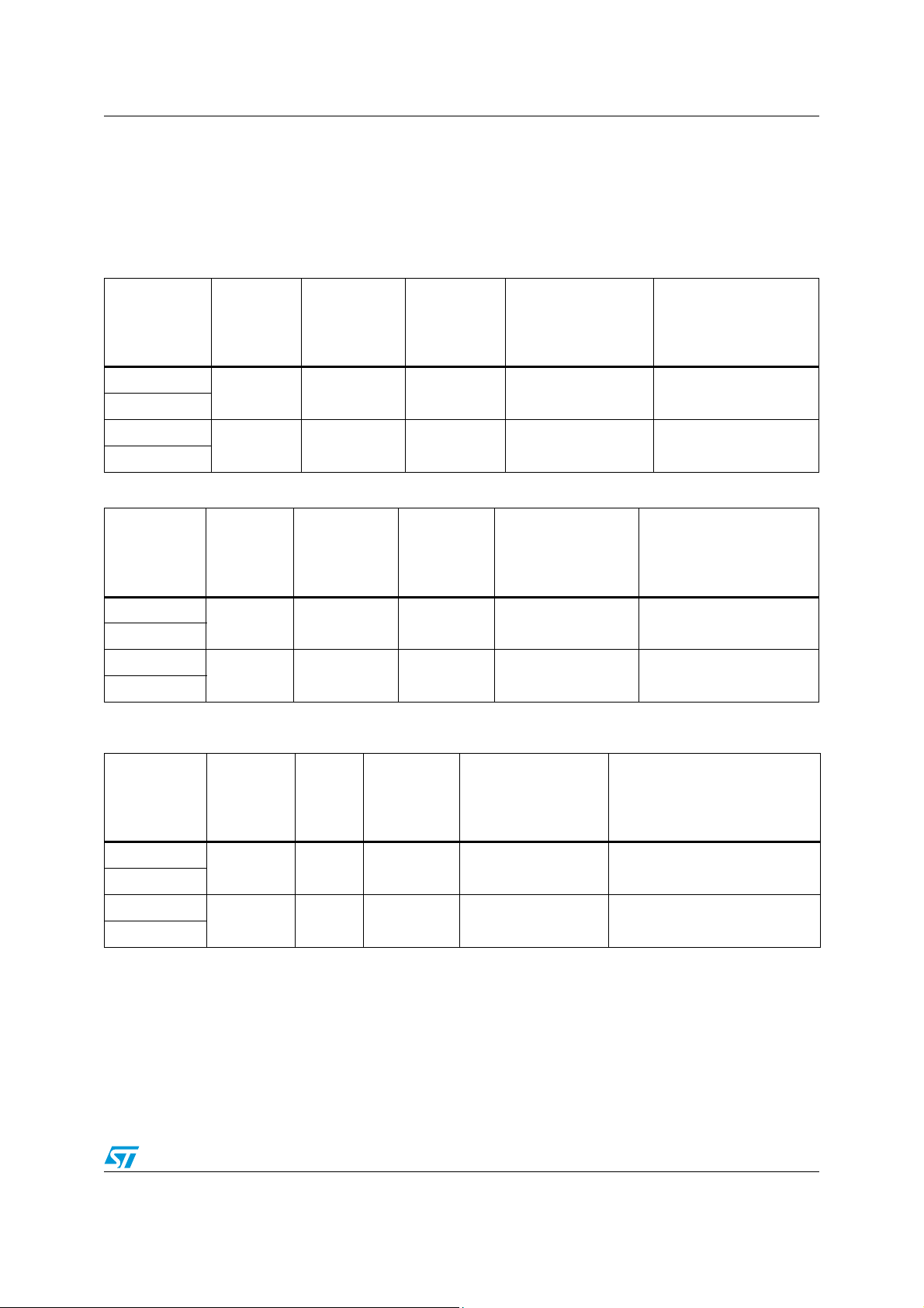
Table 4. SOT23-5L (160 °C/W)
Part number Max current
STMPS2141
STMPS2151
STMPS2161
STMPS2171
Table 5. MSOP8 (220 °C/W)
Part number
STMPS2141
STMPS2151
Max R
0.50 A 130 mΩ 32.5 mW 6.2 118.8
1.00 A 130 mΩ 130.0 mW 24.8 100.2
Max
current
Max R
at 5 V
0.50 A 130 mΩ 32.5 mW 7.2 117.8
5V
ON
ON
at
Power
dissipation
Power
dissipation
2
R.
Temperature
difference
(junction and
ambient)
Temperature
difference
(junction and
ambient)
Maximum ambient
temperature
(at junction
temperature 125 °C)
Maximum ambient
temperature
(at junction temperature
125 °C)
STMPS2161
1.00 A 130 mΩ 130.0 mW 28.6 96.4
STMPS2171
Table 6. SO-8 (160 °C/W)
Part number Max current
STMPS2141
0.50 A 130 mΩ 32.5 mΩ 5.2 124.8
STMPS2151
STMPS2161
1.00 A 130 mΩ 130.0 mΩ 20.8 104.2
STMPS2171
Max R
at 5 V
ON
Power
dissipation
Temperature
difference (junction
and ambient)
Maximum ambient
temperature
(at junction temperature
125 °C)
Doc ID 13793 Rev 4 11/34
 Loading...