

STM8AF6x26/4x/66/68
LQFP48 7x7
LQFP32 7x7
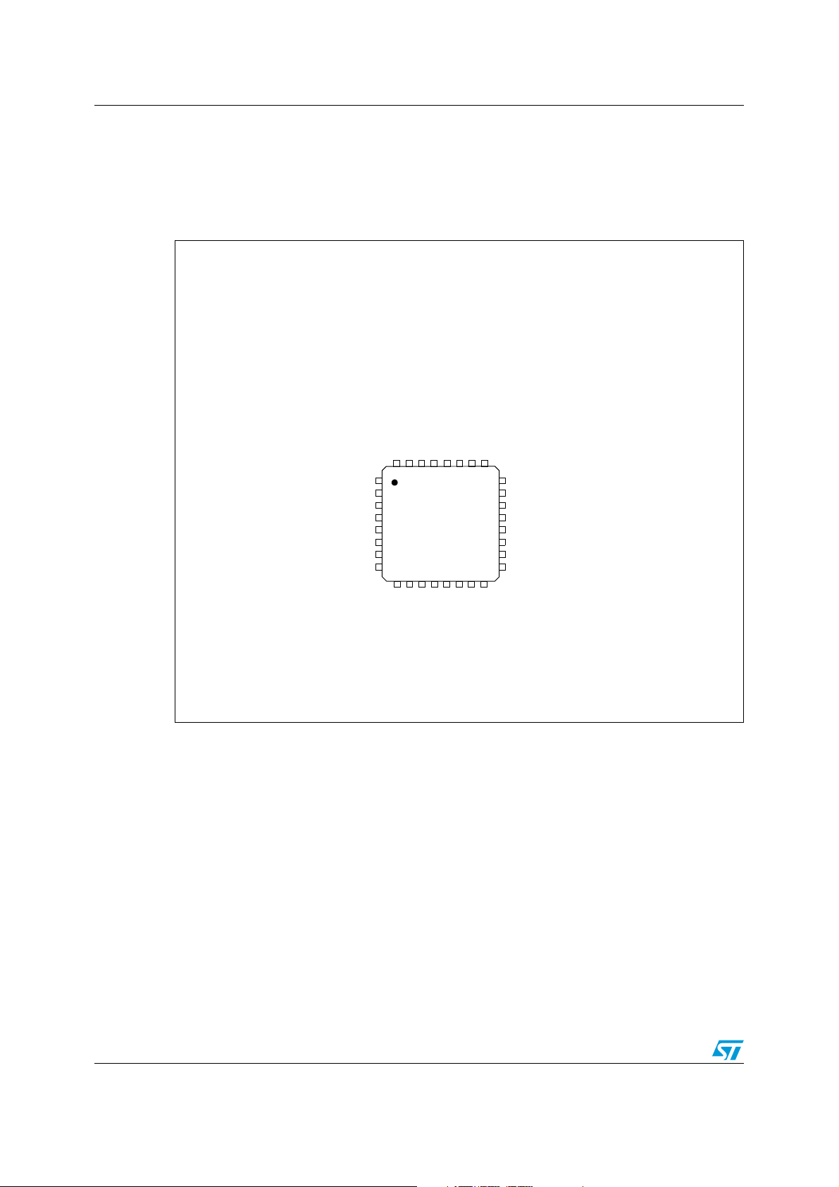
VFQFPN32 5x5
Automotive 8-bit MCU, with up to 32 Kbytes Flash, data EEPROM,
10-bit ADC, timers, LIN, SPI, I2C, 3 to 5.5 V
Datasheet − production data
Features
■ Core
–Max f
– Advanced STM8A core with Harvard
architecture and 3-stage pipeline
– Average 1.6 cycles/instruction resulting in
10 MIPS at 16 MHz f
standard benchmark
■ Memories
– Flash Program memory: 16 to 32 Kbytes
Flash; data retention 20 years at 55 °C
after 1 kcycle
– Data memory: 0.5 to 1 Kbyte true data
EEPROM; endurance 300 kcycles
– RAM: 1 to 2 Kbytes
■ Clock management
– Low-power crystal resonator oscillator with
external clock input
– Internal, user-trimmable 16 MHz RC and
low-power 128 kHz RC oscillators
– Clock security system with clock monitor
■ Reset and supply management
– Wait/auto-wakeup/Halt low-power modes
with user definable clock gating
– Low consumption power-on and power-
down reset
■ Interrupt management
– Nested interrupt controller with 32 vectors
– Up to 34 external interrupts on 5 vectors
■ Timers
– Up to 2 general purpose 16-bit PWM timers
with up to 3 CAPCOM channels each (IC,
OC or PWM)
– Advanced control timer: 16-bit, 4 CAPCOM
channels, 3 complementary outputs, dead-
time insertion and flexible synchronization
– 8-bit AR basic timer with 8-bit prescaler
– Auto-wakeup timer
CPU
: 16 MHz
for industry
CPU
– Window and independent watchdog timers
■ Communication interfaces
–LINUART
– LIN 2.1 compliant, master/slave modes
with automatic resynchronization
– SPI interface up to 10 Mbit/s or f
2
–I
C interface up to 400 Kbit/s
■ Analog-to-digital converter (ADC)
MASTER
– 10-bit accuracy, 2LSB TUE accuracy, 2LSB
TUE linearity ADC and up to 10 multiplexed
channels with individual data buffer
– Analog watchdog, scan and continuous
sampling mode
■ I/Os
– Up to 38 user pins including 10 HS I/Os
– Highly robust I/O design, immune against
current injection
■ Operating temperature up to 150 °C
■ Qualification conforms to AEC-Q100 rev G
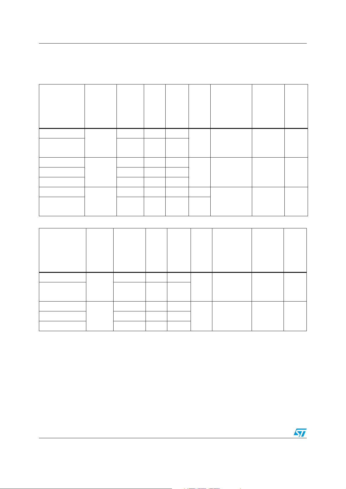
Table 1. Device summary
Part numbers: STM8AF622x/4x STM8AF6266/68
STM8AF6268, STM8AF6248, STM8AF6266, STM8AF6246,
STM8AF6226
Part numbers: STM8AF612x/4x
STM8AF6168, STM8AF6148, STM8AF6166, STM8AF6146,
STM8AF6126
In the order code, ‘F’ applies to devices with Flash program
1.
memory and data EEPROM while ‘H’ refers to devices with
Flash program memory only. ‘F’ is replaced by ‘P’ for devices
with FASTROM (see Tables 2 and 3, and Figure 47).
2. Not recommended for new design.
(1)
(2)
STM8AF6166/68
(2)
/2
July 2012 Doc ID 14952 Rev 6 1/89
This is information on a product in full production.
www.st.com
1

Contents STM8AF61xx, STM8AF62xx
Contents
1 Introduction . . . . . . . . . . . . . . . . . . . . . . . . . . . . . . . . . . . . . . . . . . . . . . . . 8
2 Description . . . . . . . . . . . . . . . . . . . . . . . . . . . . . . . . . . . . . . . . . . . . . . . . . 9
3 Product line-up . . . . . . . . . . . . . . . . . . . . . . . . . . . . . . . . . . . . . . . . . . . . 10
4 Block diagram . . . . . . . . . . . . . . . . . . . . . . . . . . . . . . . . . . . . . . . . . . . . . 11
5 Product overview . . . . . . . . . . . . . . . . . . . . . . . . . . . . . . . . . . . . . . . . . . 12
5.1 STM8A central processing unit (CPU) . . . . . . . . . . . . . . . . . . . . . . . . . . . 12
5.1.1 Architecture and registers . . . . . . . . . . . . . . . . . . . . . . . . . . . . . . . . . . . 12
5.1.2 Addressing . . . . . . . . . . . . . . . . . . . . . . . . . . . . . . . . . . . . . . . . . . . . . . . 12
5.1.3 Instruction set . . . . . . . . . . . . . . . . . . . . . . . . . . . . . . . . . . . . . . . . . . . . 12
5.2 Single wire interface module (SWIM) and debug module (DM) . . . . . . . . 13
5.2.1 SWIM . . . . . . . . . . . . . . . . . . . . . . . . . . . . . . . . . . . . . . . . . . . . . . . . . . . 13
5.2.2 Debug module . . . . . . . . . . . . . . . . . . . . . . . . . . . . . . . . . . . . . . . . . . . . 13
5.3 Interrupt controller . . . . . . . . . . . . . . . . . . . . . . . . . . . . . . . . . . . . . . . . . . 13
5.4 Flash program and data EEPROM . . . . . . . . . . . . . . . . . . . . . . . . . . . . . . 13
5.4.1 Architecture . . . . . . . . . . . . . . . . . . . . . . . . . . . . . . . . . . . . . . . . . . . . . . 13
5.4.2 Write protection (WP) . . . . . . . . . . . . . . . . . . . . . . . . . . . . . . . . . . . . . . 14
5.4.3 Protection of user boot code (UBC) . . . . . . . . . . . . . . . . . . . . . . . . . . . . 14
5.4.4 Read-out protection (ROP) . . . . . . . . . . . . . . . . . . . . . . . . . . . . . . . . . . 14
5.5 Clock controller . . . . . . . . . . . . . . . . . . . . . . . . . . . . . . . . . . . . . . . . . . . . . 15
5.5.1 Features . . . . . . . . . . . . . . . . . . . . . . . . . . . . . . . . . . . . . . . . . . . . . . . . . 15
5.5.2 16 MHz high-speed internal RC oscillator (HSI) . . . . . . . . . . . . . . . . . . 15
5.5.3 128 kHz low-speed internal RC oscillator (LSI) . . . . . . . . . . . . . . . . . . . 16
5.5.4 16 MHz high-speed external crystal oscillator (HSE) . . . . . . . . . . . . . . 16
5.5.5 External clock input . . . . . . . . . . . . . . . . . . . . . . . . . . . . . . . . . . . . . . . . 16
5.5.6 Clock security system (CSS) . . . . . . . . . . . . . . . . . . . . . . . . . . . . . . . . . 16
5.6 Low-power operating modes . . . . . . . . . . . . . . . . . . . . . . . . . . . . . . . . . . 17
5.7 Timers . . . . . . . . . . . . . . . . . . . . . . . . . . . . . . . . . . . . . . . . . . . . . . . . . . . 17
5.7.1 Watchdog timers . . . . . . . . . . . . . . . . . . . . . . . . . . . . . . . . . . . . . . . . . . 17
5.7.2 Auto-wakeup counter . . . . . . . . . . . . . . . . . . . . . . . . . . . . . . . . . . . . . . . 18
5.7.3 Beeper . . . . . . . . . . . . . . . . . . . . . . . . . . . . . . . . . . . . . . . . . . . . . . . . . . 18
2/89 Doc ID 14952 Rev 6

STM8AF61xx, STM8AF62xx Contents
5.7.4 Advanced control and general purpose timers . . . . . . . . . . . . . . . . . . . 18
5.7.5 Basic timer . . . . . . . . . . . . . . . . . . . . . . . . . . . . . . . . . . . . . . . . . . . . . . . 19
5.8 Analog-to-digital converter (ADC) . . . . . . . . . . . . . . . . . . . . . . . . . . . . . . 20
5.9 Communication interfaces . . . . . . . . . . . . . . . . . . . . . . . . . . . . . . . . . . . . 20
5.9.1 Serial peripheral interface (SPI) . . . . . . . . . . . . . . . . . . . . . . . . . . . . . . . 21
5.9.2 Inter integrated circuit (I
5.9.3 Universal asynchronous receiver/transmitter with LIN support
(LINUART) . . . . . . . . . . . . . . . . . . . . . . . . . . . . . . . . . . . . . . . . . . . . . . . 22
2
C) interface . . . . . . . . . . . . . . . . . . . . . . . . . . . 21
5.10 Input/output specifications . . . . . . . . . . . . . . . . . . . . . . . . . . . . . . . . . . . . 23
6 Pinouts and pin description . . . . . . . . . . . . . . . . . . . . . . . . . . . . . . . . . . 24
6.1 Package pinouts . . . . . . . . . . . . . . . . . . . . . . . . . . . . . . . . . . . . . . . . . . . . 24
6.2 Alternate function remapping . . . . . . . . . . . . . . . . . . . . . . . . . . . . . . . . . . 28
7 Memory and register map . . . . . . . . . . . . . . . . . . . . . . . . . . . . . . . . . . . 29
7.1 Memory map . . . . . . . . . . . . . . . . . . . . . . . . . . . . . . . . . . . . . . . . . . . . . . 29
7.2 Register map . . . . . . . . . . . . . . . . . . . . . . . . . . . . . . . . . . . . . . . . . . . . . . 30
8 Interrupt table . . . . . . . . . . . . . . . . . . . . . . . . . . . . . . . . . . . . . . . . . . . . . 40
9 Option bytes . . . . . . . . . . . . . . . . . . . . . . . . . . . . . . . . . . . . . . . . . . . . . . 41
10 Electrical characteristics . . . . . . . . . . . . . . . . . . . . . . . . . . . . . . . . . . . . 46
10.1 Parameter conditions . . . . . . . . . . . . . . . . . . . . . . . . . . . . . . . . . . . . . . . . 46
10.1.1 Minimum and maximum values . . . . . . . . . . . . . . . . . . . . . . . . . . . . . . . 46
10.1.2 Typical values . . . . . . . . . . . . . . . . . . . . . . . . . . . . . . . . . . . . . . . . . . . . . 46
10.1.3 Typical curves . . . . . . . . . . . . . . . . . . . . . . . . . . . . . . . . . . . . . . . . . . . . 46
10.1.4 Loading capacitor . . . . . . . . . . . . . . . . . . . . . . . . . . . . . . . . . . . . . . . . . 46
10.1.5 Pin input voltage . . . . . . . . . . . . . . . . . . . . . . . . . . . . . . . . . . . . . . . . . . 47
10.2 Absolute maximum ratings . . . . . . . . . . . . . . . . . . . . . . . . . . . . . . . . . . . . 47
10.3 Operating conditions . . . . . . . . . . . . . . . . . . . . . . . . . . . . . . . . . . . . . . . . 49
10.3.1 VCAP external capacitor . . . . . . . . . . . . . . . . . . . . . . . . . . . . . . . . . . . . 51
10.3.2 Supply current characteristics . . . . . . . . . . . . . . . . . . . . . . . . . . . . . . . . 51
10.3.3 External clock sources and timing characteristics . . . . . . . . . . . . . . . . . 54
10.3.4 Internal clock sources and timing characteristics . . . . . . . . . . . . . . . . . 56
10.3.5 Memory characteristics . . . . . . . . . . . . . . . . . . . . . . . . . . . . . . . . . . . . . 58
10.3.6 I/O port pin characteristics . . . . . . . . . . . . . . . . . . . . . . . . . . . . . . . . . . . 59
Doc ID 14952 Rev 6 3/89

Contents STM8AF61xx, STM8AF62xx
10.3.7 Reset pin characteristics . . . . . . . . . . . . . . . . . . . . . . . . . . . . . . . . . . . . 63
10.3.8 TIM 1, 2, 3, and 4 timer specifications . . . . . . . . . . . . . . . . . . . . . . . . . . 65
10.3.9 SPI serial peripheral interface . . . . . . . . . . . . . . . . . . . . . . . . . . . . . . . . 65
10.3.10 I
10.3.11 10-bit ADC characteristics . . . . . . . . . . . . . . . . . . . . . . . . . . . . . . . . . . . 69
10.3.12 EMC characteristics . . . . . . . . . . . . . . . . . . . . . . . . . . . . . . . . . . . . . . . . 71
2
C interface characteristics . . . . . . . . . . . . . . . . . . . . . . . . . . . . . . . . . . 68
10.4 Thermal characteristics . . . . . . . . . . . . . . . . . . . . . . . . . . . . . . . . . . . . . . 73
10.4.1 Reference document . . . . . . . . . . . . . . . . . . . . . . . . . . . . . . . . . . . . . . . 74
10.4.2 Selecting the product temperature range . . . . . . . . . . . . . . . . . . . . . . . . 74
11 Package characteristics . . . . . . . . . . . . . . . . . . . . . . . . . . . . . . . . . . . . . 75
11.1 Package mechanical data . . . . . . . . . . . . . . . . . . . . . . . . . . . . . . . . . . . . 76
12 Ordering information . . . . . . . . . . . . . . . . . . . . . . . . . . . . . . . . . . . . . . . 81
13 STM8 development tools . . . . . . . . . . . . . . . . . . . . . . . . . . . . . . . . . . . . 82
13.1 Emulation and in-circuit debugging tools . . . . . . . . . . . . . . . . . . . . . . . . . 82
13.1.1 STice key features . . . . . . . . . . . . . . . . . . . . . . . . . . . . . . . . . . . . . . . . . 82
13.2 Software tools . . . . . . . . . . . . . . . . . . . . . . . . . . . . . . . . . . . . . . . . . . . . . . 83
13.2.1 STM8 toolset . . . . . . . . . . . . . . . . . . . . . . . . . . . . . . . . . . . . . . . . . . . . . 83
13.2.2 C and assembly toolchains . . . . . . . . . . . . . . . . . . . . . . . . . . . . . . . . . . 83
13.3 Programming tools . . . . . . . . . . . . . . . . . . . . . . . . . . . . . . . . . . . . . . . . . . 84
14 Revision history . . . . . . . . . . . . . . . . . . . . . . . . . . . . . . . . . . . . . . . . . . . 85
4/89 Doc ID 14952 Rev 6

STM8AF61xx, STM8AF62xx List of tables
List of tables
Table 1. Device summary . . . . . . . . . . . . . . . . . . . . . . . . . . . . . . . . . . . . . . . . . . . . . . . . . . . . . . . . . . 1
Table 2. STM8AF62xx product line-up . . . . . . . . . . . . . . . . . . . . . . . . . . . . . . . . . . . . . . . . . . . . . . . 10
Table 3. STM8AF/H61xx product line-up . . . . . . . . . . . . . . . . . . . . . . . . . . . . . . . . . . . . . . . . . . . . . 10
Table 4. Peripheral clock gating bit assignments in CLK_PCKENR1/2 registers . . . . . . . . . . . . . . . 16
Table 5. Advanced control and general purpose timers . . . . . . . . . . . . . . . . . . . . . . . . . . . . . . . . . . 18
Table 6. TIM4 . . . . . . . . . . . . . . . . . . . . . . . . . . . . . . . . . . . . . . . . . . . . . . . . . . . . . . . . . . . . . . . . . . 19
Table 7. ADC naming . . . . . . . . . . . . . . . . . . . . . . . . . . . . . . . . . . . . . . . . . . . . . . . . . . . . . . . . . . . . 20
Table 8. Communication peripheral naming correspondence . . . . . . . . . . . . . . . . . . . . . . . . . . . . . 20
Table 9. Legend/abbreviation . . . . . . . . . . . . . . . . . . . . . . . . . . . . . . . . . . . . . . . . . . . . . . . . . . . . . . 25
Table 10. STM8AF61xx/62xx (32 Kbytes) microcontroller pin description . . . . . . . . . . . . . . . . . . . . . 26
Table 11. Memory model for the devices covered in this datasheet. . . . . . . . . . . . . . . . . . . . . . . . . . 29
Table 12. I/O port hardware register map . . . . . . . . . . . . . . . . . . . . . . . . . . . . . . . . . . . . . . . . . . . . . . 30
Table 13. General hardware register map . . . . . . . . . . . . . . . . . . . . . . . . . . . . . . . . . . . . . . . . . . . . . 31
Table 14. CPU/SWIM/debug module/interrupt controller registers . . . . . . . . . . . . . . . . . . . . . . . . . . . 38
Table 15. Temporary memory unprotection registers. . . . . . . . . . . . . . . . . . . . . . . . . . . . . . . . . . . . . 39
Table 16. STM8A interrupt table . . . . . . . . . . . . . . . . . . . . . . . . . . . . . . . . . . . . . . . . . . . . . . . . . . . . . 40
Table 17. Option bytes . . . . . . . . . . . . . . . . . . . . . . . . . . . . . . . . . . . . . . . . . . . . . . . . . . . . . . . . . . . . 41
Table 18. Option byte description . . . . . . . . . . . . . . . . . . . . . . . . . . . . . . . . . . . . . . . . . . . . . . . . . . . . 43
Table 19. Voltage characteristics . . . . . . . . . . . . . . . . . . . . . . . . . . . . . . . . . . . . . . . . . . . . . . . . . . . . 47
Table 20. Current characteristics . . . . . . . . . . . . . . . . . . . . . . . . . . . . . . . . . . . . . . . . . . . . . . . . . . . . 48
Table 21. Thermal characteristics. . . . . . . . . . . . . . . . . . . . . . . . . . . . . . . . . . . . . . . . . . . . . . . . . . . . 48
Table 22. Operating lifetime . . . . . . . . . . . . . . . . . . . . . . . . . . . . . . . . . . . . . . . . . . . . . . . . . . . . . . . . 48
Table 23. General operating conditions . . . . . . . . . . . . . . . . . . . . . . . . . . . . . . . . . . . . . . . . . . . . . . . 49
Table 24. Operating conditions at power-up/power-down . . . . . . . . . . . . . . . . . . . . . . . . . . . . . . . . . 50
Table 25. Total current consumption in Run, Wait and Slow mode.
General conditions for V
Table 26. Total current consumption in Halt and Active-halt modes.
General conditions for V
Table 27. Oscillator current consumption . . . . . . . . . . . . . . . . . . . . . . . . . . . . . . . . . . . . . . . . . . . . . . 52
Table 28. Programming current consumption. . . . . . . . . . . . . . . . . . . . . . . . . . . . . . . . . . . . . . . . . . . 53
Table 29. Typical peripheral current consumption V
Table 30. HSE user external clock characteristics . . . . . . . . . . . . . . . . . . . . . . . . . . . . . . . . . . . . . . . 54
Table 31. HSE oscillator characteristics . . . . . . . . . . . . . . . . . . . . . . . . . . . . . . . . . . . . . . . . . . . . . . . 55
Table 32. HSI oscillator characteristics. . . . . . . . . . . . . . . . . . . . . . . . . . . . . . . . . . . . . . . . . . . . . . . . 56
Table 33. LSI oscillator characteristics . . . . . . . . . . . . . . . . . . . . . . . . . . . . . . . . . . . . . . . . . . . . . . . . 57
Table 34. Flash program memory/data EEPROM memory . . . . . . . . . . . . . . . . . . . . . . . . . . . . . . . . 58
Table 35. Flash program memory. . . . . . . . . . . . . . . . . . . . . . . . . . . . . . . . . . . . . . . . . . . . . . . . . . . . 58
Table 36. Data memory . . . . . . . . . . . . . . . . . . . . . . . . . . . . . . . . . . . . . . . . . . . . . . . . . . . . . . . . . . . 58
Table 37. I/O static characteristics . . . . . . . . . . . . . . . . . . . . . . . . . . . . . . . . . . . . . . . . . . . . . . . . . . . 59
Table 38. NRST pin characteristics . . . . . . . . . . . . . . . . . . . . . . . . . . . . . . . . . . . . . . . . . . . . . . . . . . 63
Table 39. TIM 1, 2, 3, and 4 electrical specifications . . . . . . . . . . . . . . . . . . . . . . . . . . . . . . . . . . . . . 65
Table 40. SPI characteristics . . . . . . . . . . . . . . . . . . . . . . . . . . . . . . . . . . . . . . . . . . . . . . . . . . . . . . . 65
Table 41. I
2
C characteristics. . . . . . . . . . . . . . . . . . . . . . . . . . . . . . . . . . . . . . . . . . . . . . . . . . . . . . . . 68
Table 42. ADC characteristics . . . . . . . . . . . . . . . . . . . . . . . . . . . . . . . . . . . . . . . . . . . . . . . . . . . . . . 69
Table 43. ADC accuracy for V
DDA
Table 44. EMS data . . . . . . . . . . . . . . . . . . . . . . . . . . . . . . . . . . . . . . . . . . . . . . . . . . . . . . . . . . . . . . 71
Table 45. EMI data . . . . . . . . . . . . . . . . . . . . . . . . . . . . . . . . . . . . . . . . . . . . . . . . . . . . . . . . . . . . . . . 72
Table 46. ESD absolute maximum ratings . . . . . . . . . . . . . . . . . . . . . . . . . . . . . . . . . . . . . . . . . . . . . 72
apply, TA = -40 to 150 °C . . . . . . . . . . . . . . . . . . . . . . . . . . . . 51
DD
apply, TA = -40 to 55 °C . . . . . . . . . . . . . . . . . . . . . . . . . . . . . 52
DD
= 5.0 V . . . . . . . . . . . . . . . . . . . . . . . . . . . . . 53
DD
= 5 V. . . . . . . . . . . . . . . . . . . . . . . . . . . . . . . . . . . . . . . . . . . . . . . 70
Doc ID 14952 Rev 6 5/89

List of tables STM8AF61xx, STM8AF62xx
Table 47. Electrical sensitivities . . . . . . . . . . . . . . . . . . . . . . . . . . . . . . . . . . . . . . . . . . . . . . . . . . . . . 73
Table 48. Thermal characteristics. . . . . . . . . . . . . . . . . . . . . . . . . . . . . . . . . . . . . . . . . . . . . . . . . . . . 74
Table 49. VFQFPN 32-lead very thin fine pitch quad flat no-lead package
mechanical data. . . . . . . . . . . . . . . . . . . . . . . . . . . . . . . . . . . . . . . . . . . . . . . . . . . . . . . . . 76
Table 50. LQFP 48-pin low profile quad flat package mechanical data . . . . . . . . . . . . . . . . . . . . . . . 77
Table 51. LQFP 32-pin low profile quad flat package mechanical data . . . . . . . . . . . . . . . . . . . . . . . 79
Table 52. Document revision history . . . . . . . . . . . . . . . . . . . . . . . . . . . . . . . . . . . . . . . . . . . . . . . . . 85
6/89 Doc ID 14952 Rev 6

STM8AF61xx, STM8AF62xx List of figures
List of figures
Figure 1. STM8A block diagram . . . . . . . . . . . . . . . . . . . . . . . . . . . . . . . . . . . . . . . . . . . . . . . . . . . . 11
Figure 2. Flash memory organization of STM8A products. . . . . . . . . . . . . . . . . . . . . . . . . . . . . . . . . 14
Figure 3. VFQFPN/LQFP 32-pin pinout . . . . . . . . . . . . . . . . . . . . . . . . . . . . . . . . . . . . . . . . . . . . . . . 24
Figure 4. LQFP 48-pin pinout. . . . . . . . . . . . . . . . . . . . . . . . . . . . . . . . . . . . . . . . . . . . . . . . . . . . . . . 25
Figure 5. Register and memory map of STM8A products . . . . . . . . . . . . . . . . . . . . . . . . . . . . . . . . . 29
Figure 6. Pin loading conditions . . . . . . . . . . . . . . . . . . . . . . . . . . . . . . . . . . . . . . . . . . . . . . . . . . . . . 46
Figure 7. Pin input voltage . . . . . . . . . . . . . . . . . . . . . . . . . . . . . . . . . . . . . . . . . . . . . . . . . . . . . . . . . 47
Figure 8. f
CPUmax
Figure 9. External capacitor C
Figure 10. Typ. I
Figure 11. Typ. I
Figure 12. Typ. I
Figure 13. Typ. I
Figure 14. Typ. I
Figure 15. Typ. I
Figure 16. HSE external clock source . . . . . . . . . . . . . . . . . . . . . . . . . . . . . . . . . . . . . . . . . . . . . . . . . 55
Figure 17. HSE oscillator circuit diagram . . . . . . . . . . . . . . . . . . . . . . . . . . . . . . . . . . . . . . . . . . . . . . . 55
Figure 18. Typical HSI frequency vs V
Figure 19. Typical LSI frequency vs V
Figure 20. Typical V
Figure 21. Typical pull-up resistance R
Figure 22. Typical pull-up current I
Figure 23. Typ. V
Figure 24. Typ. V
Figure 25. Typ. V
Figure 26. Typ. V
Figure 27. Typ. V
Figure 28. Typ. V
Figure 29. Typ. V
Figure 30. Typ. V
Figure 31. Typ. V
Figure 32. Typ. V
Figure 33. Typical NRST V
Figure 34. Typical NRST pull-up resistance R
Figure 35. Typical NRST pull-up current I
Figure 36. Recommended reset pin protection . . . . . . . . . . . . . . . . . . . . . . . . . . . . . . . . . . . . . . . . . . 64
Figure 37. SPI timing diagram where slave mode and CPHA = 0 . . . . . . . . . . . . . . . . . . . . . . . . . . . . 66
Figure 38. SPI timing diagram where slave mode and CPHA = 1 . . . . . . . . . . . . . . . . . . . . . . . . . . . . 66
Figure 39. SPI timing diagram - master mode . . . . . . . . . . . . . . . . . . . . . . . . . . . . . . . . . . . . . . . . . . . 67
Figure 40. Typical application with ADC . . . . . . . . . . . . . . . . . . . . . . . . . . . . . . . . . . . . . . . . . . . . . . . 69
Figure 41. ADC accuracy characteristics. . . . . . . . . . . . . . . . . . . . . . . . . . . . . . . . . . . . . . . . . . . . . . . 70
Figure 42. VFQFPN 32-lead very thin fine pitch quad flat no-lead package (5 x 5). . . . . . . . . . . . . . . 76
Figure 43. LQFP 48-pin low profile quad flat package (7 x 7) . . . . . . . . . . . . . . . . . . . . . . . . . . . . . . . 77
Figure 44. LQFP 48-pin recommended footprint . . . . . . . . . . . . . . . . . . . . . . . . . . . . . . . . . . . . . . . . . 78
Figure 45. LQFP 32-pin low profile quad flat package (7 x 7) . . . . . . . . . . . . . . . . . . . . . . . . . . . . . . . 79
Figure 46. LQFP 32-pin recommended footprint . . . . . . . . . . . . . . . . . . . . . . . . . . . . . . . . . . . . . . . . . 80
Figure 47. Ordering information scheme
versus V
DD(RUN)HSE
DD(RUN)HSE
DD(RUN)HSI
DD(WFI)HSE
DD(WFI)HSE
DD(WFI)HSI
IL
@ VDD = 3.3 V (standard ports). . . . . . . . . . . . . . . . . . . . . . . . . . . . . . . . . . . . . . 61
OL
@ VDD = 5.0 V (standard ports). . . . . . . . . . . . . . . . . . . . . . . . . . . . . . . . . . . . . . 61
OL
@ VDD = 3.3 V (true open drain ports) . . . . . . . . . . . . . . . . . . . . . . . . . . . . . . . . 61
OL
@ VDD = 5.0 V (true open drain ports) . . . . . . . . . . . . . . . . . . . . . . . . . . . . . . . . 61
OL
@ VDD = 3.3 V (high sink ports) . . . . . . . . . . . . . . . . . . . . . . . . . . . . . . . . . . . . . 62
OL
@ VDD = 5.0 V (high sink ports) . . . . . . . . . . . . . . . . . . . . . . . . . . . . . . . . . . . . . 62
OL
- V
DD
- V
DD
- VOH @ VDD = 3.3 V (high sink ports) . . . . . . . . . . . . . . . . . . . . . . . . . . . . . . . . 62
DD
- V
DD
DD . . . . . . . . . . . . . . . . . . . . . . . . . . . . . . . . . . . . . . . . . . . . . . . . . . . . . . . . . . . . . . . . . . . . . 50
vs. VDD @f
vs. f
vs. VDD @ f
vs. VDD @ f
vs. f
vs. VDD @ f
. . . . . . . . . . . . . . . . . . . . . . . . . . . . . . . . . . . . . . . . . . . . . . . . . . . 51
EXT
@ VDD = 5.0 V, peripheral = on . . . . . . . . . . . . . . . . . . . . . . . . 53
CPU
@ VDD = 5.0 V, peripheral = on . . . . . . . . . . . . . . . . . . . . . . . . . 54
CPU
= 16 MHz, peripheral = on . . . . . . . . . . . . . . . . . . . . . . . 53
CPU
= 16 MHz, peripheral = off . . . . . . . . . . . . . . . . . . . . . . . 54
CPU
= 16 MHz, peripheral = on . . . . . . . . . . . . . . . . . . . . . . . 54
CPU
= 16 MHz, peripheral = off . . . . . . . . . . . . . . . . . . . . . . . 54
CPU
. . . . . . . . . . . . . . . . . . . . . . . . . . . . . . . . . . . . . . . . . . . . . . . 57
DD
. . . . . . . . . . . . . . . . . . . . . . . . . . . . . . . . . . . . . . . . . . . . . . . 57
DD
and VIH vs VDD @ four temperatures . . . . . . . . . . . . . . . . . . . . . . . . . . . . . . . . 60
vs VDD @ four temperatures . . . . . . . . . . . . . . . . . . . . . . . 60
PU
vs VDD @ four temperatures . . . . . . . . . . . . . . . . . . . . . . . . . . . 61
pu
@ VDD = 3.3 V (standard ports). . . . . . . . . . . . . . . . . . . . . . . . . . . . . . . . . 62
OH
@ VDD = 5.0 V (standard ports). . . . . . . . . . . . . . . . . . . . . . . . . . . . . . . . . 62
OH
@ VDD = 5.0 V (high sink ports) . . . . . . . . . . . . . . . . . . . . . . . . . . . . . . . . 62
OH
and VIH vs VDD @ four temperatures . . . . . . . . . . . . . . . . . . . . . . . . . . 63
IL
pu
(1)
vs VDD. . . . . . . . . . . . . . . . . . . . . . . . . . . . . . . . . . . 64
PU
vs VDD . . . . . . . . . . . . . . . . . . . . . . . . . . . . . . . . . . . . . . 64
. . . . . . . . . . . . . . . . . . . . . . . . . . . . . . . . . . . . . . . . . . . . . 81
Doc ID 14952 Rev 6 7/89

Introduction STM8AF61xx, STM8AF62xx
1 Introduction
This datasheet refers to the STM8AF61xx (STM8AF612x, STM8AF614x, STM8AF6166,
and STM8AF6168) and STM8AF62xx products with 16 to 32 Kbytes of Flash program
memory.
In the order code, the letter ‘F’ refers to product versions with data EEPROM and ‘H’ refers
to product versions without data EEPROM. The identifiers ‘F’ and ‘H’ do not coexist in a
given order code.
The datasheet contains the description of family features, pinout, electrical characteristics,
mechanical data and ordering information.
● For complete information on the STM8A microcontroller memory, registers and
peripherals, please refer to STM8S and STM8A microcontroller families reference
manual (RM0016).
● For information on programming, erasing and protection of the internal Flash memory
please refer to the STM8 Flash programming manual (PM0051).
● For information on the debug and SWIM (single wire interface module) refer to the
STM8 SWIM communication protocol and debug module user manual (UM0470).
● For information on the STM8 core, please refer to the STM8 CPU programming manual
(PM0044).
8/89 Doc ID 14952 Rev 6

STM8AF61xx, STM8AF62xx Description
2 Description
The STM8AF61xx and STM8AF62xx automotive 8-bit microcontrollers offer from 16 to 32
Kbytes of Flash program memory and integrated true data EEPROM. They are referred to
as medium density STM8A devices in the STM8S and STM8A microcontroller families
reference manual (RM0016).
All devices of the STM8A product line provide the following benefits: reduced system cost,
performance and robustness, short development cycles, and product longevity.
The system cost is reduced thanks to an integrated true data EEPROM for up to 300 k
write/erase cycles and a high system integration level with internal clock oscillators,
watchdog, and brown-out reset.
Device performance is ensured by a clock frequency of up to 16 MHz CPU and enhanced
characteristics which include robust I/O, independent watchdogs (with a separate clock
source), and a clock security system.
Short development cycles are guaranteed due to application scalability across a common
family product architecture with compatible pinout, memory map and and modular
peripherals. Full documentation is offered with a wide choice of development tools.
Product longevity is ensured in the STM8A family thanks to their advanced core which is
made in a state-of-the art technology for automotive applications with 3.3 V to 5 V operating
supply.
All STM8A and ST7 microcontrollers are supported by the same tools including
STVD/STVP development environment, the STice emulator and a low-cost, third party incircuit debugging tool.
Doc ID 14952 Rev 6 9/89
Product line-up STM8AF61xx, STM8AF62xx
3 Product line-up
²
Table 2. STM8AF62xx product line-up
Medium
Order code Package
density
Flash
program
memory
(bytes)
RAM
(bytes)
Data EE
(bytes)
10-bit
A/D ch.
Timers
(IC/OC/PWM)
Serial
interfaces
I/0
wakeup
pins
STM8AF/P6268
32 K 2 K 1 K
LQFP48
STM8AF/P6248 16 K 2 K 0.5 K
STM8AF/P6266
(7x7)
32 K 2 K 1 K
LQFP32
(7x7)
STM8AF/P6226 8 K 2 K 384
STM8AF/P6266
32 K 2 K 1 K 7 1x8-bit: TIM4
VFQFPN32
STM8AF/P6246 16 K 2 K 0.5 K
²
Table 3. STM8AF/H61xx product line-up
(1)
Medium
density
Order code Package
Flash
program
RAM
(bytes)
Data EE
(bytes)
memory
(bytes)
STM8AF/H/P6168
32 K 2 K 1 K
LQFP48
STM8AF/H/P6148 16 K 1 K 0.5 K
STM8AF/H/P6166
(7x7)
32 K 2 K 1 K
LQFP32
(7x7)
STM8AF/H/P6126 8 K 512 384
1. These devices are not recommended for new design.
10
7
10-bit
A/D ch.
10
7
1x8-bit: TIM4
3x16-bit: TIM1,
TIM2, TIM3
(9/9/9)
1x8-bit: TIM4
3x16-bit: TIM1,
TIM2, TIM3
(8/8/8)
3x16-bit: TIM1,
TIM2, TIM3
(8/8/8)
Timers
(IC/OC/PWM)
1x8-bit: TIM4
3x16-bit: TIM1,
TIM2, TIM3
(9/9/9)
1x8-bit: TIM4
3x16-bit: TIM1,
TIM2, TIM3
(8/8/8)
LIN(UART),
SPI, I²C
LIN(UART),
SPI, I²C
LIN(UART),
SPI, I²C
Serial
interfaces
LIN(UART),
SPI, I²C
LIN(UART),
SPI, I²C
38/35
25/23STM8AF/P6246 16 K 2 K 0.5 K
25/23
I/0
wakeup
pins
38/35
25/23STM8AF/H/P6146 16 K 1 K 0.5 K
10/89 Doc ID 14952 Rev 6
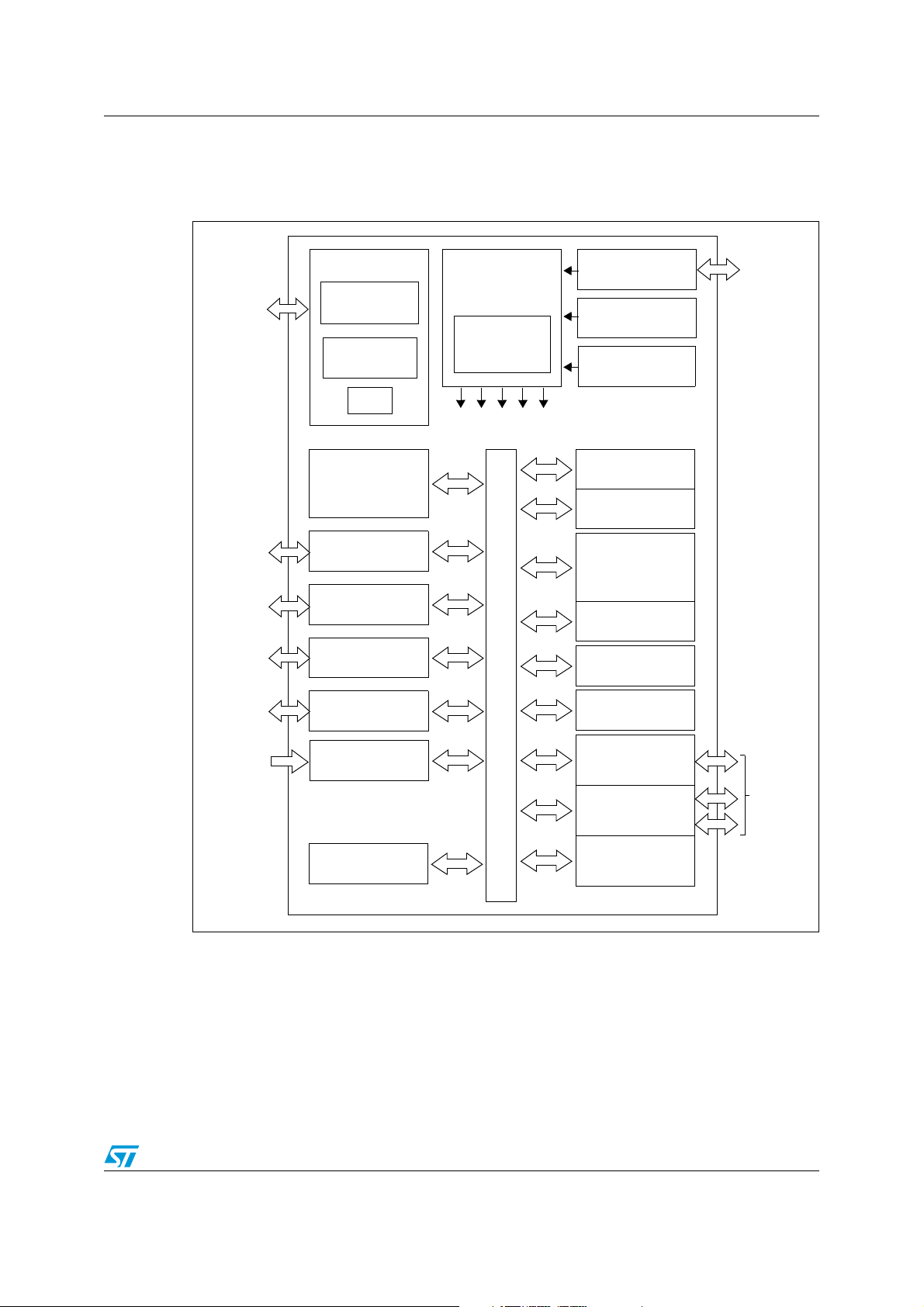
STM8AF61xx, STM8AF62xx Block diagram
XTAL 1 - 16 MHz
RC int. 16 MHz
RC int. 128 kHz
STM8A CORE
Debug/SWIM
I
2
C
SPI
LINUART
16-bit general purpose
AWU tim er
Reset block
Reset
Clock controller
Detector
Clock to peripherals and core
10 Mbit/s
16 channels
Window WDG
IWDG
Up to 32 Kbytes
Up to 1 Kbytes
Up to 2 Kbytes
Boot ROM
10-bit ADC
9 CAPCOM
Reset
400 Kbit/s
Master/slave
Single wire
automatic
debug interf.
channels
program
Flash
16-bit advanced control
timer (TIM1)
8-bit basic timer
(TIM4)
data EEPROM
RAM
Up to
Address and data bus
resynchronization
timers (TIM2, TIM3)
POR
BOR
4 Block diagram
Figure 1. STM8A block diagram
1. Legend:
ADC: Analog-to-digital converter
beCAN: Controller area network
BOR: Brownout reset
I²C: Inter-integrated circuit multimaster interface
IWDG: Independent window watchdog
LINUART: Local interconnect network universal asynchronous receiver transmitter
POR: Power on reset
SPI: Serial peripheral interface
SWIM: Single wire interface module
USART: Universal synchronous asynchronous receiver transmitter
Window WDG: Window watchdog
Doc ID 14952 Rev 6 11/89

Product overview STM8AF61xx, STM8AF62xx
5 Product overview
This section is intended to describe the family features that are actually implemented in the
products covered by this datasheet.
For more detailed information on each feature please refer to the STM8S and STM8A
microcontroller families reference manual (RM0016).
5.1 STM8A central processing unit (CPU)
The 8-bit STM8A core is a modern CISC core and has been designed for code efficiency
and performance. It contains 21 internal registers (six directly addressable in each execution
context), 20 addressing modes including indexed indirect and relative addressing and 80
instructions.
5.1.1 Architecture and registers
● Harvard architecture
● 3-stage pipeline
● 32-bit wide program memory bus with single cycle fetching for most instructions
● X and Y 16-bit index registers, enabling indexed addressing modes with or without
offset and read-modify-write type data manipulations
● 8-bit accumulator
● 24-bit program counter with 16-Mbyte linear memory space
● 16-bit stack pointer with access to a 64 Kbyte stack
● 8-bit condition code register with seven condition flags for the result of the last
instruction.
5.1.2 Addressing
● 20 addressing modes
● Indexed indirect addressing mode for look-up tables located anywhere in the address
space
● Stack pointer relative addressing mode for efficient implementation of local variables
and parameter passing
5.1.3 Instruction set
● 80 instructions with 2-byte average instruction size
● Standard data movement and logic/arithmetic functions
● 8-bit by 8-bit multiplication
● 16-bit by 8-bit and 16-bit by 16-bit division
● Bit manipulation
● Data transfer between stack and accumulator (push/pop) with direct stack access
● Data transfer using the X and Y registers or direct memory-to-memory transfers
12/89 Doc ID 14952 Rev 6

STM8AF61xx, STM8AF62xx Product overview
5.2 Single wire interface module (SWIM) and debug module (DM)
5.2.1 SWIM
The single wire interface module, SWIM, together with an integrated debug module, permits
non-intrusive, real-time in-circuit debugging and fast memory programming. The interface
can be activated in all device operation modes and can be connected to a running device
(hot plugging).The maximum data transmission speed is 145 bytes/ms.
5.2.2 Debug module
The non-intrusive debugging module features a performance close to a full-flavored
emulator. Besides memory and peripheral operation, CPU operation can also be monitored
in real-time by means of shadow registers.
● R/W of RAM and peripheral registers in real-time
● R/W for all resources when the application is stopped
● Breakpoints on all program-memory instructions (software breakpoints), except the
interrupt vector table
● Two advanced breakpoints and 23 predefined breakpoint configurations
5.3 Interrupt controller
● Nested interrupts with three software priority levels
● 21 interrupt vectors with hardware priority
● Five vectors for external interrupts (up to 34 depending on the package)
● Trap and reset interrupts
5.4 Flash program and data EEPROM
● 8 Kbytes to 32 Kbytes of medium density single voltage program Flash memory
● Up to 1 Kbytes true (not emulated) data EEPROM
● Read while write: writing in the data memory is possible while executing code in the
Flash program memory
The whole Flash program memory and data EEPROM are factory programmed with 0x00.
5.4.1 Architecture
● The memory is organized in blocks of 128 bytes each
● Read granularity: 1 word = 4 bytes
● Write/erase granularity: 1 word (4 bytes) or 1 block (128 bytes) in parallel
● Writing, erasing, word and block management is handled automatically by the memory
interface.
Doc ID 14952 Rev 6 13/89
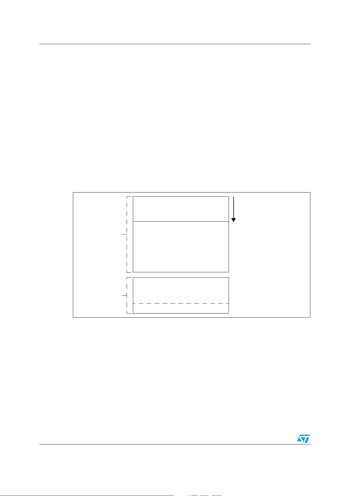
Product overview STM8AF61xx, STM8AF62xx
Programmable area
Data
UBC area
Flash program memory area
Data memory area (1 Kbytes)
EEPROM
Remains write protected during IAP
memory
Write access possible for IAP
Option bytes
Flash
program
memory
maximum 32 Kbytes
5.4.2 Write protection (WP)
Write protection in application mode is intended to avoid unintentional overwriting of the
memory. The write protection can be removed temporarily by executing a specific sequence
in the user software.
5.4.3 Protection of user boot code (UBC)
If the user chooses to update the Flash program memory using a specific boot code to
perform in application programming (IAP), this boot code needs to be protected against
unwanted modification.
In the STM8A a memory area of up to 32 Kbytes can be protected from overwriting at user
option level. Other than the standard write protection, the UBC protection can exclusively be
modified via the debug interface, the user software cannot modify the UBC protection status.
The UBC memory area contains the reset and interrupt vectors and its size can be adjusted
in increments of 512 bytes by programming the UBC and NUBC option bytes
(see Section 9: Option bytes on page 41).
Figure 2. Flash memory organization of STM8A products
5.4.4 Read-out protection (ROP)
The STM8A provides a read-out protection of the code and data memory which can be
activated by an option byte setting (see the ROP option byte in section 10).
The read-out protection prevents reading and writing Flash program memory, data memory
and option bytes via the debug module and SWIM interface. This protection is active in all
device operation modes. Any attempt to remove the protection by overwriting the ROP
option byte triggers a global erase of the program and data memory.
The ROP circuit may provide a temporary access for debugging or failure analysis. The
temporary read access is protected by a user defined, 8-byte keyword stored in the option
14/89 Doc ID 14952 Rev 6
byte area. This keyword must be entered via the SWIM interface to temporarily unlock the
device.

STM8AF61xx, STM8AF62xx Product overview
If desired, the temporary unlock mechanism can be permanently disabled by the user
through OPT6/NOPT6 option bytes.
5.5 Clock controller
The clock controller distributes the system clock coming from different oscillators to the core
and the peripherals. It also manages clock gating for low-power modes and ensures clock
robustness.
5.5.1 Features
● Clock sources:
– 16 MHz high-speed internal RC oscillator (HSI)
– 128 kHz low-speed internal RC (LSI)
– 1-16 MHz high-speed external crystal (HSE)
– Up to 16 MHz high-speed user-external clock (HSE user-ext)
● Reset: After reset the microcontroller restarts by default with an internal 2-MHz clock
(16 MHz/8). The clock source and speed can be changed by the application program
as soon as the code execution starts.
● Safe clock switching: Clock sources can be changed safely on the fly in Run mode
through a configuration register. The clock signal is not switched until the new clock
source is ready. The design guarantees glitch-free switching.
● Clock management: To reduce power consumption, the clock controller can stop the
clock to the core or individual peripherals.
● Wakeup: In case the device wakes up from low-power modes, the internal RC
oscillator (16 MHz/8) is used for quick startup. After a stabilization time, the device
switches to the clock source that was selected before Halt mode was entered.
● Clock security system (CSS): The CSS permits monitoring of external clock sources
and automatic switching to the internal RC (16 MHz/8) in case of a clock failure.
● Configurable main clock output (CCO): This feature permits to outputs a clock signal
for use by the application.
5.5.2 16 MHz high-speed internal RC oscillator (HSI)
● Default clock after reset 2 MHz (16 MHz/8)
● Fast wakeup time
User trimming
The register CLK_HSITRIMR with three trimming bits plus one additional bit for the sign
permits frequency tuning by the application program. The adjustment range covers all
possible frequency variations versus supply voltage and temperature. This trimming does
not change the initial production setting.
For reason of compatibility with other devices from the STM8A family, a special mode
with only two trimming bits plus sign can be selected. This selection is controlled
with the HSITRIM0 bit in the option byte registers OPT3 and NOPT3.
Doc ID 14952 Rev 6 15/89
Product overview STM8AF61xx, STM8AF62xx
5.5.3 128 kHz low-speed internal RC oscillator (LSI)
The frequency of this clock is 128 kHz and it is independent from the main clock. It drives
the independent watchdog or the AWU wakeup timer.
In systems which do not need independent clock sources for the watchdog counters, the
128 kHz signal can be used as the system clock. This configuration has to be enabled by
setting an option byte (OPT3/OPT3N, bit LSI_EN).
5.5.4 16 MHz high-speed external crystal oscillator (HSE)
The external high-speed crystal oscillator can be selected to deliver the main clock in
normal Run mode. It operates with quartz crystals and ceramic resonators.
● Frequency range: 1 MHz to 16 MHz
● Crystal oscillation mode: preferred fundamental
● I/Os: standard I/O pins multiplexed with OSCIN, OSCOUT
5.5.5 External clock input
An external clock signal can be applied to the OSCIN input pin of the crystal oscillator. The
frequency range is 0 to 16 MHz.
5.5.6 Clock security system (CSS)
The clock security system protects against a system stall in case of an external crystal clock
failure.
In case of a clock failure an interrupt is generated and the high-speed internal clock (HSI) is
automatically selected with a frequency of 2 MHz (16 MHz/8).
Table 4. Peripheral clock gating bit assignments in CLK_PCKENR1/2 registers
Bit
PCKEN17 TIM1 PCKEN13 LINUART PCKEN27 Reserved PCKEN23 ADC
PCKEN16 TIM3 PCKEN12 Reserved PCKEN26 Reserved PCKEN22 AWU
PCKEN15 TIM2 PCKEN11 SPI PCKEN25 Reserved PCKEN21 Reserved
PCKEN14 TIM4 PCKEN10 I
Peripheral
clock
Bit
Peripheral
clock
2
C PCKEN24 Reserved PCKEN20 Reserved
Bit
Peripheral
clock
Bit
Peripheral
clock
16/89 Doc ID 14952 Rev 6

STM8AF61xx, STM8AF62xx Product overview
5.6 Low-power operating modes
For efficient power management, the application can be put in one of four different low
power modes. You can configure each mode to obtain the best compromise between lowest
power consumption, fastest start-up time and available wakeup sources.
● Wait mode
In this mode, the CPU is stopped but peripherals are kept running. The wakeup is
performed by an internal or external interrupt or reset.
● Active-halt mode with regulator on
In this mode, the CPU and peripheral clocks are stopped. An internal wakeup is
generated at programmable intervals by the auto wake up unit (AWU). The main
voltage regulator is kept powered on, so current consumption is higher than in Activehalt mode with regulator off, but the wakeup time is faster. Wakeup is triggered by the
internal AWU interrupt, external interrupt or reset.
● Active-halt mode with regulator off
This mode is the same as Active-halt with regulator on, except that the main voltage
regulator is powered off, so the wake up time is slower.
● Halt mode
CPU and peripheral clocks are stopped, the main voltage regulator is powered off.
Wakeup is triggered by external event or reset.
In all modes the CPU and peripherals remain permanently powered on, the system clock is
applied only to selected modules. The RAM content is preserved and the brown-out reset
circuit remains activated.
5.7 Timers
5.7.1 Watchdog timers
The watchdog system is based on two independent timers providing maximum security to
the applications. The watchdog timer activity is controlled by the application program or
option bytes. Once the watchdog is activated, it cannot be disabled by the user program
without going through reset.
Window watchdog timer
The window watchdog is used to detect the occurrence of a software fault, usually
generated by external interferences or by unexpected logical conditions, which cause the
application program to abandon its normal sequence.
The window function can be used to trim the watchdog behavior to match the application
timing perfectly. The application software must refresh the counter before time-out and
during a limited time window. If the counter is refreshed outside this time window, a reset is
issued.
Doc ID 14952 Rev 6 17/89
Product overview STM8AF61xx, STM8AF62xx
Independent watchdog timer
The independent watchdog peripheral can be used to resolve malfunctions due to hardware
or software failures.
It is clocked by the 128 kHz LSI internal RC clock source, and thus stays active even in case
of a CPU clock failure. If the hardware watchdog feature is enabled through the device
option bits, the watchdog is automatically enabled at power-on, and generates a reset
unless the key register is written by software before the counter reaches the end of count.
5.7.2 Auto-wakeup counter
This counter is used to cyclically wakeup the device in Active-halt mode. It can be clocked by
the internal 128 kHz internal low-frequency RC oscillator or external clock.
LSI clock can be internally connected to TIM3 input capture channel 1 for calibration.
5.7.3 Beeper
This function generates a rectangular signal in the range of 1, 2 or 4 kHz which can be
output on a pin. This is useful when audible sounds without interference need to be
generated for use in the application.
5.7.4 Advanced control and general purpose timers
STM8A devices described in this datasheet, contain up to three 16-bit advanced control and
general purpose timers providing nine CAPCOM channels in total. A CAPCOM channel can
be used either as input compare, output compare or PWM channel. These timers are
named TIM1, TIM2 and TIM3.
Table 5. Advanced control and general purpose timers
Timer
TIM1 16-bit Up/down 1 to 65536 4 3 Yes Yes Yes Yes
TIM2 16-bit Up
TIM3 16-bit Up
Counter
width
Counter
type
Prescaler
factor
n
2
n = 0 to 15
n
2
n = 0 to 15
Channels
3 None No No No No
2 None No No No No
Inverted
outputs
Repetition
counter
trigger
unit
External
trigger
Break
input
18/89 Doc ID 14952 Rev 6
STM8AF61xx, STM8AF62xx Product overview
TIM1: Advanced control timer
This is a high-end timer designed for a wide range of control applications. With its
complementary outputs, dead-time control and center-aligned PWM capability, the field of
applications is extended to motor control, lighting and bridge driver.
● 16-bit up, down and up/down AR (auto-reload) counter with 16-bit fractional prescaler.
● Four independent CAPCOM channels configurable as input capture, output compare,
PWM generation (edge and center aligned mode) and single pulse mode output
● Trigger module which allows the interaction of TIM1 with other on-chip peripherals. In
the present implementation it is possible to trigger the ADC upon a timer event.
● External trigger to change the timer behavior depending on external signals
● Break input to force the timer outputs into a defined state
● Three complementary outputs with adjustable dead time
● Interrupt sources: 4 x input capture/output compare, 1 x overflow/update, 1 x break
TIM2 and TIM3: 16-bit general purpose timers
● 16-bit auto-reload up-counter
● 15-bit prescaler adjustable to fixed power of two ratios 1…32768
● Timers with three or two individually configurable CAPCOM channels
● Interrupt sources: 2 or 3 x input capture/output compare, 1 x overflow/update
5.7.5 Basic timer
The typical usage of this timer (TIM4) is the generation of a clock tick.
Table 6. TIM4
Timer
TIM4 8-bit Up
Counter
width
● 8-bit auto-reload, adjustable prescaler ratio to any power of two from 1 to 128
● Clock source: master clock
● Interrupt source: 1 x overflow/update
Counter
type
Prescaler
factor
n
2
n = 0 to 7
Channels
Inverted
outputs
Repetition
counter
trigger
unit
External
trigger
0 None No No No No
Break
input
Doc ID 14952 Rev 6 19/89
Product overview STM8AF61xx, STM8AF62xx
5.8 Analog-to-digital converter (ADC)
The STM8A products described in this datasheet contain a 10-bit successive approximation
ADC with up to 16 multiplexed input channels, depending on the package.
The ADC name differs between the datasheet and the STM8A/S reference manual (see
Ta bl e 7).
Table 7. ADC naming
Peripheral name in datasheet
Peripheral name in reference manual
(RM0016)
ADC ADC1
ADC features
● 10-bit resolution
● Single and continuous conversion modes
● Programmable prescaler: f
● Conversion trigger on timer events and external events
● Interrupt generation at end of conversion
● Selectable alignment of 10-bit data in 2 x 8 bit result register
● Shadow registers for data consistency
● ADC input range: V
●
Analog watchdog
● Schmitt-trigger on analog inputs can be disabled to reduce power consumption
● Scan mode (single and continuous)
● Dedicated result register for each conversion channel
● Buffer mode for continuous conversion
SSA
MASTER
≤ VIN ≤ V
Note: An additional AIN12 analog input is not selectable in ADC scan mode or with analog
watchdog. Values converted from AIN12 are stored only into the ADC_DRH/ADC_DRL
registers.
divided by 2 to 18
DDA
5.9 Communication interfaces
The following sections give a brief overview of the communication peripheral. Some
peripheral names differ between the datasheet and the STM8A/S reference manual (see
Ta bl e 8).
Table 8. Communication peripheral naming correspondence
Peripheral name in datasheet
LINUART UART2
20/89 Doc ID 14952 Rev 6
Peripheral name in reference manual
(RM0016)

STM8AF61xx, STM8AF62xx Product overview
5.9.1 Serial peripheral interface (SPI)
The devices covered by this datasheet contain one SPI. The SPI is available on all the
supported packages.
● Maximum speed: 10 Mbit/s or f
● Full duplex synchronous transfers
● Simplex synchronous transfers on two lines with a possible bidirectional data line
● Master or slave operation - selectable by hardware or software
● CRC calculation
● 1 byte Tx and Rx buffer
● Slave mode/master mode management by hardware or software for both master and
MASTER
slave
● Programmable clock polarity and phase
● Programmable data order with MSB-first or LSB-first shifting
● Dedicated transmission and reception flags with interrupt capability
● SPI bus busy status flag
● Hardware CRC feature for reliable communication:
– CRC value can be transmitted as last byte in Tx mode
– CRC error checking for last received byte
/2 both for master and slave
5.9.2 Inter integrated circuit (I2C) interface
The devices covered by this datasheet contain one I2C interface. The interface is available
on all the supported packages.
2
● I
C master features:
– Clock generation
– Start and stop generation
2
● I
C slave features:
– Programmable I
– Stop bit detection
● Generation and detection of 7-bit/10-bit addressing and general call
● Supports different communication speeds:
– Standard speed (up to 100 kHz),
– Fast speed (up to 400 kHz)
● Status flags:
– Transmitter/receiver mode flag
– End-of-byte transmission flag
2
–I
C busy flag
● Error flags:
– Arbitration lost condition for master mode
– Acknowledgement failure after address/data transmission
– Detection of misplaced start or stop condition
– Overrun/underrun if clock stretching is disabled
2
C address detection
Doc ID 14952 Rev 6 21/89

Product overview STM8AF61xx, STM8AF62xx
● Interrupt:
– Successful address/data communication
– Error condition
– Wakeup from Halt
● Wakeup from Halt on address detection in slave mode
5.9.3 Universal asynchronous receiver/transmitter with LIN support (LINUART)
The devices covered by this datasheet contain one LINUART interface. The interface is
available on all the supported packages. The LINUART is an asynchronous serial
communication interface which supports extensive LIN functions tailored for LIN slave
applications. In LIN mode it is compliant to the LIN standards rev 1.2 to rev 2.1.
Detailed feature list:
LIN mode
Master mode:
● LIN break and delimiter generation
● LIN break and delimiter detection with separate flag and interrupt source for read back
checking.
Slave mode:
● Autonomous header handling – one single interrupt per valid header
● Mute mode to filter responses
● Identifier parity error checking
● LIN automatic resynchronization, allowing operation with internal RC oscillator (HSI)
clock source
● Break detection at any time, even during a byte reception
● Header errors detection:
– Delimiter too short
– Synch field error
– Deviation error (if automatic resynchronization is enabled)
– Framing error in synch field or identifier field
– Header time-out
22/89 Doc ID 14952 Rev 6

STM8AF61xx, STM8AF62xx Product overview
UART mode
● Full duplex, asynchronous communications - NRZ standard format (mark/space)
● High-precision baud rate generator
– A common programmable transmit and receive baud rates up to f
● Programmable data word length (8 or 9 bits) – 1 or 2 stop bits – parity control
● Separate enable bits for transmitter and receiver
● Error detection flags
● Reduced power consumption mode
● Multi-processor communication - enter mute mode if address match does not occur
● Wakeup from mute mode (by idle line detection or address mark detection)
● Two receiver wakeup modes:
MASTER
/16
– Address bit (MSB)
– Idle line
5.10 Input/output specifications
The product features four different I/O types:
● Standard I/O 2 MHz
● Fast I/O up to 10 MHz
● High sink 8 mA, 2 MHz
● True open drain (I
2
C interface)
To decrease EMI (electromagnetic interference), high sink I/Os have a limited maximum
slew rate. The rise and fall times are similar to those of standard I/Os.
The analog inputs are equipped with a low leakage analog switch. Additionally, the schmitttrigger input stage on the analog I/Os can be disabled in order to reduce the device standby
consumption.
STM8A I/Os are designed to withstand current injection. For a negative injection current of
4
mA, the resulting leakage current in the adjacent input does not exceed 1 µA. Thanks to
this feature, external protection diodes against current injection are no longer required.
Doc ID 14952 Rev 6 23/89
Pinouts and pin description STM8AF61xx, STM8AF62xx
I2C_SCL/AIN4/PB4
TIM1_ETR/AIN3/PB3
TIM1_CH3N/AIN2/PB2
TIM1_CH2N/AIN1/PB1
TIM1_CH1N/AIN0/PB0
V
DDA
V
SSA
I2C_SDA/AIN5/PB5
32 31 3029 28 2726 25
24
23
22
21
20
19
18
17
9 101112131415
16
1
2
3
4
5
6
7
8
VCAP
V
DD
V
DDIO
AIN12/PF4
NRST
OSCIN/PA1
OSCOUT/PA2
V
SS
PC3 (HS)/TIM1_CH3
PC2 (HS)/TIM1_CH2
PC1 (HS)/TIM1_CH1
PE5/SPI_NSS
PC7/SPI_MISO
PC6/SPI_MOSI
PC5/SPI_SCK
PC4 (HS)/TIM1_CH4
PD3 (HS)/TIM2_CH2/ADC_ETR
PD2 (HS)/TIM3_CH1/TIM2_CH3
PD1 (HS)/SWIM
PD0 (HS)/TIM3_CH2/CLK_CCO/TIM1_BRK
PD7/TLI
PD6/LINUART_RX
PD5/LINUART_TX
PD4 (HS)/TIM2_CH1/BEEP
6 Pinouts and pin description
6.1 Package pinouts
Figure 3. VFQFPN/LQFP 32-pin pinout
1. (HS) high sink capability.
24/89 Doc ID 14952 Rev 6

STM8AF61xx, STM8AF62xx Pinouts and pin description
44 4342 4140 3938 37
36
35
34
33
32
31
30
29
28
27
26
25
24
23
12
13 14 1516 1718 1920 21 22
1
2
3
4
5
6
7
8
9
10
11
48 47 46 45
PA6
AIN8/PE7
PC1 (HS)/TIM1_CH1
PE5/SPI_NSS
PG1
AIN9/PE6
PD3 (HS)/TIM2_CH2/ADC_ETR
PD2 (HS)/TIM3_CH1
PE0/CLK_CCO
PE1/I
2
C_SCL
PE2/I
2
C_SDA
PE3/TIM1_BKIN
PD7/TLI
PD6/LINUART_RX
PD5/LINUART_TX
PD4 (HS)/TIM2_CH1/BEEP
PD1 (HS)/SWIM
PD0 (HS)/TIM3_CH2
V
SSIO_2
PC5/SPI_SCK
PC4 (HS)/TIM1_CH4
PC3 (HS)/TIM1_CH3
PC2 (HS)/TIM1_CH2
PG0
PC7/SPI_MISO
PC6/SPI_MOSI
V
DDIO_2
AIN7/PB7
AIN6/PB6
AIN5/PB5
AIN4/PB4
TIM1_ETR/AIN3/PB3
TIM1_CH3N/AIN2/PB2
TIM1_CH2N/AIN1/PB1
TIM1_CH1N/AIN0/PB0
V
DDA
V
SSA
V
SS
VCAP
V
DD
V
DDIO_1
TIM2_CH3/PA3
PA4
PA5
NRST
OSCIN/PA1
OSCOUT/PA2
V
SSIO_1
Figure 4. LQFP 48-pin pinout
2. (HS) high sink capability.
Table 9. Legend/abbreviation
Type I= input, O = output, S = power supply
Level Input CM = CMOS (standard for all I/Os)
Output HS = High sink (8 mA)
Output speed O1 = Standard (up to 2 MHz)
O2 = Fast (up to 10 MHz)
O3 = Fast/slow programmability with slow as default state after reset
O4 = Fast/slow programmability with fast as default state after reset
Port and control
configuration
Reset state
Input float = floating, wpu = weak pull-up
Output T = true open drain, OD = open drain, PP = push pull
Bold X (pin state after reset release).
Unless otherwise specified, the pin state is the same during the reset phase (i.e.
“under reset”) and after internal reset release (i.e. at reset state).
Doc ID 14952 Rev 6 25/89
Pinouts and pin description STM8AF61xx, STM8AF62xx
Table 10. STM8AF61xx/62xx (32 Kbytes) microcontroller pin description
Pin
number
Pin name
LQFP48
Input Output
Type
wpu
floating
Ext. interrupt
High sink
Speed
OD
PP
Main function
Default alternate
(after reset)
(1)(2)
function
VFQFPN/LQFP32
1 1 NRST I/O - X - - - - - Reset —
(3)
22PA1/OSCIN
I/O X X- -O1XXPor t A1 Resonator/crystal in —
3 3 PA2/OSCOUT I/O X XX-O1XXPort A2 Resonator/crystal out —
4-V
54V
SSIO_1
SS
S - - - - - - - I/O ground —
S - - - - - - - Digital ground —
6 5 VCAP S - - - - - - - 1.8 V regulator capacitor —
76V
87V
DD
DDIO_1
- 8 PF4/AIN12
(4)(5)
S - - - - - - - Digital power supply —
S - - - - - - - I/O power supply —
I/O X X-O1XXPort F4 Analog input 12 —
9 - PA3/TIM2_CH3 I/O X XX -O1XXPort A3 Timer 2 - channel 3
Alternate
function after
remap
[option bit]
TIM3_CH1
[AFR1]
10 - PA4 I/O X XX-O3XXPor t A4 —
11 - PA5 I/O X XX-O3XXPor t A5 —
12 - PA6 I/O X XX-O3XXPor t A6 —
13 9 V
14 10 V
DDA
SSA
S - - - - - - - Analog power supply —
S - - - - - - - Analog ground —
15 - PB7/AIN7 I/O X XX -O1XXPort B7 Analog input 7 —
16 - PB6/AIN6 I/O X XX -O1XXPort B6 Analog input 6 —
17 11 PB5/AIN5 I/O X XX -O1XXPort B5 Analog input 5
18 12 PB4/AIN4 I/O X XX -O1XXPort B4 Analog input 4
19 13 PB3/AIN3 I/O X XX -O1XXPort B3 Analog input 3
I
[AFR6]
I
[AFR6]
TIM1_ETR
[AFR5]
TIM1_
20 14 PB2/AIN2 I/O X XX -O1XXPort B2 Analog input
NCC3
[AFR5]
TIM1_
21 15 PB1/AIN1 I/O X XX -O1XXPort B1 Analog input 1
NCC2
[AFR5]
TIM1_
22 16 PB0/AIN0 I/O X XX -O1XXPort B0 Analog input 0
NCC1
[AFR5]
2
C_SDA
2
C_SCL
26/89 Doc ID 14952 Rev 6
STM8AF61xx, STM8AF62xx Pinouts and pin description
Table 10. STM8AF61xx/62xx (32 Kbytes) microcontroller pin description
Pin
number
Pin name
LQFP48
Input Output
Typ e
wpu
floating
Ext. interrupt
High sink
OD
Speed
PP
Main function
Default alternate
(after reset)
(1)(2)
function
(continued)
VFQFPN/LQFP32
23 - PE7/AIN8 I/O X X-O1XXPort E7 Analog input 8 —
24 PE6/AIN9 I/O X XX -O1XXPort E7 Analog input 9 —
25 17 PE5/SPI_NSS I/O X XX -O1XXPort E5 SPI master/slave select —
26 18 PC1/TIM1_CH1 I/O X XXHSO3XXPort C1 Timer 1 - channel 1 —
27 19 PC2/TIM1_CH2 I/O X XXHSO3XXPort C2 Timer 1- channel 2 —
28 20 PC3/TIM1_CH3 I/O X XXHSO3XXPort C3 Timer 1 - channel 3 —
29 21 PC4/TIM1_CH4 I/O X XXHSO3XXPort C4 Timer 1 - channel 4 —
30 22 PC5/SPI_SCK I/O X XX O3XXPort C5 SPI clock —
31 - V
32 - V
SSIO_2
DDIO_2
33 23 PC6/SPI_MOSI I/O X XX-O3XXPort C6
S - - - - - - - I/O ground —
S - - - - - - - I/O power supply —
SPI master out/
slave in
Alternate
function after
remap
[option bit]
—
34 24 PC7/SPI_MISO I/O X XX-O3XXPort C7 SPI master in/ slave out —
35 - PG0 I/O X X--O1XXPort G0 -—
36 - PG1 I/O X X--O1XXPort G1 -—
37 - PE3/TIM1_BKIN I/O X XX -O1XXPort E3 Timer 1 - break input —
2
38 - PE2/I
39 - PE1/I
C_SDA I/O X -X-O1T
2
C_SCL I/O X -X-O1T
40 - PE0/CLK_CCO I/O X XX -O3XXPort E0
(6)
- Port E2 I2C data —
(6)
- Port E1 I2C clock —
Configurable clock
output
—
TIM1_BKIN
41 25 PD0/TIM3_CH2 I/O X XXHSO3XXPort D0 Timer 3 - channel 2
[AFR3]/
CLK_CCO
[AFR2]
42 26 PD1/SWIM
43 27 PD2/TIM3_CH1 I/O X XXHSO3XXPort D2 Timer 3 - channel 1
44 28 PD3/TIM2_CH2 I/O X XXHSO3XXPort D3 Timer 2 - channel 2
45 29
46 30
PD4/TIM2_CH1/
BEEP
PD5/
LINUART_TX
(7)
I/O X X XHSO4X XPort D1 SWIM data interface —
TIM2_CH3
[AFR1]
ADC_ETR
[AFR0]
I/O X XXHSO3XXPort D4 Timer 2 - channel 1
BEEP output
[AFR7]
I/O X XX -O1XXPort D5 LINUART data transmit —
Doc ID 14952 Rev 6 27/89
 Loading...