

1/4 to 1/11-duty VFD controller/driver
General features
■ Many display modes (11 segments & 11 digits
to 16 segments & 4 digits)
■ Key scanning (6 x 4 matrix)
■ Dimming circuit (eight steps)
■ High-voltage output (V
■ LED ports (4 chs, 20mA max)
■ General purpose input port (4 bits)
■ No external resistor necessary for driver output
(P-channel open drain + pull down resistor
output)
■ Serial interface (CLK, STB, D
– 35V max)
DD
IN
, D
OUT
)
STM86312
PQFP44
Description
The STM86312 is a VFD (Vacuum Fluorescent
Display) controller/driver that is driven on a 1/4 to
1/11-duty factor . It consists of 1 1-segments output
lines, 6 grid output lines, 5 segments/grid output
drive lines, a display memory, a control circuit,
and a key scan circuit. Serial data are input to the
STM86312 through a three-line serial interface.
This VFD controller/driver is ideal as a peripheral
device for a single-chip microcomputer.
Order codes
Part number Temperature range Package Tube
STM86312 -40 to 85 °C PQFP44 Tray
March 2006 Rev 2 1/24
www.st.com
24

Contents STM86312
Contents
1 Block diagram . . . . . . . . . . . . . . . . . . . . . . . . . . . . . . . . . . . . . . . . . . . . . . 3
2 Pin settings . . . . . . . . . . . . . . . . . . . . . . . . . . . . . . . . . . . . . . . . . . . . . . . . 4
2.1 Pin connection . . . . . . . . . . . . . . . . . . . . . . . . . . . . . . . . . . . . . . . . . . . . . . 4
2.2 Pin description . . . . . . . . . . . . . . . . . . . . . . . . . . . . . . . . . . . . . . . . . . . . . . 5
3 Maximum rating . . . . . . . . . . . . . . . . . . . . . . . . . . . . . . . . . . . . . . . . . . . . . 6
3.1 Thermal data . . . . . . . . . . . . . . . . . . . . . . . . . . . . . . . . . . . . . . . . . . . . . . . 6
3.2 Recommended operating conditions . . . . . . . . . . . . . . . . . . . . . . . . . . . . . 6
4 Electrical characteristics . . . . . . . . . . . . . . . . . . . . . . . . . . . . . . . . . . . . . 8
5 Display RAM address and display mode . . . . . . . . . . . . . . . . . . . . . . . 10
6 LED port . . . . . . . . . . . . . . . . . . . . . . . . . . . . . . . . . . . . . . . . . . . . . . . . . . 12
7 SW data . . . . . . . . . . . . . . . . . . . . . . . . . . . . . . . . . . . . . . . . . . . . . . . . . . 13
8 Commands . . . . . . . . . . . . . . . . . . . . . . . . . . . . . . . . . . . . . . . . . . . . . . . . 14
8.1 Display mode setting command . . . . . . . . . . . . . . . . . . . . . . . . . . . . . . . . 14
8.2 Data setting comma nd . . . . . . . . . . . . . . . . . . . . . . . . . . . . . . . . . . . . . . . 15
8.3 Address setting command . . . . . . . . . . . . . . . . . . . . . . . . . . . . . . . . . . . . 15
8.4 Display control com mand . . . . . . . . . . . . . . . . . . . . . . . . . . . . . . . . . . . . . 16
9 Serial communication format . . . . . . . . . . . . . . . . . . . . . . . . . . . . . . . . . 17
10 Application . . . . . . . . . . . . . . . . . . . . . . . . . . . . . . . . . . . . . . . . . . . . . . . . 19
11 Mechanical data . . . . . . . . . . . . . . . . . . . . . . . . . . . . . . . . . . . . . . . . . . . . 21
12 Revision history . . . . . . . . . . . . . . . . . . . . . . . . . . . . . . . . . . . . . . . . . . . 23
2/24

STM86312 Block diagram
1 Block diagram
Figure 1. Block diagram
3/24
Pin settings STM86312
2 Pin settings
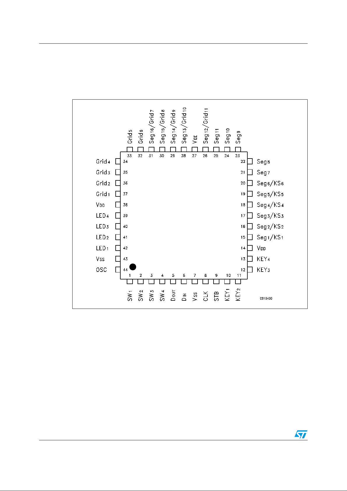
2.1 Pin connection
Figure 2. Pin connection
4/24
STM86312 Pin se tt i ngs
2.2 Pin description
Table 1. Pin description
Pin N° Symbol Name and function
1, 2, 3, 4
SW1, SW2,
SW3, SW4
General-purpose switch inputs.
5
6
D
OUT
D
IN
8CLK
9STB
10, 11, 12, 13
14, 38
15, 16, 17,
18, 19, 20
21, 22, 23,
24, 25
26, 28, 29,
30, 31
32, 33, 34,
35, 36, 37
KEY1, KEY2,
KEY3, KEY4
V
DD
SEG1/KS1 to
SEG6/KS6
SEG7 to SEG11 Segment output pins.
SEG12/GRID11 to
SEG16/GRID7
GRID1 to GRID 6 Grid output pins.
Output serial data at falling edge of the shift clock, starting
from lower bit. This is N-ch open-drain output pin.
Input serial data at rising edge of the shift clock, starting from
lower bit.
Reads serial dat a at rising edge, and outputs data at falling
edge.
Initializes serial interface at risi ng or falling edge to make
STM86312 waiting f or reception of command. Data input after
STB has fall en are pr ocessed as a command. Whi le co mmand
data are processed, current processing is sto pped, and the
serial interfac e is initi alize d. While STB is high, CLK is ignored.
Input data to these pins are latched at end of the display cycle.
5V ± 10%.
Segment output pin s (Dual function as key source).
These pins are selectable for segment or grid driving.
39, 40, 41, 42 LED1 to LED4 CMOS outputs. +20 mA max.
7, 43
27
V
SS
V
EE
Connect this pin to system GND.
Pull-dow n le vel . V
- 35V max .
DD
44 OSC Connect to an external resistor.
5/24

Maximum rating STM86312
3 Maximum rating
Stressing the device above the rating listed in the “Absolute Max imum Ratings” table may
cause permanent damage to the device. These are stress ratings only and operation of the
device at these or any other conditions above those indicated in the Operating sections of
this specification is not implied. Exposure to Absolute Maximum Rating conditions for
extended periods may affect device reliability. Refer also to the STMicroelectronics SURE
Program and other relevant quality documents.
Table 2. Absolute maximum rati ngs
Symbol Parameter Value Unit
V
V
V
I
I
Logic Supply Voltage -0.5 to 7 V
DD
Driver Supply Voltage
EE
V
Logic Input Voltage
I
VFD Driver Output Voltage
O2
LED Driver Output Current 25 mA
O1
VFD Driver Output Current
O2
T
Operating Ambient Temperature -40 to 85 °C
A
3.1 Thermal data
Table 3. Therma l data
Symbol Parameter Value Unit
R
thJC
Thermal Resistance Junction-case 56 °C/W
3.2 Recommended operating conditions
V
+0.5 to VDD-40
DD
-0.5 to V
-0.5 to VDD+0.5
V
EE
-40 (Grid)
-15 (Segment)
DD
+0.5
V
V
V
mA
Table 4. Recommended operating conditions
Symbol Parameter Min Typ Max Unit
V
DD
V
IH
V
IL
V
EE
6/24
Logic Supply Voltage 4.5 5 5.5 V
High Level Input Voltage 0.7xV
Low Level Input Voltage 0 0.3xV
Driver Supply Voltage 0 VDD-35 V
DD
V
DD
DD
V
V

STM86312 Maximum rating
Maximum power consumption P
= VFD driver dissipation + RL dissipation + LED driver
MAX
dissipation + dynamic power consumption.
Where segment current = 3 mA, grid current = 15 mA, and LED current = 20 mA,
VFD driver dissipation = number of segments x 6 + number of grids/(number of grids + 1) x
30 (mW)
dissipation = (VDD - VEE)2/50 x (segment + 1) (mW)
R
L
LED driver dissipation = number of LEDs x 20 (mW)
Dynamic power consumption = V
x 5 (mW)
DD
Example
Where V
= -25 V, V
EE
= 5 V, and in 16-segment and 6-digit modes,
DD
VFD driver dissipation = 16 x 6 + 6/7 x 30 = 122
dissipation = 302/50 x 17 = 306
R
L
LED driver dissipation = 4 x 20 = 80
Dynamic power consumption = 5 x 5 = 25
Total 553 mW.
7/24

Electrical characteristics STM86312
4 Electrical characteristics
Table 5. Electrical characteristics (V
to 70°C, unless otherwise noted. Typical values are at T
Symbol Parameter Test Conditions
V
V
V
I
OH21
High Level Output Voltage LED1-LED4, I
OH1
Low Level Output Voltage LED1-LED4, I
OL1
Low Level Output Voltage D
OL2
High Level Output Current VO = V
= 4.5 to 5.5V, V
DD
, I
OUT
OL2
DD
Seg11
= 0V, V
SS
= 25°C)
A
EE
= V
DD
- 35V, TA = -20
Value
Min. Typ. Max.
=-1mA 0.9V
OH1
=20mA 1 V
OL1
DD
= 4mA 0.4 V
- 2V, Seg1 to
-3 mA
Unit
V
I
OH22
High Level Output Current VO = V
- 2V, Grid1 to
DD
Grid6,
Seg12/Grid11 to
Seg16/Grid7
I
OLEAK
Driver Leakage Current VO = V
R
Output Pull-Down
L
- 35V, driver off -10 µA
DD
Driver Output 50 1 00 150 kΩ
Resistor
I
V
V
V
HYS
I
DDdyn
Input Current VI = V
I
High Level Input Voltage 0.7V
IH
Low Level Input Voltage 0.3V
IL
Hysteresis Voltage CLK, DIN, STB 0.35 V
Dynamic Current
Under no load, display off 5 mA
DD
or V
SS
Consumption
Table 6. Switching characteristics (V
= 4.5 to 5.5V, VSS = 0V, V
DD
to 70°C, unless otherwise noted. Typical values are at T
Symbol Parameter Test Conditions
t
t
t
TZH1
t
TZH2
Propagation Delay CLK → D
PLZ
OUT
RL = 10 kΩ, CL = 15 pF
PZL
Rise Time CL = 300 pFSeg1 to Seg11 2 µs
Grid1 to Grid6,
Seg12/Grid11 to
Seg16/Grid7
= 25°C)
A
-15 mA
±1 µA
DD
V
V
DD
EE
= V
DD
- 35V, TA = -20
Value
Unit
Min. Typ. Max.
300 ns
100
0.5
t
THZ
f
MAX
Fall Time CL = 300 pF , Segn, Gridn 120 µs
Maximum Clock
Duty = 50% 1 MHz
Frequency
C
Inpu t C a pacita nce 15 pF
I
8/24
 Loading...