

STM809, STM810
STM811, STM812
Reset circuit
Features
■ Precision monitoring of 3 V, 3.3 V, and 5 V
supply voltages
■ Two output configurations
– Push-pull RST
– Push-pull RST output (STM810/812)
■ 140 ms reset pulse width (min)
■ Low supply current - 6 µA (typ)
■ Guaranteed RST/RST assertion down to
V
= 1.0 V
CC
■ Operating temperature:
–40 °C to 85 °C (industrial grade)
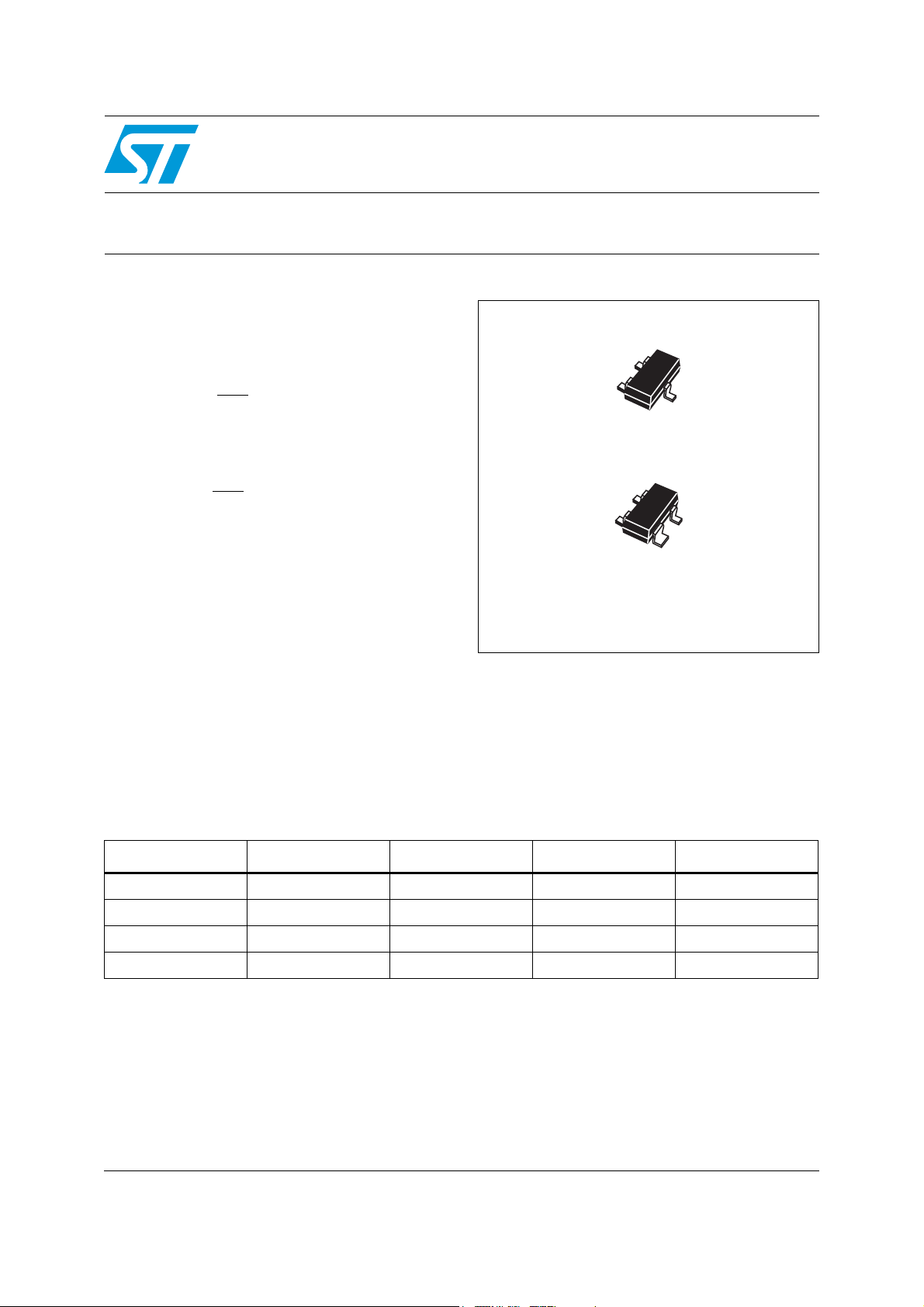
■ Lead-free, small SOT23 and SOT143 package
output (STM809/811)
SOT23-3 (WX)
SOT143-4 (W1)
Table 1. Device summary
Active-low reset Active-high reset Manual reset input Package
STM809 ✔ SOT23-3
STM810 ✔ SOT23-3
STM811 ✔✔SOT143-4
STM812 ✔✔SOT143-4
January 2010 Doc ID 9873 Rev 5 1/21
www.st.com
1

Contents STM809/810/811/812
Contents
1 Description . . . . . . . . . . . . . . . . . . . . . . . . . . . . . . . . . . . . . . . . . . . . . . . . . 5
2 Operation . . . . . . . . . . . . . . . . . . . . . . . . . . . . . . . . . . . . . . . . . . . . . . . . . . 7
2.1 Reset output . . . . . . . . . . . . . . . . . . . . . . . . . . . . . . . . . . . . . . . . . . . . . . . . 7
2.2 Push-button reset input (STM811/812) . . . . . . . . . . . . . . . . . . . . . . . . . . . 7
2.3 Negative-going V
2.4 Valid RST
output down to VCC = 0 V . . . . . . . . . . . . . . . . . . . . . . . . . . . . . 8
transients . . . . . . . . . . . . . . . . . . . . . . . . . . . . . . . . . . 7
CC
3 Typical operating characteristics . . . . . . . . . . . . . . . . . . . . . . . . . . . . . . 9
4 Maximum ratings . . . . . . . . . . . . . . . . . . . . . . . . . . . . . . . . . . . . . . . . . . . 12
5 DC and AC parameters . . . . . . . . . . . . . . . . . . . . . . . . . . . . . . . . . . . . . . 13
6 Package mechanical data . . . . . . . . . . . . . . . . . . . . . . . . . . . . . . . . . . . . 16
7 Part numbering . . . . . . . . . . . . . . . . . . . . . . . . . . . . . . . . . . . . . . . . . . . . 18
8 Revision history . . . . . . . . . . . . . . . . . . . . . . . . . . . . . . . . . . . . . . . . . . . 20
2/21 Doc ID 9873 Rev 5

STM809/810/811/812 List of tables
List of tables
Table 1. Device summary . . . . . . . . . . . . . . . . . . . . . . . . . . . . . . . . . . . . . . . . . . . . . . . . . . . . . . . . . . 1
Table 2. Signal names . . . . . . . . . . . . . . . . . . . . . . . . . . . . . . . . . . . . . . . . . . . . . . . . . . . . . . . . . . . . 5
Table 3. Absolute maximum ratings . . . . . . . . . . . . . . . . . . . . . . . . . . . . . . . . . . . . . . . . . . . . . . . . . 12
Table 4. Operating and AC measurement conditions . . . . . . . . . . . . . . . . . . . . . . . . . . . . . . . . . . . . 13
Table 5. DC and AC characteristics . . . . . . . . . . . . . . . . . . . . . . . . . . . . . . . . . . . . . . . . . . . . . . . . . 14
Table 6. SOT23-3 – 3-lead small outline transistor package mechanical data. . . . . . . . . . . . . . . . . 16
Table 7. SOT143-4 – 4-lead small outline transistor package mechanical data. . . . . . . . . . . . . . . . 17
Table 8. Ordering information scheme . . . . . . . . . . . . . . . . . . . . . . . . . . . . . . . . . . . . . . . . . . . . . . . 18
Table 9. Marking description . . . . . . . . . . . . . . . . . . . . . . . . . . . . . . . . . . . . . . . . . . . . . . . . . . . . . . . 19
Table 10. Document revision history . . . . . . . . . . . . . . . . . . . . . . . . . . . . . . . . . . . . . . . . . . . . . . . . . 20
Doc ID 9873 Rev 5 3/21

List of figures STM809/810/811/812
List of figures
Figure 1. Logic diagram (STM809/810) . . . . . . . . . . . . . . . . . . . . . . . . . . . . . . . . . . . . . . . . . . . . . . . . 5
Figure 2. Logic diagram (STM811/812) . . . . . . . . . . . . . . . . . . . . . . . . . . . . . . . . . . . . . . . . . . . . . . . . 5
Figure 3. SOT23-3 connections . . . . . . . . . . . . . . . . . . . . . . . . . . . . . . . . . . . . . . . . . . . . . . . . . . . . . . 6
Figure 4. SOT143-4 connections . . . . . . . . . . . . . . . . . . . . . . . . . . . . . . . . . . . . . . . . . . . . . . . . . . . . . 6
Figure 5. Block diagram . . . . . . . . . . . . . . . . . . . . . . . . . . . . . . . . . . . . . . . . . . . . . . . . . . . . . . . . . . . . 6
Figure 6. Hardware hookup . . . . . . . . . . . . . . . . . . . . . . . . . . . . . . . . . . . . . . . . . . . . . . . . . . . . . . . . . 6
Figure 7. Supply current vs. temperature, L/M/R/S/T (no load) . . . . . . . . . . . . . . . . . . . . . . . . . . . . . . 9
Figure 8. Power-down reset delay vs. temperature - V
Figure 9. Power-down reset delay vs. temperature - V
Figure 10. Power-up t
Figure 11. Normalized reset threshold vs. temperature. . . . . . . . . . . . . . . . . . . . . . . . . . . . . . . . . . . . 11
Figure 12. Max transient duration NOT causing reset pulse vs. reset comparator overdrive . . . . . . . 11
Figure 13. AC testing input/output waveforms . . . . . . . . . . . . . . . . . . . . . . . . . . . . . . . . . . . . . . . . . . . 13
Figure 14. MR timing waveform . . . . . . . . . . . . . . . . . . . . . . . . . . . . . . . . . . . . . . . . . . . . . . . . . . . . . . 13
Figure 15. SOT23-3 – 3-lead small outline transistor package outline . . . . . . . . . . . . . . . . . . . . . . . . 16
Figure 16. SOT143-4 – 4-lead small outline transistor package outline . . . . . . . . . . . . . . . . . . . . . . . 17
vs. temperature . . . . . . . . . . . . . . . . . . . . . . . . . . . . . . . . . . . . . . . . . . . . . . 10
rec
= VTH – VCC (L/M) . . . . . . . . . . . . . . . . . . . 9
OD
= VTH – VCC (R/S/T) . . . . . . . . . . . . . . . . 10
OD
4/21 Doc ID 9873 Rev 5
STM809/810/811/812 Description
1 Description
The STM809/810/811/812 microprocessor reset circuits are low-power supervisory devices
used to monitor power supplies. They perform a single function: asserting a reset signal
whenever the V
V
has risen above the preset threshold for a minimum period of time (t
CC
STM811/812 also provide a push-button reset input (MR
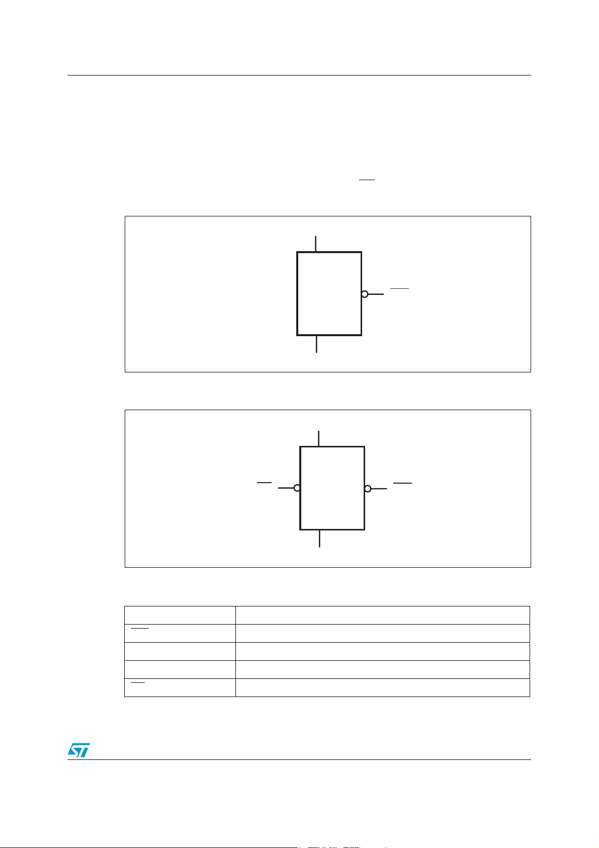
Figure 1. Logic diagram (STM809/810)
supply voltage drops below a preset value and keeping it asserted until
CC
rec
). The
).
V
CC
STM809/810
V
1. For STM810
Figure 2. Logic diagram (STM811/812)
MR
1. For STM812
STM811/812
RST (RST)
SS
V
CC
RST (RST)
V
SS
(1)
AI07832
(1)
AI07831
Table 2. Signal names
V
SS
RST Active-low reset output
(1)
RST
V
CC
(2)
MR
1. STM810/812 only
2. STM811/812 only
Ground
Active-high reset output
Supply voltage
Manual reset input
Doc ID 9873 Rev 5 5/21

Description STM809/810/811/812
Figure 3. SOT23-3 connections
V
SS
RST (RST)
(For STM810)
Figure 4. SOT143-4 connections
V
SS
RST (RST)
(For STM812)
Figure 5. Block diagram
V
CC
V
RST
(1)
MR
1
2
1
2
COMPARE
DEBOUNCE
3
4
3
V
V
CC
MR
CC
t
rec
Generator
RST
AI07833
AI07834
(2)
1. STM811/812 only
2. RST for STM810/812
Figure 6. Hardware hookup
V
CC
V
CC
STM809/810/
811/812
(2)
Push-button
RESET
1. STM809/811 only (RST for STM810/812)
2. STM811/812 only
MR
V
6/21 Doc ID 9873 Rev 5
SS
RST
(1)
MCU
RESET
Input
AI07835
V
CC
V
SS
AI07836

STM809/810/811/812 Operation
2 Operation
2.1 Reset output
The STM809/810/811/812 microprocessor reset circuit asserts a reset signal to the MCU
whenever V
(MR
) is taken low (see Figure 14 on page 13). RST (active high for STM810/812) is
guaranteed valid down to V
During power-up, once V
the reset time-out period, t
If V
drops below the reset threshold, RST goes low. Each time RST is asserted, it stays
CC
low for at least the reset time-out period. Any time V
internal timer clears. The reset timer starts when V
active-low reset (RST
2.2 Push-button reset input (STM811/812)
goes below the reset threshold (V
CC
= 1 V (0° to 70°C).
CC
exceeds the reset threshold an internal timer keeps RST low for
CC
. After this interval, RST returns high.
rec
) and active-high reset (RST) both source and sink current.
), or when the push-button reset input
RST
goes below the reset threshold, the
CC
returns above the reset threshold. The
CC
A logic low on MR asserts RST. RST remains asserted while MR is low, and for t
returns high. The MR
input has an internal 20 kΩ pull-up resistor, allowing it to be left open if
not used. This input can be driven with TTL/CMOS-logic levels or with open-drain/collector
outputs. Connect a normally open push-button switch from MR
reset function; external debounce circuitry is not required. If the device is used in a noisy
environment, connect a 0.1 µF capacitor from MR
immunity.
2.3 Negative-going VCC transients
The STM809/810/811/812 are relatively immune to negative-going VCC transients (glitches).
Figure 12 on page 11 shows typical transient duration versus reset comparator overdrive
(for which the STM809/810/811/812 will NOT generate a reset pulse). The graph was
generated using a negative pulse applied to V
threshold and ending below it by the magnitude indicated (comparator overdrive). The graph
indicates the maximum pulse width a negative V
reset pulse. As the magnitude of the transient increases (further below the threshold), the
maximum allowable pulse width decreases. Any combination of duration and overdrive
which lies under the curve will NOT generate a reset signal. Typically, a V
goes 100 mV below the reset threshold and lasts 20 µs or less will not cause a reset pulse.
A 0.1 µF bypass capacitor mounted as close as possible to the V
transient immunity.
rec
to GND to create a manual
to GND to provide additional noise
, starting at 0.5V above the actual reset
CC
transient can have without causing a
CC
transient that
CC
pin provides additional
CC
after it
Doc ID 9873 Rev 5 7/21

Operation STM809/810/811/812
2.4 Valid RST output down to VCC = 0 V
When VCC falls below 1 V, the RST (STM809/811) output no longer sinks current, but
becomes an open circuit. In most systems this is not a problem, as most MCUs do not
operate below 1 V. However, in applications where RST
pull-down resistor may be added to hold the RST
enough to not load the RST
100 kΩ resistor is recommended.
output, and still be small enough to pull the output to ground. A
output must be valid down to 0 V, a
output low. This resistor must be large
Note: The same situation applies for the active-high RST of the STM810/812. A 100 k
resistor to V
should be used if RST must remain valid for VCC < 1.0 V.
CC
Ω
pull-up
8/21 Doc ID 9873 Rev 5

STM809/810/811/812 Typical operating characteristics
3 Typical operating characteristics
Note: Typical values are at TA = 25 °C, VCC = 5 V for L/M versions, VCC = 3.3 V for T/S versions,
and V
Figure 7. Supply current vs. temperature, L/M/R/S/T (no load)
= 3.0 V for R versions.
CC
8.0
6.0
4.0
Supply Current (µA)
2.0
0.0
–40 –20 0 20 40 60 80
Temperature (°C)
1V
3V
3.6V
5.5V
AI07879
Figure 8. Power-down reset delay vs. temperature - V
140.00
120.00
100.00
80.00
60.00
40.00
Power-Down Reset Delay (µs)
20.00
0.00
–40 –20 0 20 40 60 80
Temperature (°C)
= VTH – VCC (L/M)
OD
VOD = 20mV
VOD = 125mV
VOD = 200mV
AI07880
Doc ID 9873 Rev 5 9/21

Typical operating characteristics STM809/810/811/812
Figure 9. Power-down reset delay vs. temperature - VOD = VTH – VCC (R/S/T)
100.00
80.00
60.00
VOD = 20mV
VOD = 125mV
40.00
20.00
Power-Down Reset Delay (µs)
0.00
–40 –20 0 20 40 60 80
Temperature (°C)
VOD = 200mV
AI07878
Figure 10. Power-up t
250.00
240.00
230.00
(ms)
rec
220.00
Power-up t
210.00
200.00
–40 –20 0 20 40 60 80
vs. temperature
rec
Temperature (°C)
L/M
R/S/T
AI07881
10/21 Doc ID 9873 Rev 5

STM809/810/811/812 Typical operating characteristics
Figure 11. Normalized reset threshold vs. temperature
1.003
1.002
1.001
1.000
0.999
0.998
0.997
0.996
Normalized Threshold
0.995
0.994
0.993
–40 –20 0 20 40 60 80
Temperature (°C)
L/M
R/S/T
AI07882
Figure 12. Max transient duration NOT causing reset pulse vs. reset comparator
overdrive
700.00
600.00
500.00
400.00
300.00
200.00
100.00
Maximum Transient Duration (µs)
0.00
1 10 100 1000
Reset Comparator Overdrive, V
– VCC (mV)
RST
R/S/T
L/M
AI07883
Doc ID 9873 Rev 5 11/21

Maximum ratings STM809/810/811/812
4 Maximum ratings
Stressing the device above the rating listed in the absolute maximum ratings table may
cause permanent damage to the device. These are stress ratings only and operation of the
device at these or any other conditions above those indicated in the operating sections of
this specification is not implied. Exposure to absolute maximum rating conditions for
extended periods may affect device reliability. Refer also to the STMicroelectronics SURE
Program and other relevant quality documents.
Table 3. Absolute maximum ratings
Symbol Parameter Value Unit
T
STG
T
SLD
V
IO
V
CC
I
O
P
D
1. Reflow at peak temperature of 260 °C. The time above 255 °C must not exceed 30 seconds.
Storage temperature (VCC off) –55 to 150 °C
(1)
Lead solder temperature for 10 seconds 260 °C
Input or output voltage –0.3 to VCC +0.3 V
Supply voltage –0.3 to 7.0 V
Output current 20 mA
Power dissipation 320 mW
12/21 Doc ID 9873 Rev 5

STM809/810/811/812 DC and AC parameters
5 DC and AC parameters
This section summarizes the operating measurement conditions, and the DC and AC
characteristics of the device. The parameters in the DC and AC characteristics tables that
follow, are derived from tests performed under the measurement conditions summarized in
Table 4.. Designers should check that the operating conditions in their circuit match the
operating conditions when relying on the quoted parameters.
Table 4. Operating and AC measurement conditions
Parameter STM809/810/811/812 Unit
VCC supply voltage 1.0 to 5.5 V
Ambient operating temperature (T
Input rise and fall times ≤ 5ns
Input pulse voltages 0.2 to 0.8 V
Input and output timing ref. voltages 0.3 to 0.7 V
Figure 13. AC testing input/output waveforms
) –40 to 85 °C
A
CC
CC
V
V
Figure 14. MR
1. RST for STM810/812
timing waveform
MR
tMLRL
(1)
RST
0.8V
0.2V
CC
CC
tMLMH
trec
0.7V
0.3V
CC
CC
AI02568
AI07837a
Doc ID 9873 Rev 5 13/21

DC and AC parameters STM809/810/811/812
Table 5. DC and AC characteristics
Sym
Alter-
native
V
CC
I
CC
V
IH
V
IL
V
OL
V
OL
V
OH
Reset thresholds
V
RST
Description Test condition
= –40 to +85 °C 1.2 5.5 V
T
Operating voltage
VCC supply current
MR input high voltage
MR input low voltage
V
VCC > V
V
VCC > V
A
TA = 0 to +70 °C 1.0 5.5 V
< 3.6 V 5.5 10 µA
V
CC
VCC < 5.5 V 7 15 µA
CC
CC
> V
> V
(max), STM8XXL/M 2.2 V
RST
(max), STM8XXR/S/T 0.7 V
RST
(max), STM8XXL/M 0.8 V
RST
(max), STM8XXR/S/T 0.25 V
RST
STM8XXR/S/T only,
I
= 1.2 mA
OL
= V
RST output low voltage
(active high
(2)
or low)
V
CC
STM8XXL/M only,
IOL = 3.2 mA
= V
V
CC
RST output low voltage IOL = 50 µA; VCC > 1.0 V 0.3 V
STM8XXR/S/T only,
= 500 µA
I
RST output high voltage
RST output high voltage
OH
STM8XXL/M only,
I
= 800 µA
OH
I
= 150 µA,
OH
1.8 V < V
CC
STM8XXL
STM8XXM
Reset threshold
STM8XXT
STM8XXS
STM8XXR
temperature
V
RST
coefficient
to RST delay
V
CC
(V
V
CC
RST
= V
– 100 mV)
= 3.3 V 45
V
CC
to
RST
(1)
Min Typ Max Unit
CC
CC
0.3 V
(min)
RST
0.4 V
(min)
RST
0.8 V
CC
0.8 V
CC
0.8 V
< V
RST
(min)
CC
25 °C 4.56 4.63 4.70 V
–40 to 85 °C 4.50 4.75 V
25 °C 4.31 4.38 4.45 V
–40 to 85 °C 4.25 4.50 V
25 °C 3.04 3.08 3.11 V
–40 to 85 °C 3.00 3.15 V
25 °C 2.89 2.93 2.96 V
–40 to 85 °C 2.85 3.00 V
25 °C 2.59 2.63 2.66 V
–40 to 85 °C 2.55 2.70 V
STM8XXL/M 40 µs
STM8XXR/S/T 20 µs
V
V
V
V
V
ppm/
°C
14/21 Doc ID 9873 Rev 5

STM809/810/811/812 DC and AC parameters
Sym
Alter-
native
Description Test condition
Push-button reset input
t
MLMHtMR
t
MLRLtMRD
MR pulse width 10 µs
MR to RST output
(3)
delay
MR
glitch immunity
(4)
MR pull-up resistance 10 20 30 kΩ
t
RST pulse width 140 210 280 ms
rec
1. Valid for ambient operating temperature: T
2. For active high (RST); V
3. RST output for STM810/812
4. “Glitches” of 100 ns or less typically will not generate a reset pulse.
= V
CC
RST
= –40 to 85 °C; VCC = 1.2 V to 5.5 V (except where noted).
A
(max)
(1)
Min Typ Max Unit
0.5 µs
100 ns
Doc ID 9873 Rev 5 15/21

Package mechanical data STM809/810/811/812
6 Package mechanical data
In order to meet environmental requirements, ST offers these devices in different grades of
ECOPACK
specifications, grade definitions and product status are available at: www.st.com.
ECOPACK
®
packages, depending on their level of environmental compliance. ECOPACK®
®
is an ST trademark.
Figure 15. SOT23-3 – 3-lead small outline transistor package outline
B
e1
0.20 C A B
3X b
C
Note: Drawing is not to scale.
E
E1
1
M
L
0.15
A
L1
M
CAB
e
D
3X
0.10 C
C
C
A1
A2
A
SOT23-3
Table 6. SOT23-3 – 3-lead small outline transistor package mechanical data
Symbol
Typ Min Max Typ Min M ax
A 0.89 1.12 0.035 0.044
A1 0.01 0.10 0.001 0.004
A2 0.88 1.02 0.035 0.042
b 0.30 0.50 0.012 0.020
C 0.08 0.20 0.003 0.008
D 2.80 3.04 0.110 0.120
E 2.10 2.64 0.083 0.104
E1 1.20 1.40 0.047 0.055
e 0.89 1.03 0.035 0.041
e1 1.78 2.05 0.070 0.081
L 0.54 0.021
L1 0.40 0.60 0.016 0.024
Θ 0° 8° 0° 8°
N3 3
mm inches
16/21 Doc ID 9873 Rev 5

STM809/810/811/812 Package mechanical data
Figure 16. SOT143-4 – 4-lead small outline transistor package outline
E
E1
B
0.15
M
CAB
A1
e1
3X b
C
Note: Drawing is not to scale.
Table 7. SOT143-4 – 4-lead small outline transistor package mechanical data
Symbol
Typ Min Max Typ Min Max
A 0.89 1.12 0.035 0.044
A1 0.01 0.10 0.001 0.004
A2 0.88 1.02 0.035 0.042
b 0.37 0.51 0.015 0.020
b2 0.76 0.94 0.030 0.037
C 0.09 0.18 0.004 0.007
D 2.80 3.04 0.110 0.120
E 2.10 2.64 0.083 0.104
E1 1.20 1.40 0.047 0.055
e 1.92 0.076
e1 0.20 0.008
L 0.55 0.022
L1 0.40 0.60 0.016 0.024
Θ 0° 10° 0° 10°
N4 4
0.20
1
M
CAB
L
e/2
L1
M
0.15
e
D
A
C
CAB
0.10C
b2
4X
C
A2
A
SOT143-4
mm inches
Doc ID 9873 Rev 5 17/21

Part numbering STM809/810/811/812
7 Part numbering
Table 8. Ordering information scheme
Example: STM8XX L WX 6 F
Device type
STM8XX
Reset threshold voltage
L = V
M = V
T = V
S = V
R = V
Package
WX = SOT23-3 (STM809, STM810)
W1 = SOT143-4 (STM811, STM812)
Temperature range
6 = –40 to 85 °C
Shipping method
F = ECOPACK
= 4.50 V to 4.75 V
RST
= 4.25 V to 4.50 V
RST
= 3.00 V to 3.15 V
RST
= 2.85 V to 3.00 V
RST
= 2.55 V to 2.70 V
RST
®
package, tape & reel
For a list of available options (e.g., speed, package) or for further information on any aspect
of this device, please contact the ST sales office nearest to you.
18/21 Doc ID 9873 Rev 5

STM809/810/811/812 Part numbering
Table 9. Marking description
Part number Reset threshold Output Topside marking
STM809L 4.63 V Push-pull RST 8AAx
STM809M 4.38 V Push-pull RST 8ABx
STM809T 3.08 V Push-pull RST 8ACx
STM809S 2.93 V Push-pull RST
8ADx
STM809R 2.63 V Push-pull RST 8AEx
STM810L 4.63 V Push-pull RST 8AFx
STM810M 4.38 V Push-pull RST 8AGx
STM810T 3.08 V Push-pull RST 8AHx
STM810S 2.93 V Push-pull RST 8AJx
STM810R 2.63 V Push-pull RST 8AKx
STM811L 4.63 V Push-pull RST
8ALx
STM811M 4.38 V Push-pull RST 8AMx
STM811T 3.08 V Push-pull RST
8ANx
STM811S 2.93 V Push-pull RST 8APx
STM811R 2.63 V Push-pull RST
8AQx
STM812L 4.63 V Push-pull RST 8ARx
STM812M 4.38 V Push-pull RST 8ASx
STM812T 3.08 V Push-pull RST 8ATx
STM812S 2.93 V Push-pull RST 8AUx
STM812R 2.63 V Push-pull RST 8AVx
1. x = letter assigned to indicate assembly work week (i.e., A = WW01 and WW02, B = WW03 and WW04,
C = WW05 and WW06..., Z = WW51, WW52, and WW53).
(1)
Doc ID 9873 Rev 5 19/21

Revision history STM809/810/811/812
8 Revision history
Table 10. Document revision history
Date Revision Changes
02-Sep-2003 1 First issue
03-Oct-2003 1.1
16-Oct-2003 1.2 Update characteristics (Tab le 5); modify illustration (Figure 12)
17-Nov-2003 1.3 Modified with JEDEC timing symbols (Figure 14;Table 5)
04-Dec-2003 2 Reformatted; promoted; updated (Figure 14; Table 5, 6)
09-Dec-2003 2.1 Correct timing label, combine characteristics (Figure 10; Table 5)
10-Feb-2004 3 Clarify package; update DC characteristics (Tabl e 5 , Tab le 8)
19-Nov-2004 4 Update dimensions (Table 6).
05-Jan-2010 5
Update operating characteristics (Figure 7, Figure 8, Figure 9,
Figure 10, Figure 11, Figure 12)
Updated footnote in Table 3, added text to Section 6: Package
mechanical data, added footnote to Tabl e 9.
20/21 Doc ID 9873 Rev 5

STM809/810/811/812
Please Read Carefully:
Information in this document is provided solely in connection with ST products. STMicroelectronics NV and its subsidiaries (“ST”) reserve the
right to make changes, corrections, modifications or improvements, to this document, and the products and services described herein at any
time, without notice.
All ST products are sold pursuant to ST’s terms and conditions of sale.
Purchasers are solely responsible for the choice, selection and use of the ST products and services described herein, and ST assumes no
liability whatsoever relating to the choice, selection or use of the ST products and services described herein.
No license, express or implied, by estoppel or otherwise, to any intellectual property rights is granted under this document. If any part of this
document refers to any third party products or services it shall not be deemed a license grant by ST for the use of such third party products
or services, or any intellectual property contained therein or considered as a warranty covering the use in any manner whatsoever of such
third party products or services or any intellectual property contained therein.
UNLESS OTHERWISE SET FORTH IN ST’S TERMS AND CONDITIONS OF SALE ST DISCLAIMS ANY EXPRESS OR IMPLIED
WARRANTY WITH RESPECT TO THE USE AND/OR SALE OF ST PRODUCTS INCLUDING WITHOUT LIMITATION IMPLIED
WARRANTIES OF MERCHANTABILITY, FITNESS FOR A PARTICULAR PURPOSE (AND THEIR EQUIVALENTS UNDER THE LAWS
OF ANY JURISDICTION), OR INFRINGEMENT OF ANY PATENT, COPYRIGHT OR OTHER INTELLECTUAL PROPERTY RIGHT.
UNLESS EXPRESSLY APPROVED IN WRITING BY AN AUTHORIZED ST REPRESENTATIVE, ST PRODUCTS ARE NOT
RECOMMENDED, AUTHORIZED OR WARRANTED FOR USE IN MILITARY, AIR CRAFT, SPACE, LIFE SAVING, OR LIFE SUSTAINING
APPLICATIONS, NOR IN PRODUCTS OR SYSTEMS WHERE FAILURE OR MALFUNCTION MAY RESULT IN PERSONAL INJURY,
DEATH, OR SEVERE PROPERTY OR ENVIRONMENTAL DAMAGE. ST PRODUCTS WHICH ARE NOT SPECIFIED AS "AUTOMOTIVE
GRADE" MAY ONLY BE USED IN AUTOMOTIVE APPLICATIONS AT USER’S OWN RISK.
Resale of ST products with provisions different from the statements and/or technical features set forth in this document shall immediately void
any warranty granted by ST for the ST product or service described herein and shall not create or extend in any manner whatsoever, any
liability of ST.
ST and the ST logo are trademarks or registered trademarks of ST in various countries.
Information in this document supersedes and replaces all information previously supplied.
The ST logo is a registered trademark of STMicroelectronics. All other names are the property of their respective owners.
© 2010 STMicroelectronics - All rights reserved
STMicroelectronics group of companies
Australia - Belgium - Brazil - Canada - China - Czech Republic - Finland - France - Germany - Hong Kong - India - Israel - Italy - Japan -
Malaysia - Malta - Morocco - Philippines - Singapore - Spain - Sweden - Switzerland - United Kingdom - United States of America
www.st.com
Doc ID 9873 Rev 5 21/21
 Loading...