

Page 1
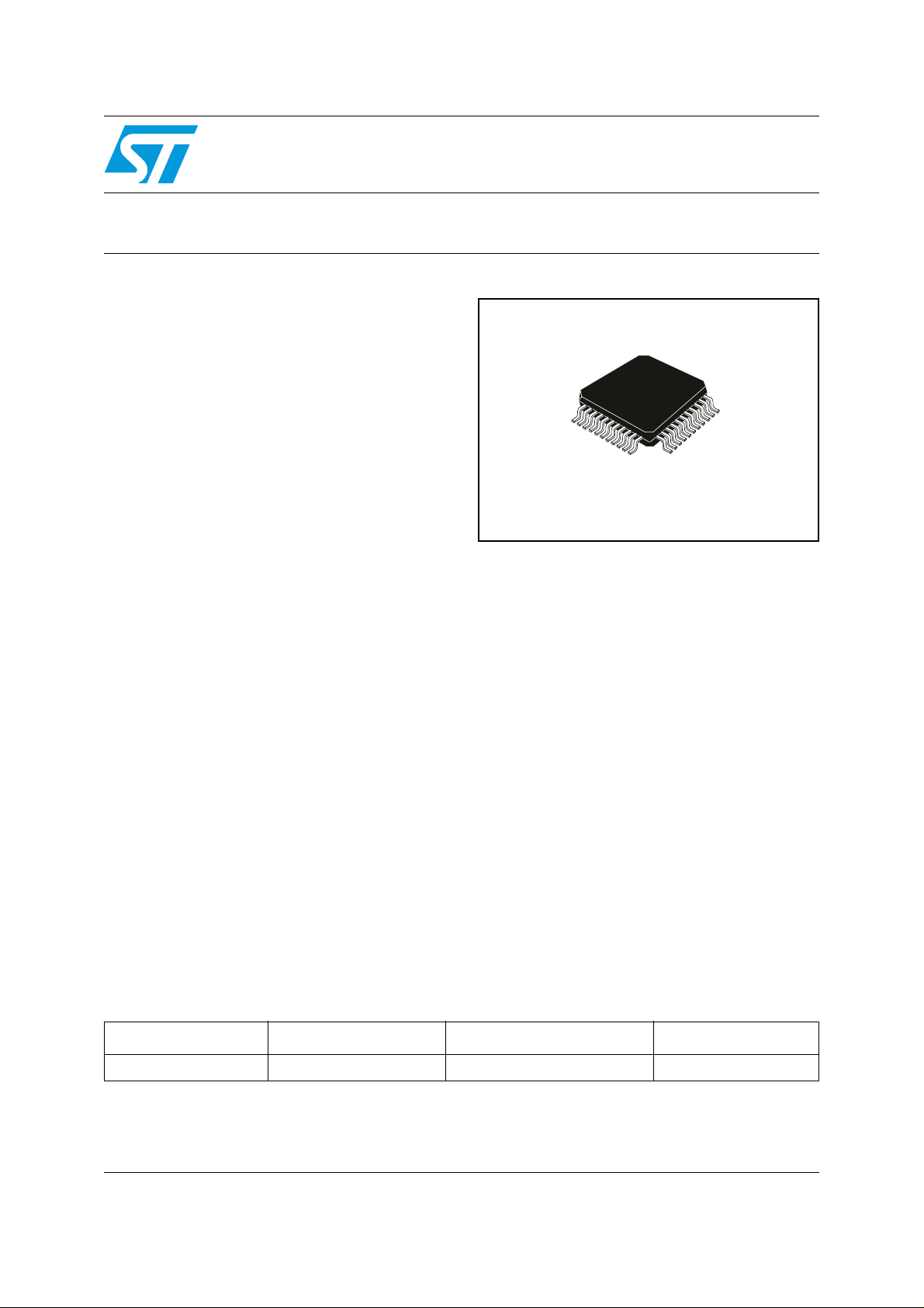
1/4 to 1/11-duty VFD controller/driver
General features
■ Many display modes (11 segments & 11 digits
to 16 segments & 4 digits)
■ Key scanning (6 x 4 matrix)
■ Dimming circuit (eight steps)
■ High-voltage output (V
■ LED ports (4 chs, 20mA max)
■ General purpose input port (4 bits)
■ No external resistor necessary for driver output
(P-channel open drain + pull down resistor
output)
■ Serial interface (CLK, STB, D
– 35V max)
DD
IN
, D
OUT
)
STM86312
PQFP44
Description
The STM86312 is a VFD (Vacuum Fluorescent
Display) controller/driver that is driven on a 1/4 to
1/11-duty factor . It consists of 1 1-segments output
lines, 6 grid output lines, 5 segments/grid output
drive lines, a display memory, a control circuit,
and a key scan circuit. Serial data are input to the
STM86312 through a three-line serial interface.
This VFD controller/driver is ideal as a peripheral
device for a single-chip microcomputer.
Order codes
Part number Temperature range Package Tube
STM86312 -40 to 85 °C PQFP44 Tray
March 2006 Rev 2 1/24
www.st.com
24
Page 2

Contents STM86312
Contents
1 Block diagram . . . . . . . . . . . . . . . . . . . . . . . . . . . . . . . . . . . . . . . . . . . . . . 3
2 Pin settings . . . . . . . . . . . . . . . . . . . . . . . . . . . . . . . . . . . . . . . . . . . . . . . . 4
2.1 Pin connection . . . . . . . . . . . . . . . . . . . . . . . . . . . . . . . . . . . . . . . . . . . . . . 4
2.2 Pin description . . . . . . . . . . . . . . . . . . . . . . . . . . . . . . . . . . . . . . . . . . . . . . 5
3 Maximum rating . . . . . . . . . . . . . . . . . . . . . . . . . . . . . . . . . . . . . . . . . . . . . 6
3.1 Thermal data . . . . . . . . . . . . . . . . . . . . . . . . . . . . . . . . . . . . . . . . . . . . . . . 6
3.2 Recommended operating conditions . . . . . . . . . . . . . . . . . . . . . . . . . . . . . 6
4 Electrical characteristics . . . . . . . . . . . . . . . . . . . . . . . . . . . . . . . . . . . . . 8
5 Display RAM address and display mode . . . . . . . . . . . . . . . . . . . . . . . 10
6 LED port . . . . . . . . . . . . . . . . . . . . . . . . . . . . . . . . . . . . . . . . . . . . . . . . . . 12
7 SW data . . . . . . . . . . . . . . . . . . . . . . . . . . . . . . . . . . . . . . . . . . . . . . . . . . 13
8 Commands . . . . . . . . . . . . . . . . . . . . . . . . . . . . . . . . . . . . . . . . . . . . . . . . 14
8.1 Display mode setting command . . . . . . . . . . . . . . . . . . . . . . . . . . . . . . . . 14
8.2 Data setting comma nd . . . . . . . . . . . . . . . . . . . . . . . . . . . . . . . . . . . . . . . 15
8.3 Address setting command . . . . . . . . . . . . . . . . . . . . . . . . . . . . . . . . . . . . 15
8.4 Display control com mand . . . . . . . . . . . . . . . . . . . . . . . . . . . . . . . . . . . . . 16
9 Serial communication format . . . . . . . . . . . . . . . . . . . . . . . . . . . . . . . . . 17
10 Application . . . . . . . . . . . . . . . . . . . . . . . . . . . . . . . . . . . . . . . . . . . . . . . . 19
11 Mechanical data . . . . . . . . . . . . . . . . . . . . . . . . . . . . . . . . . . . . . . . . . . . . 21
12 Revision history . . . . . . . . . . . . . . . . . . . . . . . . . . . . . . . . . . . . . . . . . . . 23
2/24
Page 3

STM86312 Block diagram
1 Block diagram
Figure 1. Block diagram
3/24
Page 4
Pin settings STM86312
2 Pin settings
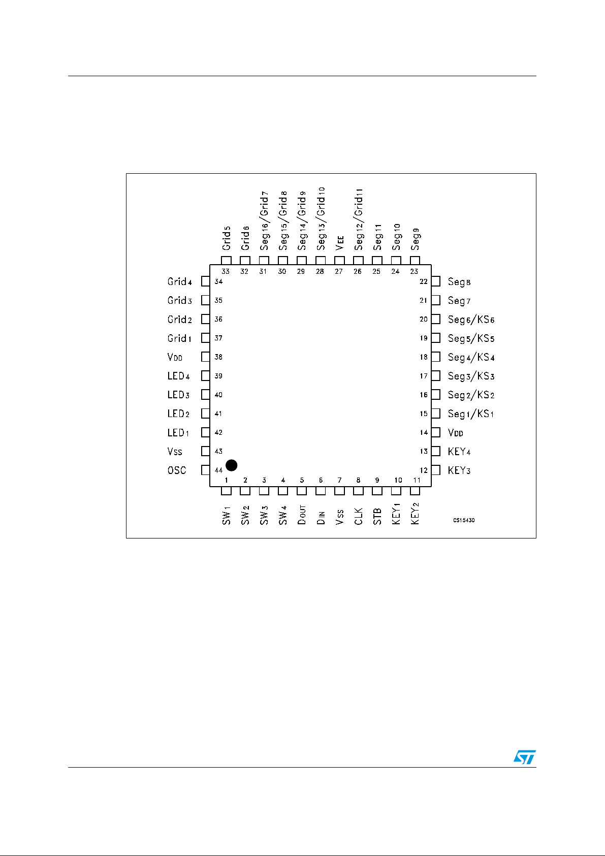
2.1 Pin connection
Figure 2. Pin connection
4/24
Page 5
STM86312 Pin se tt i ngs
2.2 Pin description
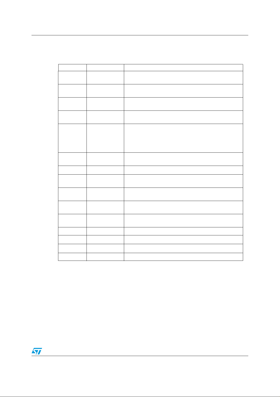
Table 1. Pin description
Pin N° Symbol Name and function
1, 2, 3, 4
SW1, SW2,
SW3, SW4
General-purpose switch inputs.
5
6
D
OUT
D
IN
8CLK
9STB
10, 11, 12, 13
14, 38
15, 16, 17,
18, 19, 20
21, 22, 23,
24, 25
26, 28, 29,
30, 31
32, 33, 34,
35, 36, 37
KEY1, KEY2,
KEY3, KEY4
V
DD
SEG1/KS1 to
SEG6/KS6
SEG7 to SEG11 Segment output pins.
SEG12/GRID11 to
SEG16/GRID7
GRID1 to GRID 6 Grid output pins.
Output serial data at falling edge of the shift clock, starting
from lower bit. This is N-ch open-drain output pin.
Input serial data at rising edge of the shift clock, starting from
lower bit.
Reads serial dat a at rising edge, and outputs data at falling
edge.
Initializes serial interface at risi ng or falling edge to make
STM86312 waiting f or reception of command. Data input after
STB has fall en are pr ocessed as a command. Whi le co mmand
data are processed, current processing is sto pped, and the
serial interfac e is initi alize d. While STB is high, CLK is ignored.
Input data to these pins are latched at end of the display cycle.
5V ± 10%.
Segment output pin s (Dual function as key source).
These pins are selectable for segment or grid driving.
39, 40, 41, 42 LED1 to LED4 CMOS outputs. +20 mA max.
7, 43
27
V
SS
V
EE
Connect this pin to system GND.
Pull-dow n le vel . V
- 35V max .
DD
44 OSC Connect to an external resistor.
5/24
Page 6

Maximum rating STM86312
3 Maximum rating
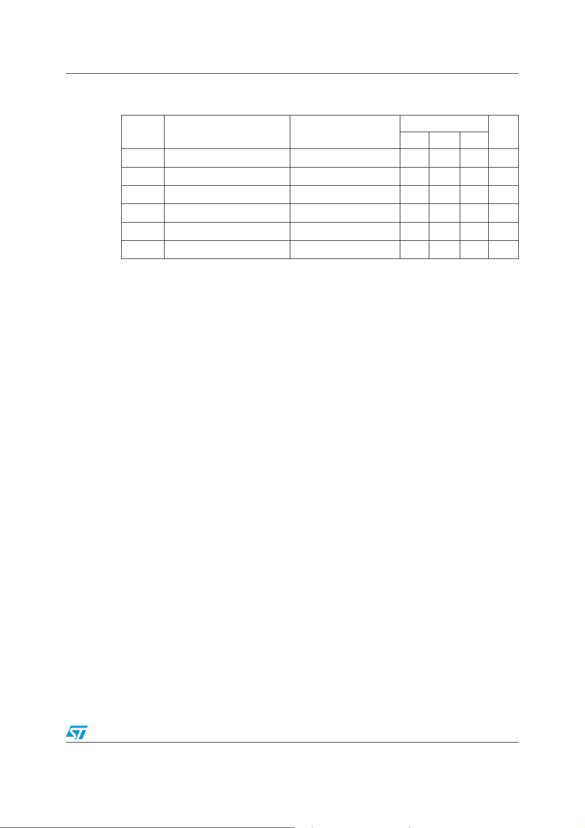
Stressing the device above the rating listed in the “Absolute Max imum Ratings” table may
cause permanent damage to the device. These are stress ratings only and operation of the
device at these or any other conditions above those indicated in the Operating sections of
this specification is not implied. Exposure to Absolute Maximum Rating conditions for
extended periods may affect device reliability. Refer also to the STMicroelectronics SURE
Program and other relevant quality documents.
Table 2. Absolute maximum rati ngs
Symbol Parameter Value Unit
V
V
V
I
I
Logic Supply Voltage -0.5 to 7 V
DD
Driver Supply Voltage
EE
V
Logic Input Voltage
I
VFD Driver Output Voltage
O2
LED Driver Output Current 25 mA
O1
VFD Driver Output Current
O2
T
Operating Ambient Temperature -40 to 85 °C
A
3.1 Thermal data
Table 3. Therma l data
Symbol Parameter Value Unit
R
thJC
Thermal Resistance Junction-case 56 °C/W
3.2 Recommended operating conditions
V
+0.5 to VDD-40
DD
-0.5 to V
-0.5 to VDD+0.5
V
EE
-40 (Grid)
-15 (Segment)
DD
+0.5
V
V
V
mA
Table 4. Recommended operating conditions
Symbol Parameter Min Typ Max Unit
V
DD
V
IH
V
IL
V
EE
6/24
Logic Supply Voltage 4.5 5 5.5 V
High Level Input Voltage 0.7xV
Low Level Input Voltage 0 0.3xV
Driver Supply Voltage 0 VDD-35 V
DD
V
DD
DD
V
V
Page 7

STM86312 Maximum rating
Maximum power consumption P
= VFD driver dissipation + RL dissipation + LED driver
MAX
dissipation + dynamic power consumption.
Where segment current = 3 mA, grid current = 15 mA, and LED current = 20 mA,
VFD driver dissipation = number of segments x 6 + number of grids/(number of grids + 1) x
30 (mW)
dissipation = (VDD - VEE)2/50 x (segment + 1) (mW)
R
L
LED driver dissipation = number of LEDs x 20 (mW)
Dynamic power consumption = V
x 5 (mW)
DD
Example
Where V
= -25 V, V
EE
= 5 V, and in 16-segment and 6-digit modes,
DD
VFD driver dissipation = 16 x 6 + 6/7 x 30 = 122
dissipation = 302/50 x 17 = 306
R
L
LED driver dissipation = 4 x 20 = 80
Dynamic power consumption = 5 x 5 = 25
Total 553 mW.
7/24
Page 8

Electrical characteristics STM86312
4 Electrical characteristics
Table 5. Electrical characteristics (V
to 70°C, unless otherwise noted. Typical values are at T
Symbol Parameter Test Conditions
V
V
V
I
OH21
High Level Output Voltage LED1-LED4, I
OH1
Low Level Output Voltage LED1-LED4, I
OL1
Low Level Output Voltage D
OL2
High Level Output Current VO = V
= 4.5 to 5.5V, V
DD
, I
OUT
OL2
DD
Seg11
= 0V, V
SS
= 25°C)
A
EE
= V
DD
- 35V, TA = -20
Value
Min. Typ. Max.
=-1mA 0.9V
OH1
=20mA 1 V
OL1
DD
= 4mA 0.4 V
- 2V, Seg1 to
-3 mA
Unit
V
I
OH22
High Level Output Current VO = V
- 2V, Grid1 to
DD
Grid6,
Seg12/Grid11 to
Seg16/Grid7
I
OLEAK
Driver Leakage Current VO = V
R
Output Pull-Down
L
- 35V, driver off -10 µA
DD
Driver Output 50 1 00 150 kΩ
Resistor
I
V
V
V
HYS
I
DDdyn
Input Current VI = V
I
High Level Input Voltage 0.7V
IH
Low Level Input Voltage 0.3V
IL
Hysteresis Voltage CLK, DIN, STB 0.35 V
Dynamic Current
Under no load, display off 5 mA
DD
or V
SS
Consumption
Table 6. Switching characteristics (V
= 4.5 to 5.5V, VSS = 0V, V
DD
to 70°C, unless otherwise noted. Typical values are at T
Symbol Parameter Test Conditions
t
t
t
TZH1
t
TZH2
Propagation Delay CLK → D
PLZ
OUT
RL = 10 kΩ, CL = 15 pF
PZL
Rise Time CL = 300 pFSeg1 to Seg11 2 µs
Grid1 to Grid6,
Seg12/Grid11 to
Seg16/Grid7
= 25°C)
A
-15 mA
±1 µA
DD
V
V
DD
EE
= V
DD
- 35V, TA = -20
Value
Unit
Min. Typ. Max.
300 ns
100
0.5
t
THZ
f
MAX
Fall Time CL = 300 pF , Segn, Gridn 120 µs
Maximum Clock
Duty = 50% 1 MHz
Frequency
C
Inpu t C a pacita nce 15 pF
I
8/24
Page 9
STM86312 Electrical characteristics
Table 7. Timing Ch aracteristics (V
noted. Typical values are at T
= 25°C)
A
= 4.5 to 5.5V, TA = -20 to 70°C, unless otherwise
DD
Symbol Parameter Test Conditions
PW
PW
t
SETUP
t
HOLD
t
CLK-STB
t
WAIT
Clock Pulse Width 400 ns
CLK
Strobe Pulse Width 1 µs
STB
Data Setup Ti me 100 ns
Data Hold Ti me 100 ns
Clock-St robe Time CLK ↑→ STB↑ 1µs
Wait Time (Note 1) CLK ↑→ CLK↓ 1µs
Note: Refer to page Serial Communication Format.
Value
Unit
Min. Typ. Max.
9/24
Page 10
Display RAM address and display mode STM86312
5 Display RAM address and display mode
The display RAM stores the data transmitted from an external device to the STM86312
through the serial interface; addresses are as follows, in 8-bits unit:
RAM stores
Seg1 Seg4 Seg8 Seg12 Seg16
addresses
00 H
L
02 H
L
04 H
L
06 H
L
08 H
L
0A H
L
0C H
L
0E H
L
10 H
L
12 H
L
14 H
L
b0 b3 b4 b7
XX H
Note: "0" in memory means V
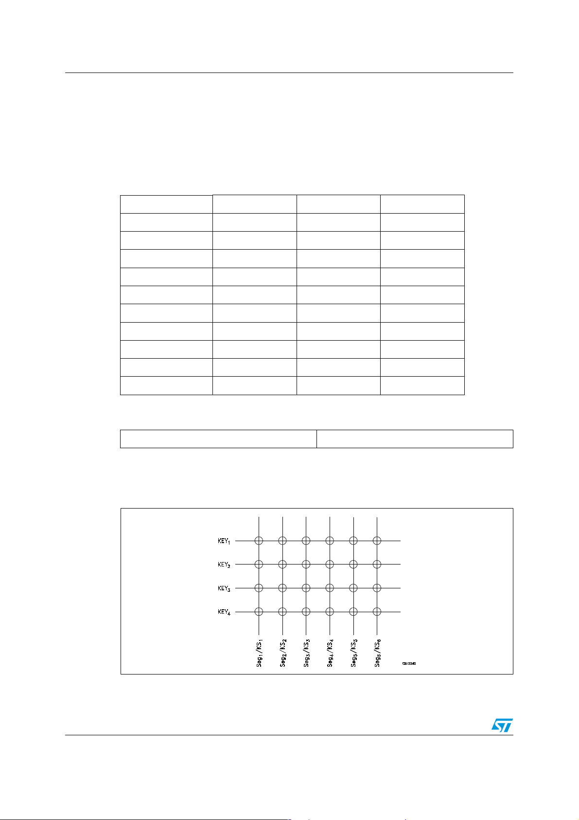
The key matrix is of 6 x 4 configuration, as shown below
00 H
U
02 H
U
04 H
U
06 H
U
08 H
U
0A H
U
0C H
U
0E H
U
10 H
U
12 H
U
14 H
U
L
on output; "1" in memory means VDD on output.
EE
01 H
03 H
05 H
07 H
09 H
0B H
0D H
0F H
11 H
13 H
15 H
L
L
L
L
L
L
L
L
L
L
L
0B H
0D H
XX H
01 H
03 H
05 H
07 H
09 H
0F H
11 H
13 H
15 H
U
U
U
U
U
U
U
U
U
U
U
U
DIG1
DIG2
DIG3
DIG4
DIG5
DIG6
DIG7
DIG8
DIG9
DIG10
DIG11
Figure 3. Ke y m at ri x and k ey-input data storage RAM
10/24
Page 11
STM86312 Display RAM address and di splay mode
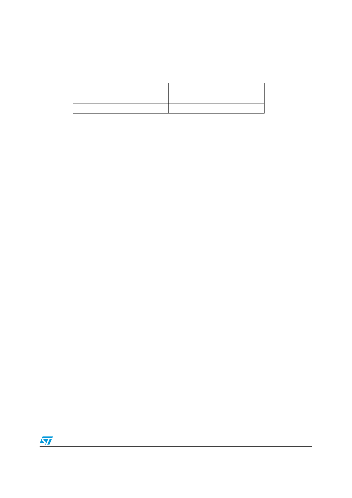
The data of each key are stored as illustrated below, and are read by the appropriate read
command, starting from the least significant bit
KEY1 KEY4 KEY1 KEY4
Seg1/KS1 Seg2/KS2 Ø
Seg3/KS3 Seg4KS4
Seg5/KS5 Seg6/KS6
b0 b3 b4 b7
11/24
Page 12
LED port STM86312
6 LED port
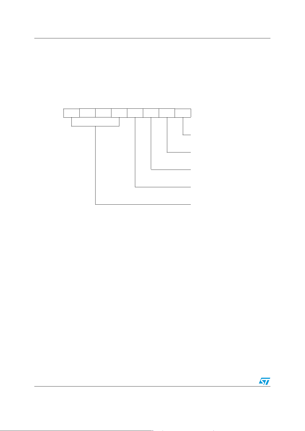
Data are written to the LED port by a write command, starting from the least significant bit of
the port. When a bit of this port is 0, the corresponding LED lights; when the bit is 1, the LED
goes off. The data of bits 5 through 8 are ignored.
Figure 4. LED port
MSB LSB
- - - - b3b2b1b0
LED1
LED2
LED3
On power application, all the LEDs remain dark.
LED4
Don’t Care
12/24
Page 13
STM86312 SW data
7 SW data
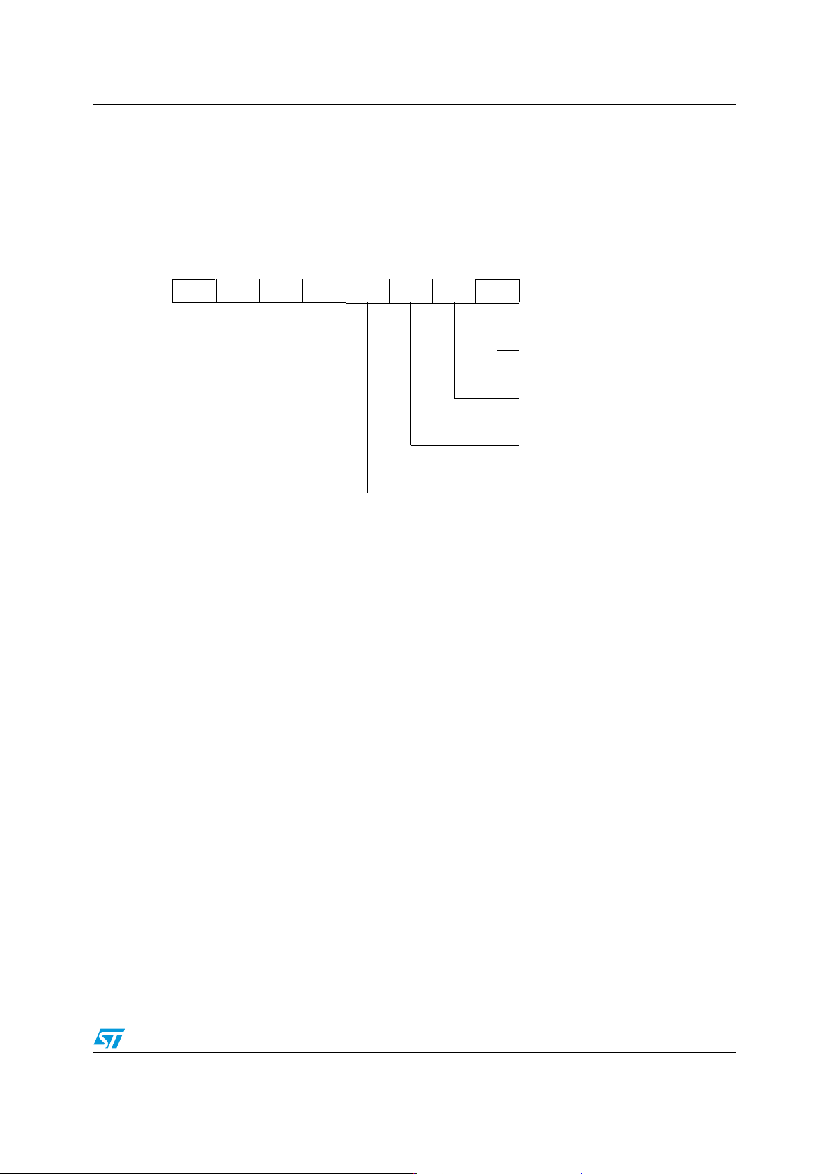
The SW data are read by the appropriate read command, starting from the least significant
bit. Bits 5 through 8 of the SW data are 0.
Figure 5. SW data
MSB LSB
0 0 0 0 b3 b2 b1 b0
SW1
SW2
SW3
SW4
13/24
Page 14
Commands STM86312
8 Commands
A command sets the display mode and status of the VFD driver.
The first 1 byte input to the STM86312 through the D
regarded as a command. If STB is set high while commands/data are transmitted, serial
communication is initialized, and the commands/data being transmitted are invalid
(however, the commands/data already transmitted remain valid).
8.1 Display mode setting command
This command initializes the STM86312 and selects the number of segments and number
of grids (1/4 to 1/11 duty, 11 segments to 16 segments).
When this command is executed, display is forcibly turned off, and key scanning is also
stopped. To resume display, the display ON command must be executed. If the same mode
is selected, however, nothing is performed.
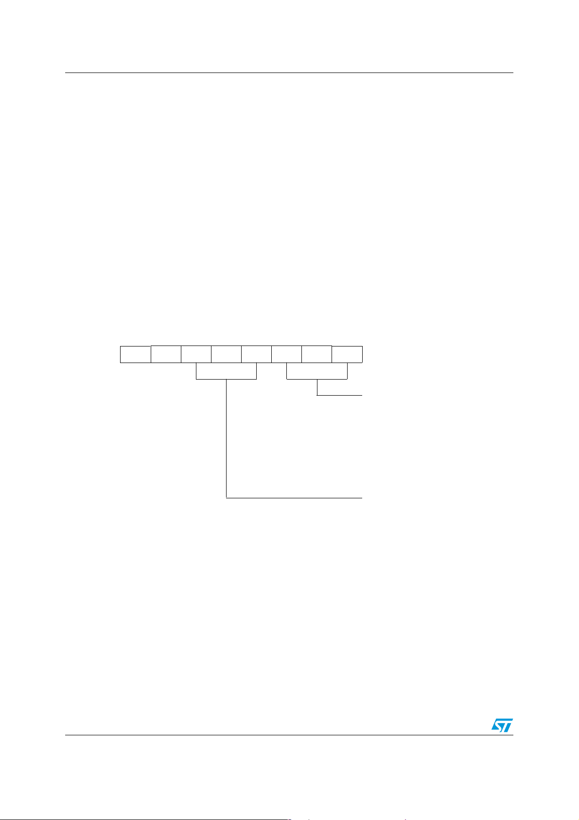
Figure 6. Display mode settings
MSB LSB
00- - -b2b1b0
pin after the STB pin has fallen is
IN
Display mode setti ng
000 : 4 digits, 16 segments
001 : 5 digits, 16 segments
010 : 6 digits, 16 segments
01 1 : 7 digits, 15 segments
100 : 8 digits, 14 segments
101 : 9 digits, 13 segments
110 : 10 digits, 12 segments
1 11 : 11 digits, 11 segments
On power application, the 11-digit 11-segment mode is selected.
14/24
Don’t Care
Page 15
STM86312 Commands
8.2 Data setting com mand
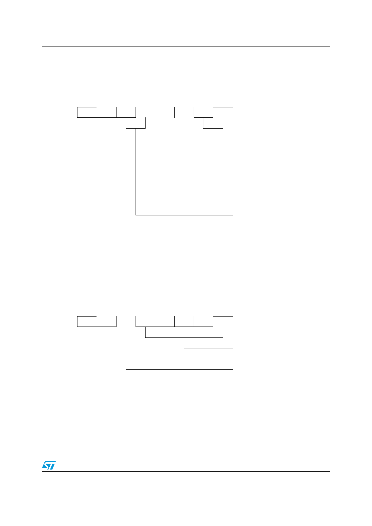
This command sets data write and data read modes.
Figure 7. Data setting command
MSB LSB
01- -0b2b1b0
Data write and read mode setting
00 : Write data to dis p la y memo ry
01 : Write data to LED port
10 : Read key data
11 : Read SW data
ADDRESS INCREMENT MODE
SETTING (DISPLAY MEMORY)
0= Increments addr ess af ter d at a has
been written
1= Fixed address
Don’t Care
On power application, the normal operation mode and address increment mode are set.
Do not use STM86312 in test mode.
8.3 Address setting command
This command sets an address of the display memory
Figure 8. Address setting command
MSB LSB
1 1 - b4b3b2b1b0
If address 16H or higher is set, the data are ignored, until a correct address is set.
On power application, the address is set to 00H.
Address (00H-15H)
Don’t Care
15/24
Page 16
Commands STM86312
8.4 Display control command
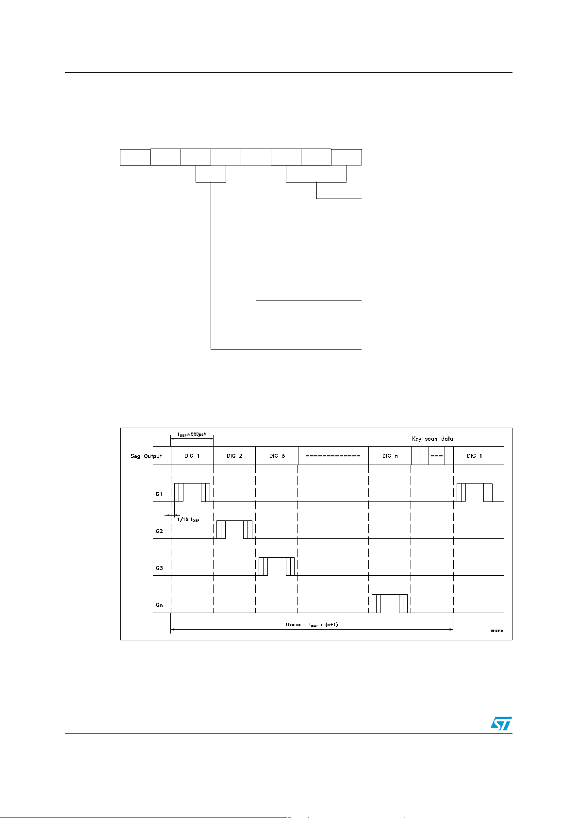
Figure 9. Display control command
MSB LSB
1 0 - - b3 b2 b1 b0
Display mode setti ng
000 : Set Pulse Width to 1/1 6
001 : Set Pulse Width to 2/1 6
010 : Set Pulse Width to 4/1 6
011 : Set Pulse Width to 10 /16
100 : Set Pulse Width to 11/16
101 : Set Pulse Width to 12/16
110 : Set Pulse Width to 13 /16
1 11 : Set Pulse Width to 14/16
TURNS ON/OFF DISPLAY
0= Display OFF
(Key Scan Continues note)
1= Display ON
Don’t Care
On power application, the 1/16-pulse width is set and the display is turned off.
Note: On power application, key scanning is stopped.
Figure 10. K ey scan ning and display timing
Note: * The value can be modified by trimmering R
OSC
One cycle of key scanning consists of one frame, and data of 6 x 4 matrices are stored in
RAM.
.
16/24
Page 17
STM86312 Serial communication format
9 Serial communication format
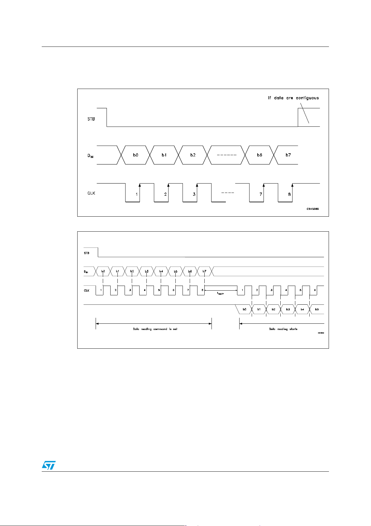
Figure 11. R ecep tion (comman d/da ta write)
Figure 12. Transmission (data read)
Because the D
up resistor to this pin (1 kΩ to 10 kΩ).
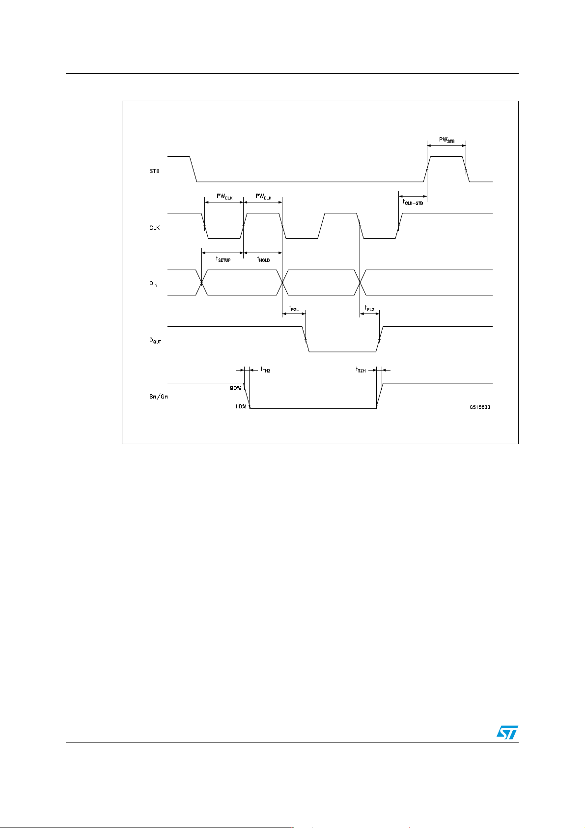
Note: *: When data are read, a wait time t
eighth clock that has set the command and the falling one of the first clock that has read the
data.
pin is an N-ch open-drain output pin, be sure to connect an external pull-
OUT
of 1µs is necessary within the rising edge of the
WAIT
17/24
Page 18
Serial communication format STM86312
Figure 13. Switching characteristics waveform
18/24
Page 19
STM86312 Application
10 Application
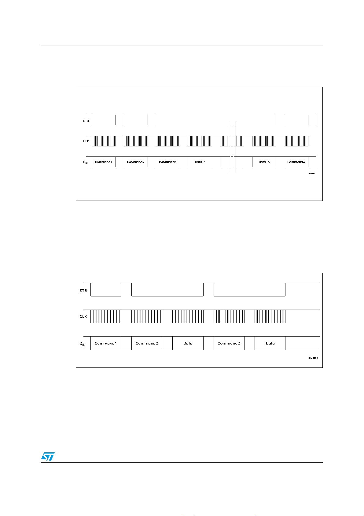
Figure 14. Updating display memory by incrementing address
Command 1: sets display mode
Command 2: sets data
Command 3: sets address
Data 1 to n: transfers display data (22 bytes max.)
Command 4: controls display
Figure 15. Updating specific address
Command 1: sets data
Command 2: sets address
Data: di s p lay data
19/24
Page 20
Application STM86312
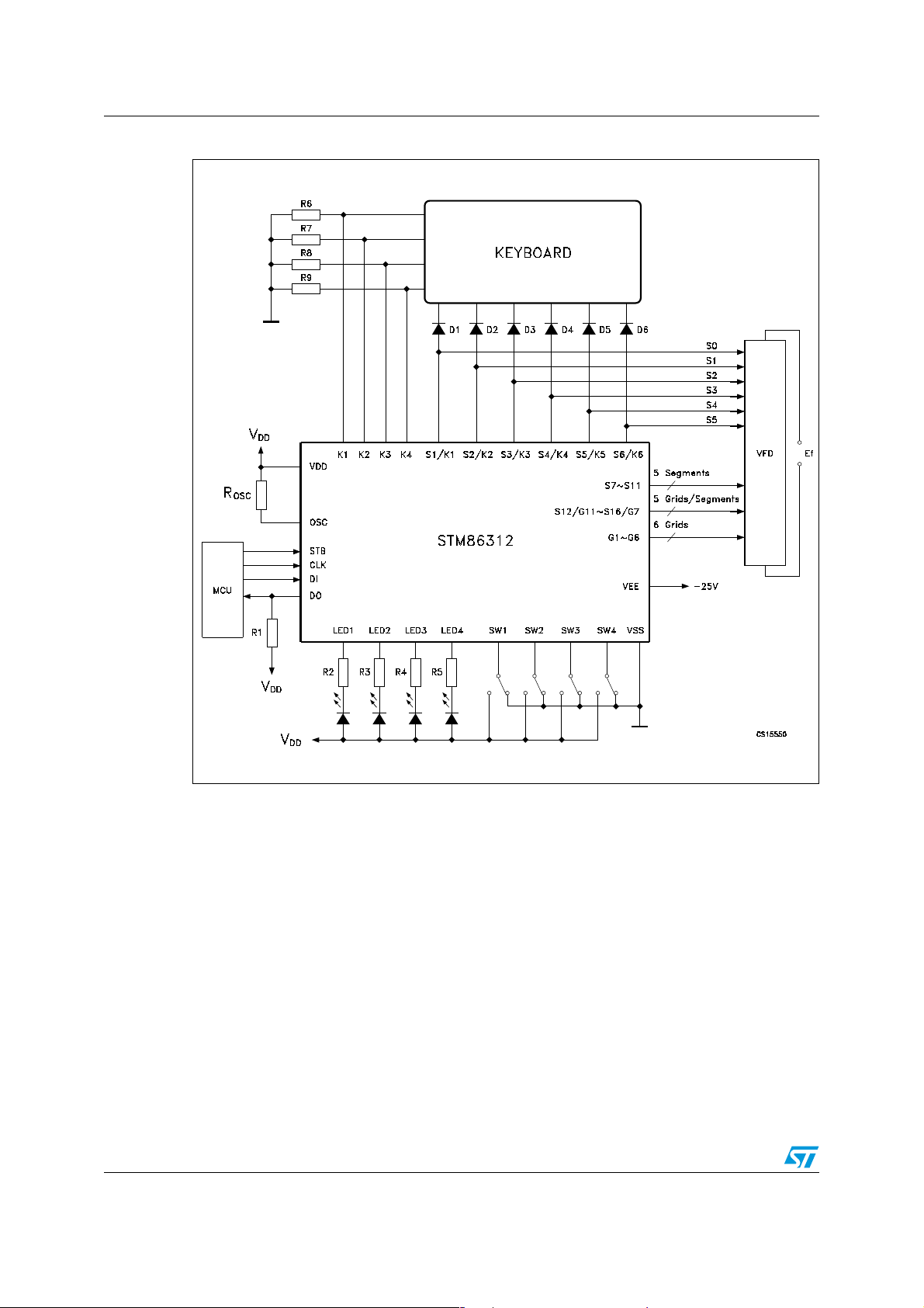
Figure 16. Application circuit
Note: R
1 R1=1~10 k
2 R2~R5 = 750
= 47kΩ for oscilla tor r es is tor
OSC
Ω
for external pull-high resistor
Ω
~1.2 k
Ω
3 R6~R9 = 10kΩ for external pull-low resistor
4 D1~D6 = 1N4001
5 Ef = Filament voltage for VFD.
20/24
Page 21

STM86312 Mecha nical data
11 Mechanical data
In order to meet environmental requirements, ST offers these devices in ECOPACK®
packages. These packages have a Lead-free second level interconnect . The category of
second level interconnect is marked on the package and on the inner box label, in
compliance with JEDEC Standard JESD97. The maximum ratings related to soldering
conditions are also marked on the inner box label. ECOPACK is an ST trademark.
ECOPACK spec ifications are available at: www.st.com
21/24
Page 22
Mechanical data STM86312
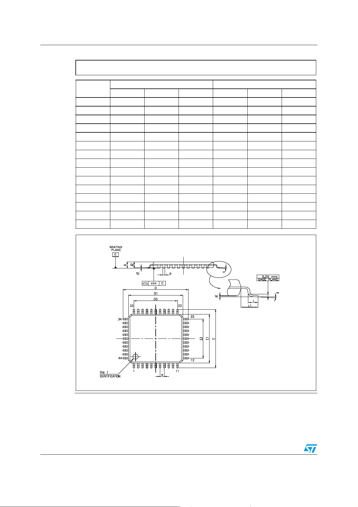
PQFP44 MECHANICAL DATA
DIM.
MIN. TYP MAX. MIN. TYP. MAX.
mm. inch
A 2.45 0.096
A1 0.25 0.010
A2 1.80 2.00 2.20 0.071 0.079 0.087
b 0.29 0.45 0.011 0.018
c 0.11 0.23 0.004 0.009
D 13.2 0.520
D1 10.00 0.394
D3 8.00 0.315
E 13.2 0.520
E1 10.00 0.394
E3 8.00 0.315
e 0.80 0.031
L 0.73 0.88 1.03 0.029 0.035 0.041
L1 1.6 0.063
K 0°3.5°7° 0°3.5°7°
22/24
0076922/D
Page 23
STM86312 Revision history
12 Revision history
Table 8. Revision history
Date Revision Changes
27-May-2004 1 First Release
27-Mar-2006 2 New Temp, few changes
23/24
Page 24

STM86312
I
e
r
y
t
A
P
o
l
N
is
d
ts
o
h
t
U
D
W
D
W
S
O
U
D,
A
S,
N
R
S
R
id
a
y
l
Please Read Caref u ll y:
nformation in this document is provided solely in connection with ST products. STMicroelectronics NV and its subsidiaries (“ST”) reserve th
ight to make changes, corrections, modifications or improvements, to this document, and the products and services described herein at an
ime, without notice.
ll ST product s are sold pursuant to ST’ s te rm s and condit io ns of sale.
urchasers are solely responsible for the choice, selection and use of the ST products and servi ces descri bed herein , and ST ass um es n
iability whatsoever relating to the choice, selection or use of the ST products and services described herein.
o license, express or implied, by estoppel or otherwise, to any intellectual property rights is granted under this document. If any part of th
ocument refers to any third par ty products or services i t s hall not be d eem ed a licen se grant by ST f or the use of such third party produc
r services , or any intel lec tual pro per ty cont aine d ther ein or con sidere d as a warra nty c overi ng th e use i n any mann er w hats oever of suc
hird part y products or services or any intellectual property contained therein.
NLESS OTHERWISE SET FORTH IN ST’S TERMS AND CONDITIONS OF SALE ST DISCLAIMS ANY EXPRESS OR IMPLIE
ARRANTY WITH RESPECT TO THE USE AND/OR SALE OF ST PRODUCTS INCLUDING WITHOUT LIMITATION IMPLIE
ARRANTIES OF MERCHANTABILITY, FITNESS FOR A PARTICULAR PURPOSE (AND THEIR EQUIVALENTS UNDER THE LAW
F ANY JURISDICTION), OR INFRINGEMENT OF ANY PATENT, COPYRIGHT OR OTHER INTELLECTUAL PROPERTY RIGHT.
NLESS EXPRESSLY APPROVED IN WRI TING BY A N AUTH ORIZE REP RESENTATI VE OF S T, ST PRODUCTS ARE NOT DESIGNE
UTHORIZ ED OR WARRANT ED FOR USE IN MI L IT A RY, AIR CRAF T , S PACE, LIFE SAV ING, OR LIFE SUSTAINING APPLICATION
OR IN PRODUCTS OR SYSTEMS, WHERE FAILURE OR MALFUNCTION MAY RESULT IN PERSONAL INJURY, DEATH, O
EVERE PROPERTY OR ENVIRONMENTAL DAMAGE.
esale of ST products with provisions different from the statements and/or technical features set forth in this document shall immediately vo
ny warran ty gr anted by ST fo r the ST produc t or se rvice d es cribed he rein and shall not c reat e o r extend in a ny mann er wha tsoe ve r, an
iability of ST.
The ST logo is a registered trademark of STMicroelectronics. All other names are the property of their respective owners.
ST and the ST logo are trademarks or regis t ered trademarks of ST in vari ous countri es.
Information in this docum ent supersedes and replaces all information pr eviously sup pl i ed.
© 2006 STMi croelectro n ics - All rights reserved
Austra l i a - Be l gi um - Brazil - Canada - China - Czech Rep ubl i c - Finland - F rance - Germany - Hong Kon g - In di a - Israel - It al y - Japan -
STMicroelectron ics group of com panies
Malaysi a - M al ta - Morocco - Singapore - Spain - Sweden - Switze rl and - Unite d Kingdom - Unit ed States of America
www.st.com
24/24
 Loading...