

Features
■ 5 V operating voltage
■ Precision V
– STM705/707/813L
–4.50 V
– STM706/708
–4.25
■ RST and RST outputs
■ 200 ms (typ) t
■ Watchdog timer - 1.6 s (typ)
■ Manual reset input (MR)
■ Power-fail comparator (PFI/PFO)
■ Low supply current - 40 µA (typ)
■ Guaranteed RST (RST) assertion down to
V
= 1.0 V
CC
■ Operating temperature: –40 °C to 85 °C
(industrial grade)
■ RoHS compliance
– Lead-free components are compliant with
the RoHS directive
≤
CC
≤
V
monitor
V
≤
RST
≤
RST
rec
4.75 V
4.50 V
STM705, STM706
STM707, STM708, STM813L
5 V supervisor
8
1
SO8 (M)
TSSOP8 3x3 (DS)
1. Contact local ST sales office for availability.
(1)
Table 1. Device summary
Watchdog
input
STM705 ✓✓✓ ✓ ✓
STM706 ✓✓✓ ✓ ✓
STM707 ✓✓ ✓ ✓
STM708 ✓✓ ✓ ✓
STM813L ✓✓ ✓✓ ✓
1. Push-pull output
August 2010 Doc ID 10520 Rev 9 1/33
Watchdog
output
(1)
Active-low
(1)
RST
Active-high
(1)
RST
Manual reset
input
Power-fail
comparator
www.st.com
1

Contents STM705, STM706, STM707, STM708, STM813L
Contents
1 Description . . . . . . . . . . . . . . . . . . . . . . . . . . . . . . . . . . . . . . . . . . . . . . . . . 5
2 Pin descriptions . . . . . . . . . . . . . . . . . . . . . . . . . . . . . . . . . . . . . . . . . . . . 8
2.1 MR . . . . . . . . . . . . . . . . . . . . . . . . . . . . . . . . . . . . . . . . . . . . . . . . . . . . . . . 8
2.2 WDI . . . . . . . . . . . . . . . . . . . . . . . . . . . . . . . . . . . . . . . . . . . . . . . . . . . . . . 8
2.3 WDO
2.4 RST
2.5 RST . . . . . . . . . . . . . . . . . . . . . . . . . . . . . . . . . . . . . . . . . . . . . . . . . . . . . . 8
2.6 PFI . . . . . . . . . . . . . . . . . . . . . . . . . . . . . . . . . . . . . . . . . . . . . . . . . . . . . . . 8
2.7 PFO
. . . . . . . . . . . . . . . . . . . . . . . . . . . . . . . . . . . . . . . . . . . . . . . . . . . . . . 8
. . . . . . . . . . . . . . . . . . . . . . . . . . . . . . . . . . . . . . . . . . . . . . . . . . . . . . 8
. . . . . . . . . . . . . . . . . . . . . . . . . . . . . . . . . . . . . . . . . . . . . . . . . . . . . . 9
3 Operation . . . . . . . . . . . . . . . . . . . . . . . . . . . . . . . . . . . . . . . . . . . . . . . . . 11
3.1 Reset output . . . . . . . . . . . . . . . . . . . . . . . . . . . . . . . . . . . . . . . . . . . . . . . 11
3.2 Push-button reset input . . . . . . . . . . . . . . . . . . . . . . . . . . . . . . . . . . . . . . 11
3.3 Watchdog input (STM705/706/813L) . . . . . . . . . . . . . . . . . . . . . . . . . . . . 11
3.4 Watchdog output (STM705/706/813L) . . . . . . . . . . . . . . . . . . . . . . . . . . . 12
3.5 Power-fail input/output . . . . . . . . . . . . . . . . . . . . . . . . . . . . . . . . . . . . . . . 12
3.6 Ensuring a valid reset output down to V
3.7 Interfacing to microprocessors with bidirectional reset pins . . . . . . . . . . . 13
= 0 V . . . . . . . . . . . . . . . . . . . 12
CC
4 Typical operating characteristics . . . . . . . . . . . . . . . . . . . . . . . . . . . . . 14
5 Maximum ratings . . . . . . . . . . . . . . . . . . . . . . . . . . . . . . . . . . . . . . . . . . . 22
6 DC and AC parameters . . . . . . . . . . . . . . . . . . . . . . . . . . . . . . . . . . . . . . 23
7 Package mechanical data . . . . . . . . . . . . . . . . . . . . . . . . . . . . . . . . . . . . 27
8 Part numbering . . . . . . . . . . . . . . . . . . . . . . . . . . . . . . . . . . . . . . . . . . . . 30
9 Revision history . . . . . . . . . . . . . . . . . . . . . . . . . . . . . . . . . . . . . . . . . . . 31
2/33 Doc ID 10520 Rev 9

STM705, STM706, STM707, STM708, STM813L List of tables
List of tables
Table 1. Device summary . . . . . . . . . . . . . . . . . . . . . . . . . . . . . . . . . . . . . . . . . . . . . . . . . . . . . . . . . . 1
Table 2. Signal names . . . . . . . . . . . . . . . . . . . . . . . . . . . . . . . . . . . . . . . . . . . . . . . . . . . . . . . . . . . . 6
Table 3. Pin description . . . . . . . . . . . . . . . . . . . . . . . . . . . . . . . . . . . . . . . . . . . . . . . . . . . . . . . . . . . 9
Table 4. Absolute maximum ratings . . . . . . . . . . . . . . . . . . . . . . . . . . . . . . . . . . . . . . . . . . . . . . . . . 22
Table 5. Operating and AC measurement conditions. . . . . . . . . . . . . . . . . . . . . . . . . . . . . . . . . . . . 23
Table 6. DC and AC characteristics . . . . . . . . . . . . . . . . . . . . . . . . . . . . . . . . . . . . . . . . . . . . . . . . . 25
Table 7. SO8 - 8-lead plastic small outline, 150 mils body width, pack. mech. data . . . . . . . . . . . . 28
Table 8. TSSOP8 - 8-lead, thin shrink small outline, 3 x 3 mm body size, mechanical data . . . . . . 29
Table 9. Ordering information scheme . . . . . . . . . . . . . . . . . . . . . . . . . . . . . . . . . . . . . . . . . . . . . . . 30
Table 10. Marking description. . . . . . . . . . . . . . . . . . . . . . . . . . . . . . . . . . . . . . . . . . . . . . . . . . . . . . . 30
Table 11. Document revision history . . . . . . . . . . . . . . . . . . . . . . . . . . . . . . . . . . . . . . . . . . . . . . . . . 31
Doc ID 10520 Rev 9 3/33

List of figures STM705, STM706, STM707, STM708, STM813L
List of figures
Figure 1. Logic diagram (STM705/706/813L) . . . . . . . . . . . . . . . . . . . . . . . . . . . . . . . . . . . . . . . . . . . 5
Figure 2. Logic diagram (STM707/708) . . . . . . . . . . . . . . . . . . . . . . . . . . . . . . . . . . . . . . . . . . . . . . . . 5
Figure 3. STM705/706/813L SO8 connections . . . . . . . . . . . . . . . . . . . . . . . . . . . . . . . . . . . . . . . . . . 6
Figure 4. STM705/706/813L TSSOP8 connections . . . . . . . . . . . . . . . . . . . . . . . . . . . . . . . . . . . . . . 6
Figure 5. STM707/708 SO8 connections . . . . . . . . . . . . . . . . . . . . . . . . . . . . . . . . . . . . . . . . . . . . . . 7
Figure 6. STM707/708 TSSOP8 connections . . . . . . . . . . . . . . . . . . . . . . . . . . . . . . . . . . . . . . . . . . . 7
Figure 7. Block diagram (STM705/706/813L) . . . . . . . . . . . . . . . . . . . . . . . . . . . . . . . . . . . . . . . . . . . 9
Figure 8. Block diagram (STM707/708) . . . . . . . . . . . . . . . . . . . . . . . . . . . . . . . . . . . . . . . . . . . . . . 10
Figure 9. Hardware hookup . . . . . . . . . . . . . . . . . . . . . . . . . . . . . . . . . . . . . . . . . . . . . . . . . . . . . . . . 10
Figure 10. Reset output valid to ground circuit . . . . . . . . . . . . . . . . . . . . . . . . . . . . . . . . . . . . . . . . . . 12
Figure 11. Interfacing to microprocessors with bidirectional reset I/O . . . . . . . . . . . . . . . . . . . . . . . . . 13
Figure 12. Supply current vs. temperature (no load) . . . . . . . . . . . . . . . . . . . . . . . . . . . . . . . . . . . . . . 14
Figure 13. V
Figure 14. Reset comparator propagation delay vs. temperature . . . . . . . . . . . . . . . . . . . . . . . . . . . . 15
Figure 15. Power-up t
Figure 16. Normalized reset threshold vs. temperature . . . . . . . . . . . . . . . . . . . . . . . . . . . . . . . . . . . . 16
Figure 17. Watchdog time-out period vs. temperature . . . . . . . . . . . . . . . . . . . . . . . . . . . . . . . . . . . . 16
Figure 18. PFI to PFO
Figure 19. Output voltage vs. load current (V
Figure 20. RST
Figure 21. RST output voltage vs. supply voltage . . . . . . . . . . . . . . . . . . . . . . . . . . . . . . . . . . . . . . . . 18
Figure 22. RST
Figure 23. RST response time (assertion) . . . . . . . . . . . . . . . . . . . . . . . . . . . . . . . . . . . . . . . . . . . . . 20
Figure 24. Power-fail comparator response time (assertion) . . . . . . . . . . . . . . . . . . . . . . . . . . . . . . . . 20
Figure 25. Power-fail comparator response time (de-assertion) . . . . . . . . . . . . . . . . . . . . . . . . . . . . . 21
Figure 26. Maximum transient duration vs. reset threshold overdrive . . . . . . . . . . . . . . . . . . . . . . . . . 21
Figure 27. AC testing input/output waveforms . . . . . . . . . . . . . . . . . . . . . . . . . . . . . . . . . . . . . . . . . . . 23
Figure 28. Power-fail comparator waveform . . . . . . . . . . . . . . . . . . . . . . . . . . . . . . . . . . . . . . . . . . . . 23
Figure 29. MR
Figure 30. Watchdog timing (STM705/706/813L) . . . . . . . . . . . . . . . . . . . . . . . . . . . . . . . . . . . . . . . . 24
Figure 31. SO8 – 8-lead plastic small outline, 150 mils body width, outline . . . . . . . . . . . . . . . . . . . . 28
Figure 32. TSSOP8 – 8-lead, thin shrink small outline, 3 x 3 mm body size, outline . . . . . . . . . . . . . 29
threshold vs. temperature . . . . . . . . . . . . . . . . . . . . . . . . . . . . . . . . . . . . . . . . . . . . . . 14
PFI
vs. temperature . . . . . . . . . . . . . . . . . . . . . . . . . . . . . . . . . . . . . . . . . . . . . . 15
rec
propagation delay vs. temperature . . . . . . . . . . . . . . . . . . . . . . . . . . . . . . . . . 17
= 5 V; TA = 25 °C) . . . . . . . . . . . . . . . . . . . . . . . . . . 17
output voltage vs. supply voltage . . . . . . . . . . . . . . . . . . . . . . . . . . . . . . . . . . . . . . . 18
response time (assertion) . . . . . . . . . . . . . . . . . . . . . . . . . . . . . . . . . . . . . . . . . . . . . 19
timing waveform . . . . . . . . . . . . . . . . . . . . . . . . . . . . . . . . . . . . . . . . . . . . . . . . . . . . . . 24
CC
4/33 Doc ID 10520 Rev 9
STM705, STM706, STM707, STM708, STM813L Description
1 Description
The STM705/706/707/708/813L supervisors are self-contained devices which provide
microprocessor supervisory functions. A precision voltage reference and comparator
monitors the V
occurs, the reset output (RST
These devices also offer a watchdog timer (except for STM707/708) as well as a power-fail
comparator to provide the system with an early warning of impending power failure.
These devices are available in a standard 8-pin SOIC package or a space-saving 8-pin
TSSOP package.
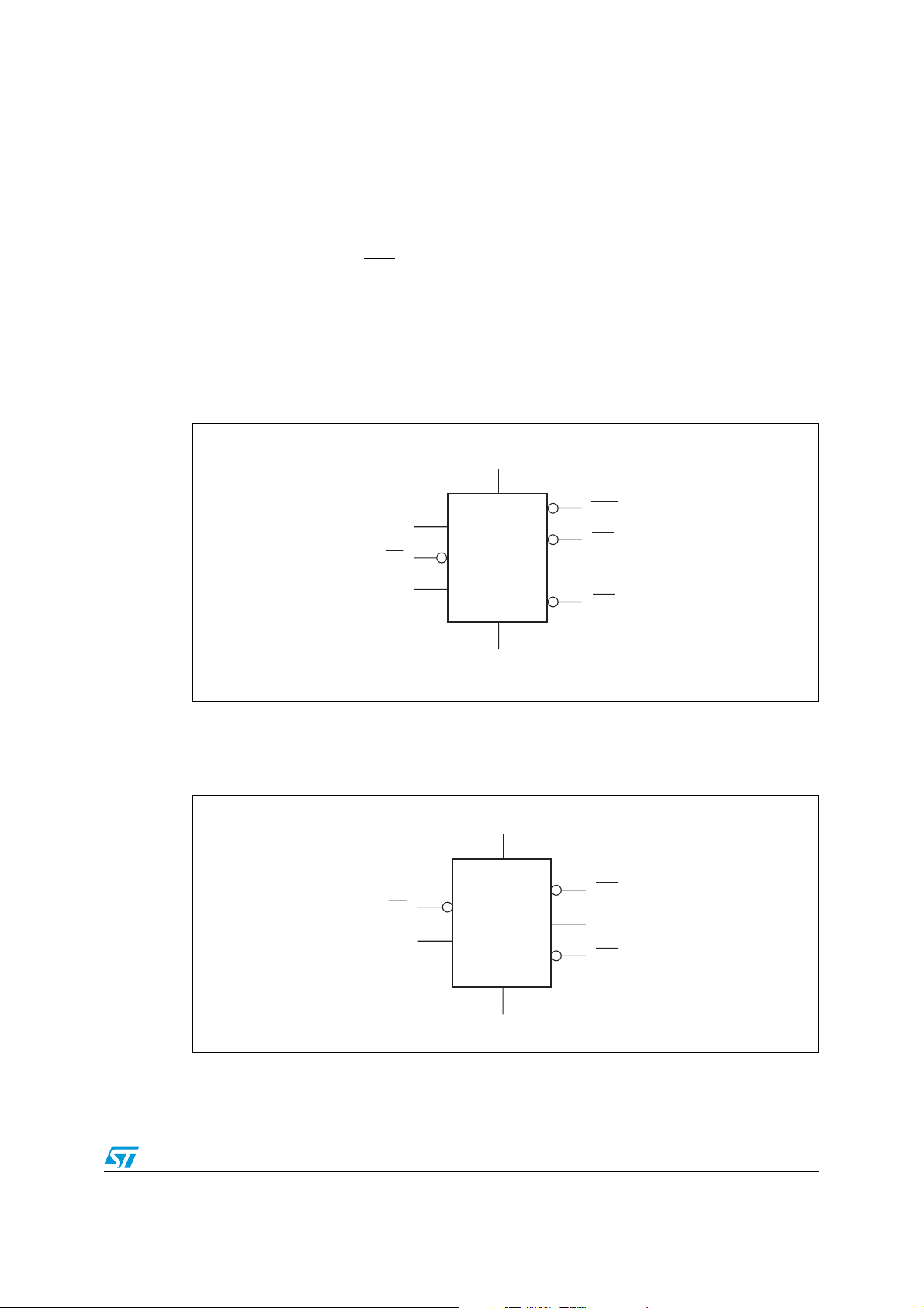
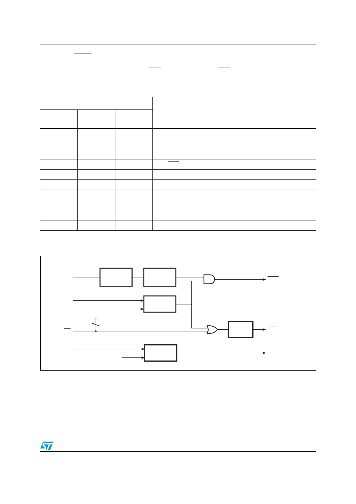
Figure 1. Logic diagram (STM705/706/813L)
input for an out-of-tolerance condition. When an invalid VCC condition
CC
) is forced low (or high in the case of RST).
V
CC
WDO
WDI
MR
PFI
STM705/706;
STM813L
RST
RST
PFO
(1)
(2)
1. For STM705/706 only.
2. For STM813L only.
Figure 2. Logic diagram (STM707/708)
MR
STM707/708
PFI
V
SS
AI08825
V
CC
RST
RST
PFO
V
SS
AI08826
Doc ID 10520 Rev 9 5/33
Description STM705, STM706, STM707, STM708, STM813L
Table 2. Signal names
MR Push-button reset input
WDI Watchdog input
Watchdog output
WDO
RST
Active-low reset output
(1)
RST
Supply voltage
V
CC
Active-high reset output
PFI Power-fail input
PFO Power-fail output
Ground
V
SS
NC No connect
1. For STM813L only.
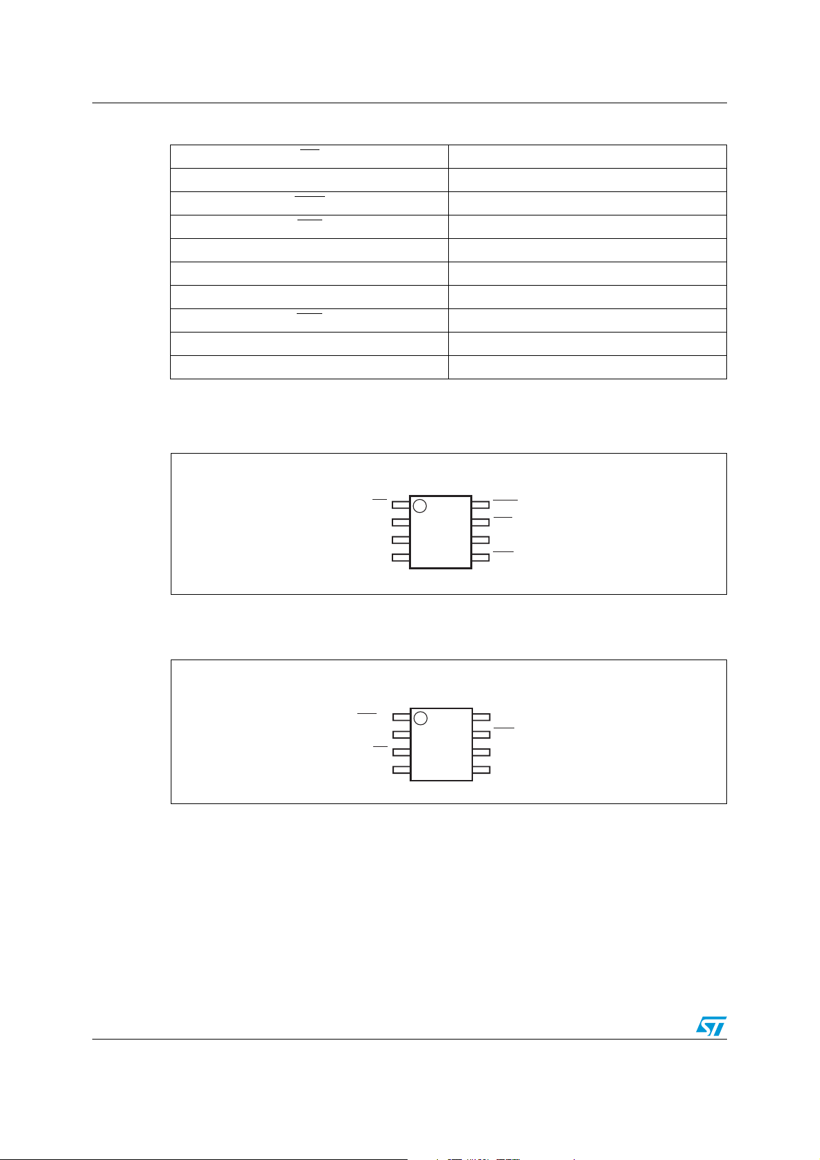
Figure 3. STM705/706/813L SO8 connections
SO8
MR
V
CC
V
SS
PFI
1
2
3
4
8
7
6
5
WDO
RST (RST)
WDI
PFO
1. For STM813L, reset output is active-high.
Figure 4. STM705/706/813L TSSOP8 connections
TSSOP8
WDO
MR
V
(1)
CC
(RST) RST
1. For STM813L, reset output is active-high.
1
2
3
4
WDI
8
PFO
7
PFI
6
V
5
(1)
AI08827a
SS
AI09114
6/33 Doc ID 10520 Rev 9
STM705, STM706, STM707, STM708, STM813L Description
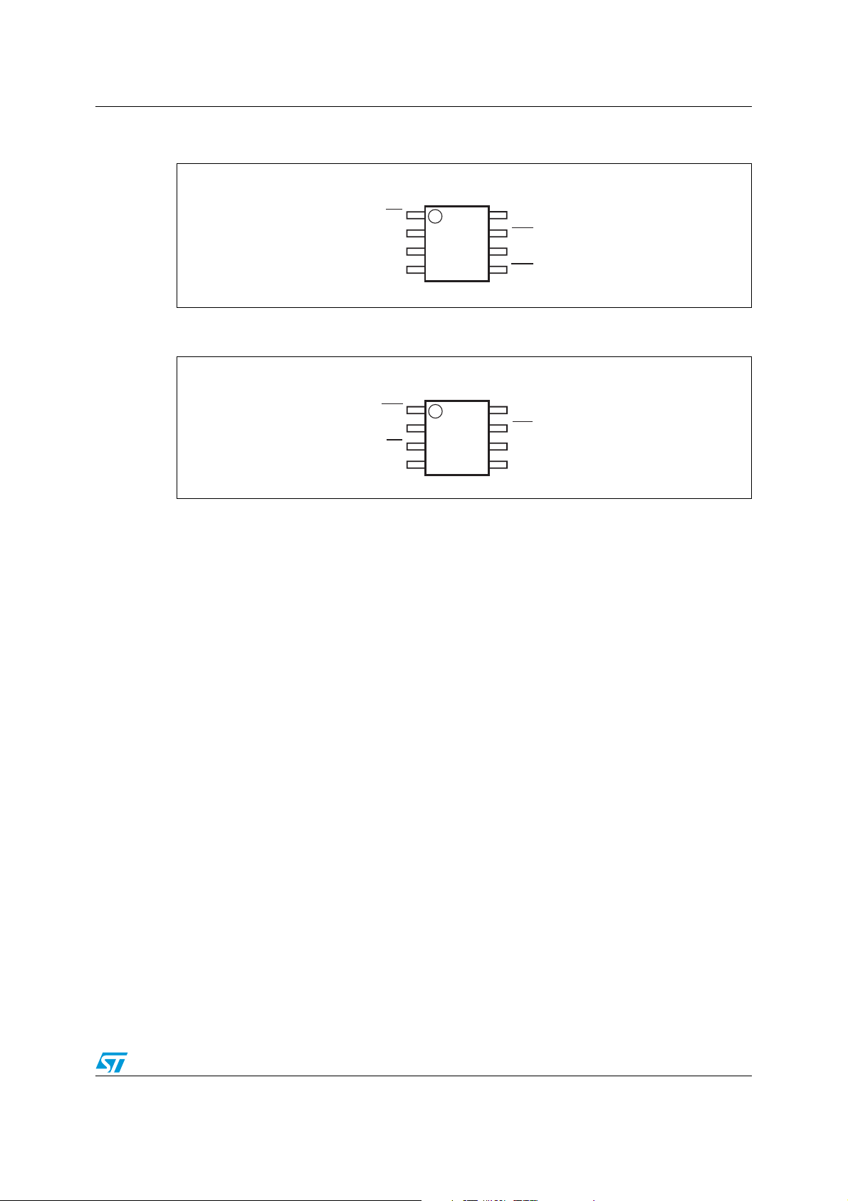
Figure 5. STM707/708 SO8 connections
SO8
MR
V
CC
V
SS
PFI
1
2
3
4
RST
8
RST
7
NC
6
PFO
5
AI08828a
Figure 6. STM707/708 TSSOP8 connections
TSSOP8
RST
RST
MR
V
CC
1
2
3
4
NC
8
PFO
7
PFI
6
V
5
SS
AI09115
Doc ID 10520 Rev 9 7/33

Pin descriptions STM705, STM706, STM707, STM708, STM813L
2 Pin descriptions
2.1 MR
A logic low on MR asserts the reset output. Reset remains asserted as long as MR is low
and for t
driven from a TTL or CMOS logic line, or shorted to ground with a switch. Leave open if
unused.
2.2 WDI
If WDI remains high or low for 1.6 s, the internal watchdog timer runs out and reset
(or WDO
WDI sees a rising or falling edge.
The watchdog function can be disabled by allowing the WDI pin to float.
2.3 WDO
after MR returns high. This active-low input has an internal pull-up. It can be
rec
) is triggered. The internal watchdog timer clears while reset is asserted or when
It goes low when a transition does not occur on WDI within 1.6 s, and remains low until
a transition occurs on WDI (indicating the watchdog interrupt has been serviced). WDO
goes low when V
goes high as soon as V
Note: For those devices with a WDO
is connected to MR
falls below the reset threshold; however, unlike the reset output, WDO
CC
exceeds the reset threshold. Output type is push-pull.
CC
.
2.4 RST
Pulses low when triggered, and stays low whenever VCC is below the reset threshold or
when MR
threshold, or MR
is a logic low. It remains low for t
goes from low to high.
2.5 RST
Goes high with triggered, and stays high whenever VCC is above the reset threshold or
when MR
or MR
is a logic high. It stays high for t
goes from high to low.
2.6 PFI
also
output, a watchdog timeout will not trigger reset unless WDO
after either VCC rises above the reset
rec
after either VCC falls below the reset threshold,
rec
When PFI is less than V
ground if unused.
8/33 Doc ID 10520 Rev 9
, PFO goes low; otherwise, PFO remains high. Connect to
PFI
STM705, STM706, STM707, STM708, STM813L Pin descriptions
2.7 PFO
When PFI is less than V
, PFO goes low; otherwise, PFO remains high. Leave open if
PFI
unused. Output type is push-pull.
Table 3. Pin description
STM813L
— 7 7 RST
— 6 — NC No connect
Pin
STM707
STM708
STM705
STM706
1 1 1 MR
Name Function
Push-button reset input
6 — 6 WDI Watchdog input
8 — 8 WDO Watchdog output (push-pull)
Active-low reset output
7 8 — RST Active-high reset output
2 2 2 VCC Supply voltage
4 4 4 PFI Power-fail input
5 5 5 PFO Power-fail output (push-pull)
3 3 3 V
Ground
SS
Figure 7. Block diagram (STM705/706/813L)
WDI
V
CC
MR
PFI
1. For STM813L only.
V
CC
WDI
transitional
detector
V
RST
V
PFI
WATCHDOG
TIMER
COMPARE
COMPARE
t
rec
generator
WDO
RST (RST)
PFO
(1)
AI08829
Doc ID 10520 Rev 9 9/33
Pin descriptions STM705, STM706, STM707, STM708, STM813L
Figure 8. Block diagram (STM707/708)
V
CC
MR
V
RST
V
CC
COMPARE
t
rec
generator
RST
RST
PFI
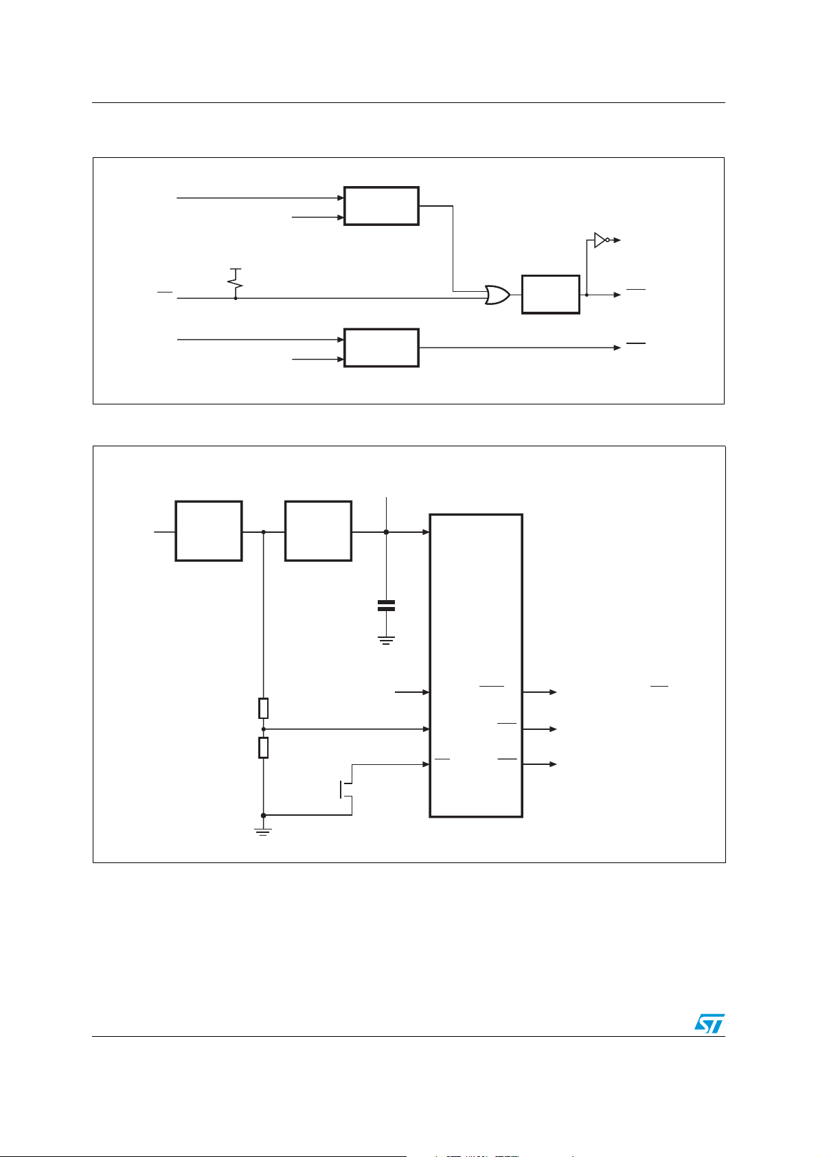
Figure 9. Hardware hookup
Unregulated
voltage
R1
R2
V
CC
COMPARE
0.1 mF
Push-button
V
PFI
Regulator
V
IN
From microprocessor
5 V
V
CC
STM705
STM706
STM707
STM708
STM813L
(1)
WDI
PFI
MR
(1)
WDO
PFO
RST To microprocessor reset
To microprocessor IRQ
To microprocessor NMI
PFO
AI08830
1. For STM705/706/813L.
10/33 Doc ID 10520 Rev 9
AI08831a
 Loading...