

Page 1
Single-chip hardware accelerated encryption engine for
computer and peripherals applications
Features
■ World class encryption engine
– HardCache™ Crypto module
– FIPS 140-2 security level 3
– NIST Certificate #1599
■ Symmetric algorithms (NIST FIPS approved)
– AES Rijndael block cipher: Key length
128/192/256 bits, ECB/CBC/CBC-FVE
modes, NIST Certificate #1068
– Triple DES: Key length 112/168 bits,
ECB/CBC modes, NIST Certificate #798
– SHA-256, SHA-384 and SHA-512 with
associated HMAC: NIST SHS Certificate
#1015, NIST HMAC Certificate #606
■ Asymmetric Algorithms
– ECDSA, 256- and 384-bit elliptic curves
– RSA PKCS#1 v2.1 padding scheme
– 2048 bit operands
■ Algorithm control policy
– Easy algorithm configuration
– Export control
■ PCI Express
■ Advanced 65 nm process technology
■ Windows XP, Windows 2000, Windows Vista,
Windows 7
ECOPACK® ROHS compliant
■
®
x1 interface
(a)
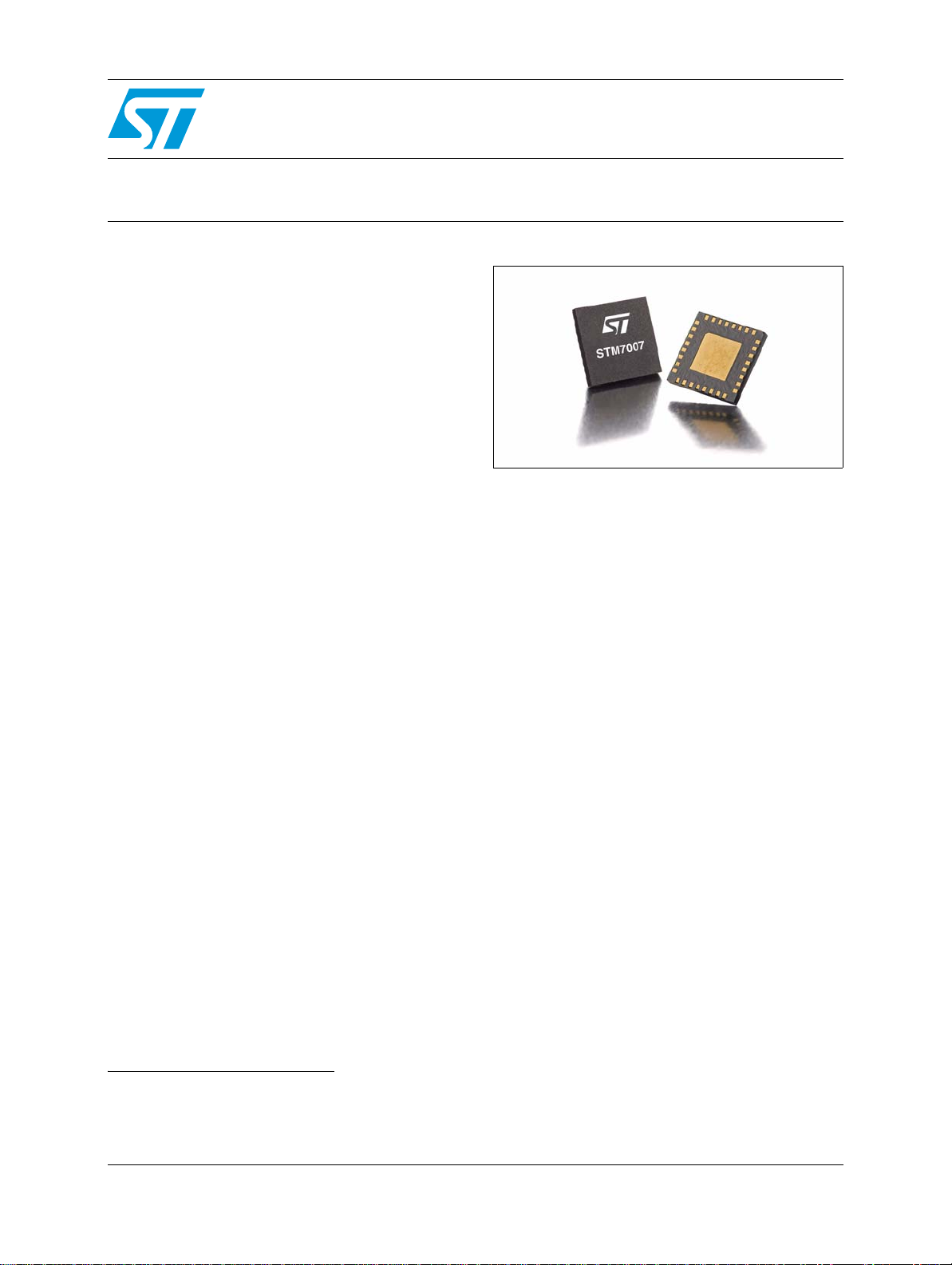
STM7007
Data brief
■ Best in class performance / power ratio
■ Secure key management protected inside a
tamper resistant cryptographic boundary
■ Resists attacks that use software and/or
instrumentation monitors
■ Enables secure remote administration
■ Shielded locations and protected operations
Applications
■ Desktop PC clients
■ Laptop and mobile PC
■ Server and workstation
■ Entire volume encryption
■ Data loss protection
■ Cryptographic service provider
■ Secure messaging
System benefits
Description
■ Off-loads intensive cryptographic calculations
(asymmetric and symmetric) from the system
CPU
■ Out performs SW based solutions and 3 GHz
processors
■ Full duplex DMA operation
a. Windows is a trademark of Microsoft Corporation.
October 2011 Doc ID 022239 Rev 1 1/27
For further information contact your local STMicroelectronics sales office.
The STM7007 is a PCI Express encryption
engine built on the STMicroelectronics’
HardCache™ cryptographic channel controller
(a
high performance core computing block, with
FIPS 140-2 security level 3 certification).
The
STM7007 provides hardware acceleration for
commonly used algorithms, including AES, 3DES,
SHA, HMAC, RSA, and ECC.
www.st.com
1
Page 2

Contents STM7007
Contents
1 Device pinout and package . . . . . . . . . . . . . . . . . . . . . . . . . . . . . . . . . . . 3
1.1 Device pins . . . . . . . . . . . . . . . . . . . . . . . . . . . . . . . . . . . . . . . . . . . . . . . . . 4
1.2 Device package . . . . . . . . . . . . . . . . . . . . . . . . . . . . . . . . . . . . . . . . . . . . . 7
1.2.1 Dimensions . . . . . . . . . . . . . . . . . . . . . . . . . . . . . . . . . . . . . . . . . . . . . . . 8
1.2.2 Recommended footprint . . . . . . . . . . . . . . . . . . . . . . . . . . . . . . . . . . . . . 9
1.2.3 Markings . . . . . . . . . . . . . . . . . . . . . . . . . . . . . . . . . . . . . . . . . . . . . . . . 10
1.2.4 Recommended land pad layout and solder reflow profile . . . . . . . . . . . 11
1.2.5 Rework guidelines . . . . . . . . . . . . . . . . . . . . . . . . . . . . . . . . . . . . . . . . . 13
2 Electrical characteristics . . . . . . . . . . . . . . . . . . . . . . . . . . . . . . . . . . . . 14
2.1 Recommended operating conditions . . . . . . . . . . . . . . . . . . . . . . . . . . . . 14
2.2 Absolute maximum ratings . . . . . . . . . . . . . . . . . . . . . . . . . . . . . . . . . . . . 15
2.3 Environment maximum ratings . . . . . . . . . . . . . . . . . . . . . . . . . . . . . . . . . 15
2.4 Power dissipation . . . . . . . . . . . . . . . . . . . . . . . . . . . . . . . . . . . . . . . . . . . 15
2.5 DC electrical specifications . . . . . . . . . . . . . . . . . . . . . . . . . . . . . . . . . . . 16
2.5.1 PCI, miscellaneous 3.3V interfaces . . . . . . . . . . . . . . . . . . . . . . . . . . . . 16
2.5.2 PHY 1.2V and 2.5V interfaces . . . . . . . . . . . . . . . . . . . . . . . . . . . . . . . . 16
2.6 AC electrical specification . . . . . . . . . . . . . . . . . . . . . . . . . . . . . . . . . . . . 17
2.7 Differential interface electrical characteristics . . . . . . . . . . . . . . . . . . . . . 17
2.7.1 PCIe test circuit . . . . . . . . . . . . . . . . . . . . . . . . . . . . . . . . . . . . . . . . . . . 18
3 PCB layout guidelines . . . . . . . . . . . . . . . . . . . . . . . . . . . . . . . . . . . . . . 19
3.1 PCB Routing of RX/TX differential signals . . . . . . . . . . . . . . . . . . . . . . . . 20
3.1.1 Example: PCB impedance calculation . . . . . . . . . . . . . . . . . . . . . . . . . . 21
3.2 PCB power and ground decoupling guidelines . . . . . . . . . . . . . . . . . . . . 22
3.3 Power sequencing . . . . . . . . . . . . . . . . . . . . . . . . . . . . . . . . . . . . . . . . . . 23
4 Ordering information . . . . . . . . . . . . . . . . . . . . . . . . . . . . . . . . . . . . . . . 25
5 Revision history . . . . . . . . . . . . . . . . . . . . . . . . . . . . . . . . . . . . . . . . . . . 26
2/27 Doc ID 022239 Rev 1
Page 3
STM7007 Device pinout and package
1
1 Device pinout and package
Device pinout, top view . . . . . . . . . . . . . . . . . . . . . . . . . . . . . . . . . . . . . . . . . . . . . . . . . . . . . . . 3
Device pins . . . . . . . . . . . . . . . . . . . . . . . . . . . . . . . . . . . . . . . . . . . . . . . . . . . . . . . . . . . . . . . . 4
Signal types . . . . . . . . . . . . . . . . . . . . . . . . . . . . . . . . . . . . . . . . . . . . . . . . . . . . . . . . . . . . 4
Signal groups . . . . . . . . . . . . . . . . . . . . . . . . . . . . . . . . . . . . . . . . . . . . . . . . . . . . . . . . . . . 4
STM7007 pins . . . . . . . . . . . . . . . . . . . . . . . . . . . . . . . . . . . . . . . . . . . . . . . . . . . . . . . . . . . 4
Device package . . . . . . . . . . . . . . . . . . . . . . . . . . . . . . . . . . . . . . . . . . . . . . . . . . . . . . . . . . . . . 7
Figure 1. Device pinout, top view
PETn
PETp
VDD1V2
rsvd
rsvd
rsvd
PERST#
rsvd
10
11
12
13
14
15
16
VDDR1V2
PERn
7
PERp
6
GND
5
rsvd
8
9
STM7007
32-Pin
LGA 5x5
18
17
VDD3V3
rsvd
19
rsvd
20
rsvd
VDDT1V2
4
21
VDD2V5
VDDPLL1V2
3
22
rsvd
REFCLKn
2
23
rsvd
REFCLKp
24
CLKREQ#
32
31
30
29
28
27
26
25
REFRES
GND_PLL
VDDPLL2V5
VDD1V2
rsvd
rsvd
rsvd
PGOOD
Doc ID 022239 Rev 1 3/27
Page 4
Device pinout and package STM7007
1.1 Device pins
● Ta b le 1 lists the abbreviations used for the signal type names in Tabl e 3 .
Note that abbreviations may be combined, as with APWR (Analog power supply).
● Ta b le 2 lists device signals and how they are grouped, color coding each group.
● Ta b le 3 lists device pins, and uses the same color coding as Tab le 2 to indicate pin
grouping.
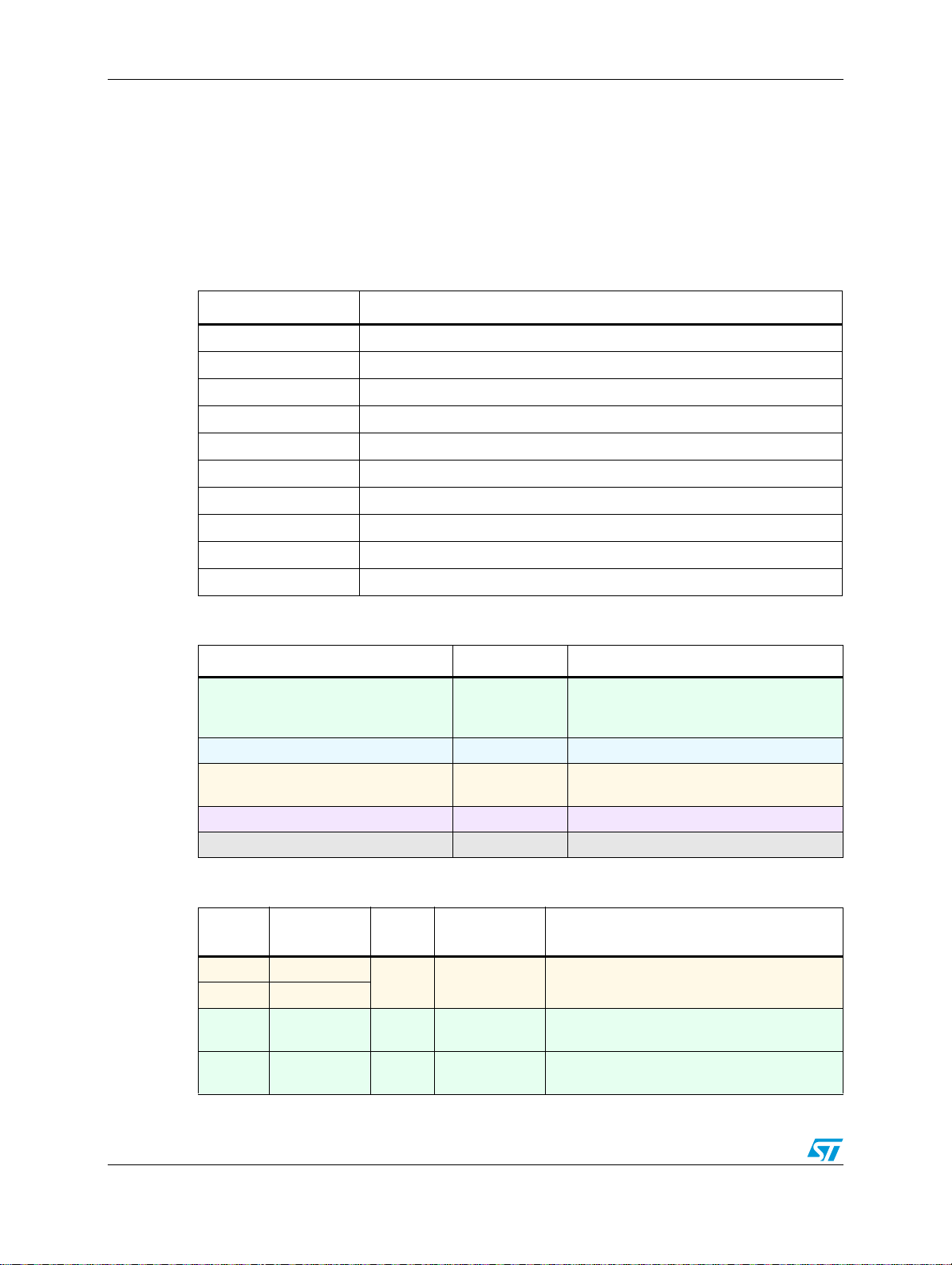
Table 1. Signal types
Abbreviation Description
AAnalog
DI Digital input
DO Digital output
GND Ground
I Input
LVDSI Low voltage differential input
LVDSO Low voltage differential output
NC No connection
O Output
PWR Power supply
Table 2. Signal groups
Signal Group Count (32-pin LGA 5x5 package)
VDD1V2, VDD2V5, VDD3V3,
VDD1V2, VDDPLL1V2, VDDPLL2V5,
Power (VDD) 8
VDDR1V2, VDDT1V2
VSS_PLL, VSS Ground (VSS) 2 (GND pad slug on bottom of device)
PETp, PETn, PERp, PERn, REFCLKp,
REFCLKn, CLKREQ#, PERST#
PCI Express 8
REFRES, PGOOD MISC 3
RSVD Not connected 3
Table 3. STM7007 pins
Pin
number
1 REFCLKp
Pin
name
Signal
(1)
type
External
component
Description
LV DS I — Low voltage differential clock input
2 REFCLKn
3 VDDPLL1V2 APWR
4 VDDT1V2 APWR
Decoupling
capacitor
Decoupling
capacitor
1.2 volt analog power input for the internal
PLL block
1.2 volt analog power input for PCIe transmit
channel
4/27 Doc ID 022239 Rev 1
Page 5
STM7007 Device pinout and package
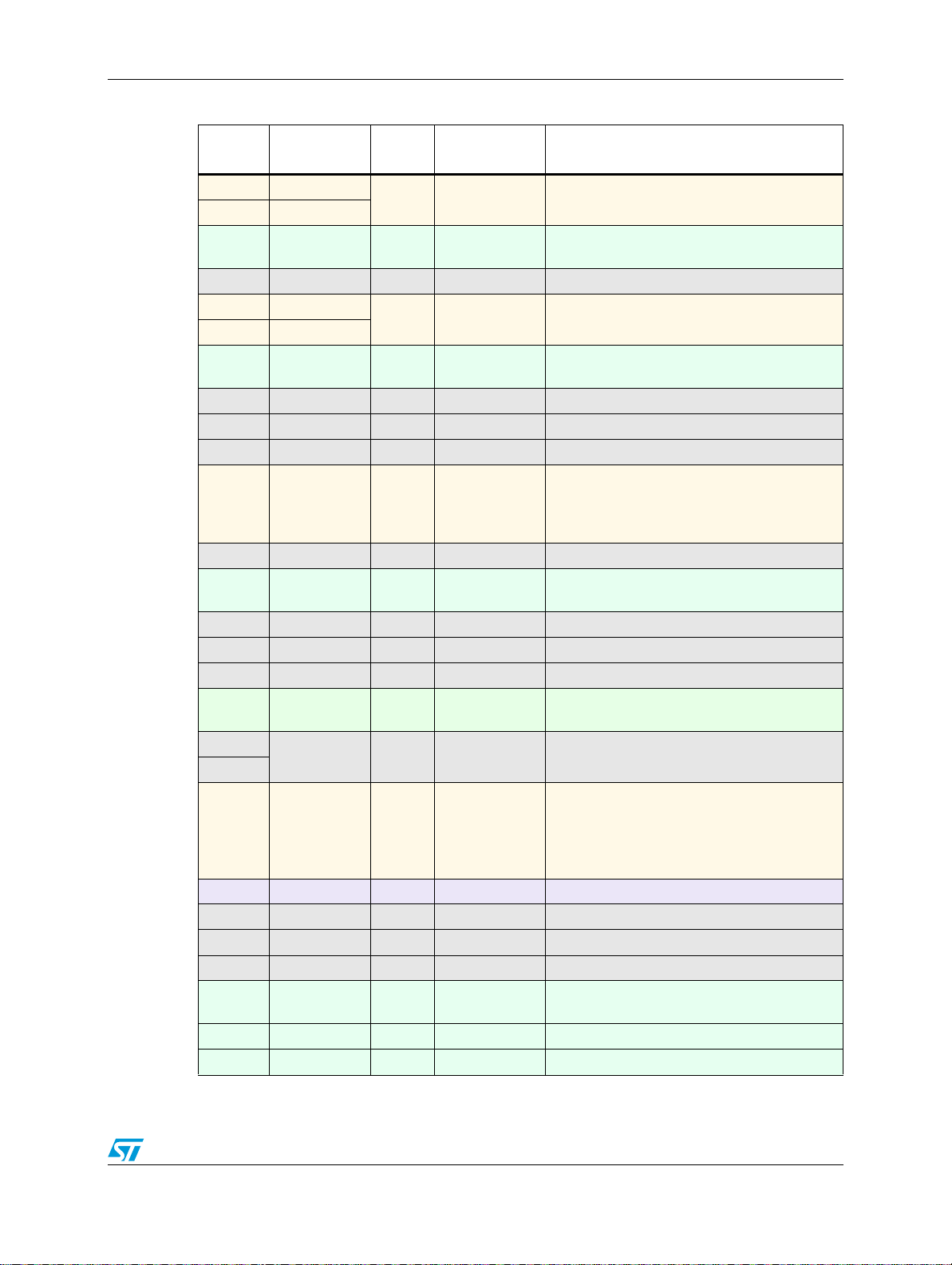
Table 3. STM7007 pins (continued)
Pin
number
Pin
name
Signal
(1)
type
External
component
Description
5 PERn
6 PERp
7 VDDR1V2 APWR
8 RSVD NC Reserved pins, do not connect
9 PETn
10 PETp
11 VDD1V2 PWR
12 RSVD NC — Reserved
13 RSVD NC — Reserved
14 RSVD NC — Reserved
15 PERST# DI —
16 RSVD NC — Reserved
17 VDD3V3 PWR
18 RSVD NC — Reserved
19 RSVD NC — Reserved
20 RSVD NC — Reserved
21 VDD2V5 PWR
22
RSVD NC — Reserved pins, do not connect
23
24 CLKREQ# DO —
25 PGOOD DI — Power on reset, used to reset the core.
26 RSVD NC — Reserved
27 RSVD NC — Reserved
28 RSVD NC — Reserved
29 VDD1V2 PWR
30 VDDPLL2V5 PWR —
31 GND_PLL GND — DC return pin for PLL block
LV DS I — Low voltage differential receive pair
Decoupling
capacitor
LV DS O — Low voltage differential transmit pair
Decoupling
capacitor
Decoupling
capacitor
Decoupling
capacitor
Decoupling
capacitor
1.2 volt analog power input for PCIe receive
channel
1.2 volt power supply input for core
Asynchronous device reset input from
system. When asserted, STM7007 resets all
volatile content and executes a reboot after
de-assertion of signal.
3.3 volt power supply input for I/O logic
2.5 volt power supply
Informs the host controller that the reference
clock input is required by the STM7007. It is
an open drain active low output; when 0, the
reference clock is required, otherwise the
reference clock can be off.
1.2 volt power supply input for core
Doc ID 022239 Rev 1 5/27
Page 6
Device pinout and package STM7007
Table 3. STM7007 pins (continued)
Pin
number
32 REFRES AI Resistor
— GND GND - DC return pad
1. For acronym definitions, see Table 1: Signal types on page 4.
Pin
name
Signal
(1)
type
External
component
Description
Reference resistor input for PLL block. This
pin is tied to 1.2V PLL using a 475_1% ohm
resistor
6/27 Doc ID 022239 Rev 1
Page 7

STM7007 Device pinout and package
1.2 Device package
Dimensions . . . . . . . . . . . . . . . . . . . . . . . . . . . . . . . . . . . . . . . . . . . . . . . . . . . . . . . . . . . . . . . . 8
Recommended footprint . . . . . . . . . . . . . . . . . . . . . . . . . . . . . . . . . . . . . . . . . . . . . . . . . . . . . . 9
Markings . . . . . . . . . . . . . . . . . . . . . . . . . . . . . . . . . . . . . . . . . . . . . . . . . . . . . . . . . . . . . . . . . 10
This device uses a 32-Lead, 5 x 5 x 0.82 mm land grid array (LGA) package.
Note: 1 This package is not yet defined in JEDEC publications.
2 The exact shape of each corner is optional.
Doc ID 022239 Rev 1 7/27
Page 8
Device pinout and package STM7007
1.2.1 Dimensions
Table 4. Package dimensions (mm)
Reference Minimum Typical Maximum
A 0.74 0.82 0.88
A1 0.00 0.035
A3 0.22
b 0.18 0.25 0.30
D 4.90 5.00 5.10
D1 3.50
D2 2.65 2.70 2.75
E 4.90 5.00 5.10
E1 3.50
E2 2.65 2.70 2.75
e0.50
L0.35 0.45
L1 0.075
ddd 0.100
8/27 Doc ID 022239 Rev 1
Page 9
STM7007 Device pinout and package
GND VIA (8)
PCB_Metal: 250 x 325 µm
(1 to 1 ratio to package pad)
PCB_Solder Mask Opening: 300 x 375 µm
GND Pad
PCB Metal: 3600 x 3600 µm
ePad Soldering Area (5)
PCB_Solder Mask Opening: 700 µm dia.
Stencil thickness: 4 mils
Land aperture: 250 x 325 µm (1 to 1 ratio)
ePad soldering aperture: 750 u dia. (slight increase)
Thicker stencil option
Stencil thickness: 5 mils
Land aperture: 275 x 357 µm (10% increase)
ePad soldering aperture: 800 µm dia.
For a thicker stencil, slightly increase the aperture size
for robust solder paste release
(increase area ratio:
area of pad / area of aperture wall).
1.2.2 Recommended footprint
Figure 2. PCB layout recommendation
Figure 3. Stencil layout recommendation
Doc ID 022239 Rev 1 9/27
Page 10
Device pinout and package STM7007
Assembly date (y/ww)
ST logo
2nd level interconnect (e2)
(an ECOPACK
®
parameter)
ECOPACK
®
grade
Metal revision #
(n of N.n)
Assembly sub lot
Diffusion plant
Device base number
Country of origin
Assembly plant
Back-end sequence
Orientation dot
n
7007N
Full-layer revision #
(N of N.n)
PCI GEN1 or GEN2
(1 or 2)
1.2.3 Markings
Device base number: 7007 (four digits)
Device revision number: N.n
N = Full-layer revision number (one digit)
n = Metal revision number (one digit)
Figure 4. Device markings (package face: top)
10/27 Doc ID 022239 Rev 1
In order to meet environmental requirements, ST offers these devices in different grades of
ECOPACK
specifications, grade definitions and product status are available at:
ECOPACK® is an ST trademark.
®
packages, depending on their level of environmental compliance. ECOPACK®
www.st.com.
Page 11

STM7007 Device pinout and package
1.2.4 Recommended land pad layout and solder reflow profile
Pay special attention to the traces connecting to the metal pads on the board. Trace
cracking can occur during normal handling of the board. This trace cracking usually occurs
at the edge of the solder mask opening, around the metal pad.
To avoid this mode of failure, make the trace under the solder mask edge wider than the rest
of the trace, as shown in
connection, the wider part of the trace might need to be as wide as 50 to 75% of the metal
pad width.
Figure 5. Wider trace connection to avoid cracking
Figure 5. Depending on the reliability requirements of the
Doc ID 022239 Rev 1 11/27
Page 12

Device pinout and package STM7007
Solder flow profile
Reflow profile and peak temperature have a strong influence on void formation. Follow the
profile recommendation of the paste suppliers, because this is specific to the requirements
of flux formation. The following two profiles can serve as reference for fine tuning the final
profile that works for your application.
Figure 6. SnPb solder flow profile
Figure 7. Pb-free solder flow profile
12/27 Doc ID 022239 Rev 1
Page 13

STM7007 Device pinout and package
1.2.5 Rework guidelines
Because solder joints are not fully exposed with QFN packages, any touch-up is limited. For
defects underneath the package, the whole package must be removed. Because reflow of
adjacent parts is not desirable during rework, the proximity may complicate the rework
process. Because of the product-dependent complexities, the following provides only a
guideline and a starting point for the development of a successful rework process for this
package.
The rework process comprises the following steps:
1. Component removal
The first step in removal of the component is the reflow of solder joints attaching the
component to the PCB board. Ideally the reflow profile for part removal and attachment
should be the same, but this is not always possible.
– Heat the board from the top side of the component.
– Use a special nozzle to direct the heating in the component area.
– Minimize the heating of adjacent components.
– Start with an air velocity of 15 to 20 liters per minute.
– Avoid excess heating and pad liftoff.
2. Site redress
After removing the component, clean the site properly.
– Use de-soldering braid to remove excess solder.
– Once the residual solder is removed, clean the lands with solvent. The solvent is
usually specific to the type of paste used in the original assembly.
3. Solder paste printing
To achieve a uniform and precise deposition, use a miniature stencil specific to the
component.
Avoid tinning the lands, because the amount of solder applied to the lands cannot be
controlled.
4. Component placement and attachment
Although this type of package does display self-centering abilities, use care in its
placement.
Ideally, the reflow profile for part removal and attachment should be the same, but this
is not always possible.
Heat the board from the top side of the component.
Doc ID 022239 Rev 1 13/27
Page 14

Electrical characteristics STM7007
2 Electrical characteristics
Note: The values in this section are preliminary, and subject to change.
Recommended operating conditions . . . . . . . . . . . . . . . . . . . . . . . . . . . . . . . . . . . . . . . . . . . . 14
Absolute maximum ratings . . . . . . . . . . . . . . . . . . . . . . . . . . . . . . . . . . . . . . . . . . . . . . . . . . . 15
Environment maximum ratings . . . . . . . . . . . . . . . . . . . . . . . . . . . . . . . . . . . . . . . . . . . . . . . . 15
Power dissipation . . . . . . . . . . . . . . . . . . . . . . . . . . . . . . . . . . . . . . . . . . . . . . . . . . . . . . . . . . . 15
DC electrical specifications . . . . . . . . . . . . . . . . . . . . . . . . . . . . . . . . . . . . . . . . . . . . . . . . . . . 16
PCI, miscellaneous 3.3V interfaces . . . . . . . . . . . . . . . . . . . . . . . . . . . . . . . . . . . . . . . . . 16
PHY 1.2V and 2.5V interfaces . . . . . . . . . . . . . . . . . . . . . . . . . . . . . . . . . . . . . . . . . . . . . 16
AC electrical specification . . . . . . . . . . . . . . . . . . . . . . . . . . . . . . . . . . . . . . . . . . . . . . . . . . . . 17
Differential interface electrical characteristics . . . . . . . . . . . . . . . . . . . . . . . . . . . . . . . . . . . . . 17
2.1 Recommended operating conditions
Note: Operation beyond recommended conditions is neither recommended nor guaranteed.
Table 5. Recommended operating conditions
Parameter Minimum Typical Maximum Units Notes
VDD1V2 1.14 1.2 1.26 V Core voltage
VDD2V5 2.375 2.5 2.625 V Antifuse charge-pump
VDD3V3 3.0 3.3 3.6 V I/O voltage for PCIe interface
VDDT1V2 1.14 1.2 1.26 V Transmit channel VDD
VDDR1V2 1.14 1.2 1.26 V Receive channel VDD
VDDPLL1V2 1.14 1.2 1.26 V PLL Core
VDDPLL2V5 2.375 2.5 2.625 V PLL
Ta 0 - 70 C Ambient temperature
14/27 Doc ID 022239 Rev 1
Page 15

STM7007 Electrical characteristics
2.2 Absolute maximum ratings
Caution: Stresses beyond those listed in Tab l e 6 may cause permanent damage to the device;
because these are stress ratings, functional operation is not implied at these or any other
conditions beyond those indicated in Table 5 on page 14. Exposure to the conditions listed
in Ta b le 6 for extended periods may affect device reliability.
Table 6. Absolute maximum ratings
Parameter Minimum(V) Maximum (V) Notes
VDD1V2 -0.5 1.5 Core voltage
VDD2V5 -0.5 3.0 Antifuse charge-pump
VDD3V3 -0.5 4.0 PCI IO Ring
VDDT1V2 -0.5 1.5 Transmit Channel VDD
VDDR1V2 -0.5 1.5 Receive channel VDD
VDDPLL1V2 -0.5 1.5 PLL core
VDDPLL2V5 -0.5 3.0 PLL
1. These are stress ratings, not functional operation ratings.
(1)
2.3 Environment maximum ratings
Table 7. Environment maximum ratings
Parameter Minimum Maximum Units Notes
ESD HBM — 2000 V Human body model
ESD CDM — 500 V Charged device model
Tstorage -40 150 C Storage temperature
2.4 Power dissipation
Table 8. Power dissipation typical mode
Current (mA)
Symbol/mode
Power rails (V)
3.3 2.5 1.2
L0 - AF programming 2 48 216 385.8
L0 - bulk 2 17 222 315.5
L0 - average 2 17 173.4 257.18
L0 - idle 2 17 168 250.7
L0s 2 17 139 215.9
L1 - CLKREQ# asserted 2 17 126 200.3 Clock power management disabled
L1 - CLKREQ# deasserted 1 3 20 34.8 Clock power management enabled
for
Total
(mW)
Notes
Average power, assuming 10% duty cycle
(0.1 * L0-Bulk + 0.9 * L0-Idle)
Doc ID 022239 Rev 1 15/27
Page 16

Electrical characteristics STM7007
2.5 DC electrical specifications
2.5.1 PCI, miscellaneous 3.3V interfaces
Note: 1 While I/O is in high impedance state
2 Does not include current flowing through termination resistors.
Table 9. 3.3V interface pin DC specifications
Parameter Symbol
Test
condition
Minimum Typical Maximum Units Notes
Input low level VIL -0.3 — 0.8 V
Input high level VIH 2.0 — 0.3 + VDD3V3 V
Output low level VOL 8 mA — — 0.4 V
Output high level VOH 8 mA VDD3V3 - 0.4 — — V
Input leakage
current
IIL 0<VIN<VDD3V3 < 1 (25
o
C) — 2 (125o C) μA1;2
Pin capacitance CPin 30 — pF
2.5.2 PHY 1.2V and 2.5V interfaces
Table 10. 1.2 and 2.5 PHY interface pin dc specifications
1.2V supply voltage range VDD1V2 1.14 1.2 1.26 V
Supply ripple (1 MHz to 3 GHz) VDD1V2ripple — — 50 mV (pk-pk)
2/5V supply voltage range VDD2V5 2.375 2.5 2.625 V
Supply ripple (1 GHz to 3 GHz) VDD2V5ripple — — 50 mV (pk-pk)
Maximum reference clock input jitter.
RJ component bounded at +/- 7 sigma
Parameter Symbol Minimum Typical Maximum Units
TJrefclk — — 30 ps (pk-pk)
16/27 Doc ID 022239 Rev 1
Page 17

STM7007 Electrical characteristics
2.6 AC electrical specification
Table 11. PCI Express clock input
Parameter Description Minimum Typical Maximum Units
PCIe pin RefClkp, RefClkn
Fref
The clock must be compliant
with the LVDS input driver level.
99.97 100 100.03 MHz
2.7 Differential interface electrical characteristics
Table 12. PCIe Interface driver and receiver characteristics
Description Symbol Minimum Maximum Units
Baud rate BR 2.5 Gbps
Unit interval UI 399.88 400.12 ps
Baud rate tolerance BRtol -300 300 ppm
Driver parameters
Differential peak to peak output voltage VTXpp 800 1200 mV
Minimum Tx eye width TTxeye 0.750 UI
Differential return loss TRLdiff 10 dB
Common mode return loss TRLcomm 6 dB
DC differential TX impedance ZTXdiff 85 115
Ω
Receiver parameters
Differential peak to peak voltage VRXpp 0.175 1.2 V
Minimum Rx eye width TRxeye 0.4 UI
Differential return loss TRLdiff 10 dB
Common mode return loss RRLcomm 6 dB
DC differential RX impedance ZRXdiff 85 115
DC single-ended input impedance ZRXDC 40 60
Ω
Ω
Doc ID 022239 Rev 1 17/27
Page 18

Electrical characteristics STM7007
2.7.1 PCIe test circuit
When measuring transmitter output parameters, C_TX is an optional portion of the
test/measurement load.
When used, the value of C_TX must be in the range of 75 to 200 nF. C_TX must not be used
when the test/measurement load is placed in the receiver package reference plane.
Figure 8. PCIe test circuit
18/27 Doc ID 022239 Rev 1
Page 19

STM7007 PCB layout guidelines
3 PCB layout guidelines
PCB Routing of RX/TX differential signals . . . . . . . . . . . . . . . . . . . . . . . . . . . . . . . . . . . . . . . 20
PCB power and ground decoupling guidelines . . . . . . . . . . . . . . . . . . . . . . . . . . . . . . . . . . . . 22
Power sequencing . . . . . . . . . . . . . . . . . . . . . . . . . . . . . . . . . . . . . . . . . . . . . . . . . . . . . . . . . . 23
The STM7007 uses high speed, low voltage differential signal pairs for the PCIe interface.
For a successful board design, follow the placement and layout guidelines in this chapter for
critical signals. Additional application notes may be provided for more detailed requirements.
The STM7007 is designed for optimized wiring for both a motherboard or PCI Express
mini-card form factor. Pin locations of the critical high speed LVDS signals are designed to
support a seamless flow from the STM7007 to the upstream host controller.
See also, Figure 1: Device pinout, top view.
Doc ID 022239 Rev 1 19/27
Page 20

PCB layout guidelines STM7007
3.1 PCB Routing of RX/TX differential signals
Ensure that the board design meets the following criteria:
● To avoid skew, make signal pair lengths equal from the ball to the connector:
TXP length = TXN length, and RXP length = RXN length
Lengths may differ if required to compensate for length mismatch due to poor package
substrate routing.
● Route signal pairs in parallel
● Ensure a 100Ω differential impedance trace:
– Route signals on an external layer with a full or partial ground plane layer as the
next internal adjacent layer. A partial ground plane must cover and exceed the
area below the TX and RX signal routing.
– Between the package pin and the PCI-Express connectors, ensure equal signal
trace interspace distance on each pair along the entire trace length.
● To avoid crosstalk:
– Separate TX and RX pairs a minimum of 5 mm, with no other signals interleaved.
– If several ports are routed, do not route the TX and RX traces of each port one
above the other on different layers.
● Do not use:
– Right angles or 45-degree trace angles; curved traces are preferred
–PCB vias
● Make all traces:
– As direct and straight as possible
– As short as possible. Signal line attenuation may be compensated for by selecting
a higher buffer swing, but if the largest swing is specified for the application, there
is no capacity for swing compensation.
● If components (such as AC coupling capacitors) are required on the high speed signal
traces, choose the smallest SMD packages and place them close to connectors.
● PCB trace crossing: if two differential traces from different ports must cross, cross the
traces at 90
º (perpendicular) to each other.
20/27 Doc ID 022239 Rev 1
Page 21

STM7007 PCB layout guidelines
3.1.1 Example: PCB impedance calculation
The PCB manufacturer should provide the board designer with all relevant parameters for
calculating trace impedance:
● trace thickness
● trace width
● PCB material, giving E
●
distance between layer 1 and internal layer 2
● coating thickness
Example calculation
Differential pair routed on top layer (1)
Trace width: 7 mils
Inter-space trace distance: 7 mils
r
Ground plane on internal layer 2, giving 5.9 mils dielectric height (E
= 3.9)
r
Trace thickness: 40 μm = 1.6 mils.
The calculator shown in Figure 9 gives a theoretical Z
= 101.6Ω.
diff
The PCB manufacturer double-checked with its tools and a more complex calculator, taking
into account the cross-section form of the top layer trace and the coating used. The PCB
manufacturer’s calculation gives a theoretical Z
= 100.2Ω.
diff
Figure 9. UltraZ calculation for differential pair impedance
Doc ID 022239 Rev 1 21/27
Page 22

PCB layout guidelines STM7007
3.3V I/O Rail
PCI Express Mini Card connector
For mobile form-factor: support for clock power management (CLKREQ#)
PCI Express connector
For ATX/mini-ATX form-factor: no support for clock power management (CLKREQ#)
PCI Express connector
REG
REG
1.2V RX
2.5V Antifuse
2.5V PLL
1.2V Core
1.2V PLL
1.2V TX
STM7007
3.2 PCB power and ground decoupling guidelines
Figure 10. Power map
All grounds: Connect directly to the PCB common ground plane
Power pins VDDR1V2 and VDDT1V2:
● Directly connect to the board’s 1.2V common supply dedicated to the PHY
● Decouple locally using:
– Murata Ferrite BLM15AG121 or equivalent
–1.0 μF ceramic capacitor
–0.1 μF RF capacitor (low series access resistor)
–0.01 μF RF capacitor (low series access resistor)
Power pin VDDPLL1V2:
● Directly connect to the board’s 1.2V common supply dedicated to the PHY
● Filter locally using:
–1Ω resistor
–10 μF ceramic capacitor
–0.1 μF RF capacitor (low series access resistor)
–0.01 μF RF capacitor (low series access resistor)
Power pin VDD2V5:
● Directly connect to the board‘s 2.5V common supply dedicated to the PHY
● Filter locally using:
–1Ω resistor
–1.0 μF ceramic capacitor
– 100 pF RF capacitor (low series access resistor)
– 10 nF RF capacitor (low series access resistor)
22/27 Doc ID 022239 Rev 1
Page 23

STM7007 PCB layout guidelines
Power pin VDDPLL2V5:
● Directly connect to the board’s 2.5V common supply dedicated to the PHY
● Filter locally using:
–30Ω resistor (±5% maximum tolerance)
–0.1 μF RF capacitor (low series access resistor)
–0.01 μF RF capacitor (low series access resistor)
3.3 Power sequencing
The STM7007 requires proper supply voltage and PGOOD (power good) sequencing for the
internal power-on-self-test and the antifuse blocks.
requirements.
The primary requirement for this device is PGOOD timing; PGOOD must provide a valid
status of the supply voltages during power sequencing.
The PGOOD signal:
● remains inactive until all voltages are within their required tolerance bands during
power up
● goes inactive before the supply voltages exit their required tolerance bands during
power down
The first indication that power-down sequencing is occurring, is the dropping of the 3v3
input supply voltage.
Figure 11 shows the timing and level
The PGOOD input pin and the PERST# input pin are logically combined internally to ensure
the proper reset state of the device during sequencing.
The 2v5 and 1v2 regulators must be sourced by the 3v3 supply such that the recommended
order of supply sequencing at power up is 1v2 first and then 2v5, and at power down 2v5
drops first, and then 1v2.
Because of an internal ESD protection diode, it is expected that when the 1v2 is applied to
the VDDPLL1V2 pin, the VDDPLL2V5 pin will source voltage at a level equal to the 1v2
voltage minus the forward voltage drop of a diode. To limit the diode current, and to provide
lowpass filtering of the PLL 2V5 power source, place a 30
Ω, 5% resistor between the
VDOPLL2V5 pin and the 2V5 source. Position the bypass capacitors close to the
VDDPLL2V5 pin (pad).
Doc ID 022239 Rev 1 23/27
Page 24

PCB layout guidelines STM7007
3v3 Input
1v2
2v5
PGOOD
Power Up
Power Down
950 mV Min.
100 mV
Max.
2.25 V Min.
10 us Min.
800 mV
Max.
2.0 V Min.
3.6 V Max.
3.60 V Max.
3.00 V Min.
2.25 V Min.
2.75 V Max.
800 mV
Max.
10 us Min.
100 mV
Max.
2.25 V Min.
3.00 V Min.
PERST#
(alternate)
1.32 V Max.
1.08 V Min.
10 us Min.
2.0 V Min.
3.6 V Max.
800 mV
Max.
3.00 V Min.
0.0 us Typ.
10 us Min.
800 mV
Max.
1.08 V Min.
Figure 11. Power up / down timing requirements
24/27 Doc ID 022239 Rev 1
Page 25

STM7007 Ordering information
4 Ordering information
When ordering parts, use the information below and contact your local STMicroelectronics
sales office, field applications engineer, or manufacturer’s representative for further
information.
Table 13. STM7007 ordering information
Order code Package type Note
STM7007 32-Pin LGA 5x5 Commercial RoHS and halogen free package
Doc ID 022239 Rev 1 25/27
Page 26
Revision history STM7007
5 Revision history
Table 14. Document revision history
Date Revision Changes
06-Oct-2011 1 Initial release.
26/27 Doc ID 022239 Rev 1
Page 27

STM7007
Please Read Carefully:
Information in this document is provided solely in connection with ST products. STMicroelectronics NV and its subsidiaries (“ST”) reserve the
right to make changes, corrections, modifications or improvements, to this document, and the products and services described herein at any
time, without notice.
All ST products are sold pursuant to ST’s terms and conditions of sale.
Purchasers are solely responsible for the choice, selection and use of the ST products and services described herein, and ST assumes no
liability whatsoever relating to the choice, selection or use of the ST products and services described herein.
No license, express or implied, by estoppel or otherwise, to any intellectual property rights is granted under this document. If any part of this
document refers to any third party products or services it shall not be deemed a license grant by ST for the use of such third party products
or services, or any intellectual property contained therein or considered as a warranty covering the use in any manner whatsoever of such
third party products or services or any intellectual property contained therein.
UNLESS OTHERWISE SET FORTH IN ST’S TERMS AND CONDITIONS OF SALE ST DISCLAIMS ANY EXPRESS OR IMPLIED
WARRANTY WITH RESPECT TO THE USE AND/OR SALE OF ST PRODUCTS INCLUDING WITHOUT LIMITATION IMPLIED
WARRANTIES OF MERCHANTABILITY, FITNESS FOR A PARTICULAR PURPOSE (AND THEIR EQUIVALENTS UNDER THE LAWS
OF ANY JURISDICTION), OR INFRINGEMENT OF ANY PATENT, COPYRIGHT OR OTHER INTELLECTUAL PROPERTY RIGHT.
UNLESS EXPRESSLY APPROVED IN WRITING BY TWO AUTHORIZED ST REPRESENTATIVES, ST PRODUCTS ARE NOT
RECOMMENDED, AUTHORIZED OR WARRANTED FOR USE IN MILITARY, AIR CRAFT, SPACE, LIFE SAVING, OR LIFE SUSTAINING
APPLICATIONS, NOR IN PRODUCTS OR SYSTEMS WHERE FAILURE OR MALFUNCTION MAY RESULT IN PERSONAL INJURY,
DEATH, OR SEVERE PROPERTY OR ENVIRONMENTAL DAMAGE. ST PRODUCTS WHICH ARE NOT SPECIFIED AS "AUTOMOTIVE
GRADE" MAY ONLY BE USED IN AUTOMOTIVE APPLICATIONS AT USER’S OWN RISK.
Resale of ST products with provisions different from the statements and/or technical features set forth in this document shall immediately void
any warranty granted by ST for the ST product or service described herein and shall not create or extend in any manner whatsoever, any
liability of ST.
ST and the ST logo are trademarks or registered trademarks of ST in various countries.
Information in this document supersedes and replaces all information previously supplied.
The ST logo is a registered trademark of STMicroelectronics. All other names are the property of their respective owners.
© 2011 STMicroelectronics - All rights reserved
STMicroelectronics group of companies
Australia - Belgium - Brazil - Canada - China - Czech Republic - Finland - France - Germany - Hong Kong - India - Israel - Italy - Japan -
Malaysia - Malta - Morocco - Philippines - Singapore - Spain - Sweden - Switzerland - United Kingdom - United States of America
www.st.com
Doc ID 022239 Rev 1 27/27
 Loading...